Fast Flip-Chip Pin-Out Designation Respin for
Package-Board Codesign
Ren-Jie Lee, Student Member, IEEE, and Hung-Ming Chen, Member, IEEE
Abstract—Deep submicrometer effects drive the complication in
designing chips, as well as in package designs and communications between package and board. As a result, the iterative interface design has been a time-consuming process. This paper proposes a novel and efficient approach to designating pin-out, which is a package ball chart describing pin locations for flip-chip BGA package when designing chipsets. The proposed approach can not only automate the assignment of more than 200 input/output (I/O) pins on package, but also precisely evaluate package size which accommodates all pins with almost no void pin positions, as good as the one from manual design. Furthermore, the practical experience and techniques in designing such interface has been accounted for, including signal integrity, power delivery and routability. This efficient pin-out designation and package size estimation by pin-block design and floorplanning provides much faster turn around time, thus enormous improvement in meeting design schedule. Our pin-block design contains two major parts. First, we have pin-block construction to locate signal pins within a block along the specific patterns. Six pin patterns are proposed as templates which are automatically generated according to the user-defined constraints. Second, we have pin-blocks grouping to group all pin-blocks into package boundaries. Two alter-native pin-blocks grouping strategies are provided for various applications such as chipset and field-programmable gate array (FPGA). The results on two real cases show that our methodology is effective in achieving almost the same dimensions in package size, compared with manual design in weeks, while simultane-ously considering critical issues and package size migration in package-board codesign.
Index Terms—Package-board codesign, pin-block
floorplan-ning, pin-out designation.
I. INTRODUCTION
B
ECAUSE of deep submicrometer (DSM) technology, chips now contain more functionality and are being driven to higher performance levels than ever before. Consequently, with more functionality on the chip, designers have to deal with higher input/output (I/O) densities, more signals coming out of a chip and tighter geometries [9]. This leads to the complication in designing package which accommodates chips, as well as the board which accommodates the packages. As a result,Manuscript received May 02, 2007; revised October 26, 2007 and March 14, 2008. First published June 02, 2009; current version published July 22, 2009. This work was supported in part by the National Science Council of Taiwan ROC under Grant NSC 97-2220-E-009-001 and Grant NSC 97-2221-E-009-174-MY3.
The authors are with the Department of Electronics Engineering, National Chiao Tung University, Hsinchu 300, Taiwan (e-mail: rjlee@vda.ee.nctu. edu.tw; hmchen@mail.nctu.edu.tw).
Digital Object Identifier 10.1109/TVLSI.2009.2017795
the ability to design the chip, the package, and surrounding system concurrently becomes a primary advantage, but also a challenge.
Recently chip-package codesign has drawn attention under these circumstances, for example [3], [12]. However package-board codesign, which is definitely not a trivial work, still needs more works. Several works [5], [13], [4], [2] which were related to package and printed circuit board (PCB) physical designs. Reference [5] presented a style for ball grid array (BGA) ball-out, but shielding pins used for preventing pin-to-pin crosstalk were not considered. Moreover, when they try to keep the package cost small, this style will put a restriction on the maximum package size. Thus, there is a limit to the number of BGA balls that can be used for power delivery, and area for power delivery from motherboard to package. Reference [13] proposed an algorithm which assigned and routed the solder bumps of a BGA package to a set of fan-out points in a single layer. This work only created a topological routing, not precise geometry layout, and only the routability issue on PCB is considered.
For pin assignment problem, [4] presented a simulated an-nealing algorithm to find a pin assignment solution which con-sidered the routability issue on BGA package and PCB, but no other DSM effects were considered. Reference [2] suggested a direction of research for topological pin assignment. The two-stages heuristic algorithms, initial pin assignment and assign-ment improveassign-ment, can be closely attuned to a specific router, then enhance the routability of PCB by reducing wiring conges-tion and path crossovers. Since this methodology disregarded the package pin number, it can not be applied to assign the pin-out of flip-chip BGA package which has large number of pins and significant cost issue. All these researches are not suit-able for modern package-board codesign, which is requested to have minimal turn around time and optimized signal perfor-mance as well as package cost.
Fig. 1(a) shows the typical interface design flow for IC-package-PCB codesign. In general, IC designers finish the pin designation based on experience (rule-of-thumb). In order to tradeoff signal performance and package cost, they always take few weeks to modify package size, rework package substrate and PCB layout, then rearrange pin-out. This conven-tional process can not efficiently estimate an accurate package size during designating pins for flip-chip BGA and possibly degrade signal performance due to the weakness on product experience and basic design concept. Furthermore, these costly rework constantly postpone the schedule of chip implemen-tation, thus lengthen the time to market (TTM). Fig. 1(b) illustrates our proposed design flow. To begin with, we will
Fig. 1. (a) Typical flow and (b) proposed approach in interface design plan-ning for IC-package-board codesign. Our approach will significantly shorten the runtime throughout the automation process. It cannot only automate pin-out designation efficiently, but also optimize package size during design stage, thus reduce the time of iteration.
create the rough pin configuration, which includes only four essential parameters. We automatically determine the pin-block order through an intuitive manner and flexibly design an ap-propriate pin pattern by solving ILP problems. After finishing the pin configuration, the designers will obtain the optimized package size and die size by automatically designating pin-out and locating I/O buffers. This paper aims at presenting a novel approach to designating pin-out and replacing heavy-loaded human design by automation process, which accounts for practical experience and techniques.
In this paper, we have formulated feasible constraints for au-tomatically designing pin patterns, which are used to assign the signal pins along the particular constraints and work as tem-plates. And then we proposed six signal-pin patterns for pin-block construction in package design. Signal integrity, power delivery, and routability have been accounted for in those pat-terns. This helps to speed up the process of pin-out designa-tion. Furthermore, we have proposed a near optimal approach to minimizing package size by mathematical (linear) program-ming formulation. The package size migration issues are also considered through a simple estimation. The experimental re-sults show that our solution can achieve almost the same rere-sults as manually designed by experienced designers, with much less time.
The remainder of the paper is organized as follows. Section II discusses the flip-chip BGA package design with PCB and
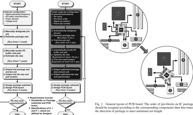
Fig. 2. General layout of PCB board. The order of pin-blocks on IC package should be assigned according to the corresponding components then fine-tuned the direction of package to meet minimum net-length.
DSM effects consideration, while Section III describes our pin-out designation by near optimal planning in package size. Section IV shows the experimental results, followed by the conclusion in Section V. An extended abstract of this paper with less detailed automation processes and without the alter-native strategies for pin-blocks grouping and the considerations of package size migration issues (in Section III) was published by the ASP-DAC 2007 [8].
II. PIN-OUT DESIGNATION BY CONSIDERING
SIGNAL INTEGRITY ANDPOWERDELIVERY IN
PACKAGE-BOARDCODESIGN
When we are designating pin-out, there are several critical constraints and considerations we need to take care of. In this section, we will discuss them comprehensively then introduce the design of pin pattern which can take all the constraints and considerations into account.
A. Constraints and Considerations
1) Locations of PCB Components: Fig. 2 depicts a sketch of
PCB layout. Usually PCB board contains several kinds of com-ponents and connectors which are applied to specific interfaces. The length of signal net from package pin to component or con-nector on PCB is the primary contributor to parasitic inductance. Therefore, package pins will exacerbate simultaneous switching noise (SSN) by increasing the parasitic inductance in the signal nets [7]. The familiar equation shown below describes the basic mechanism of SSN ( ):
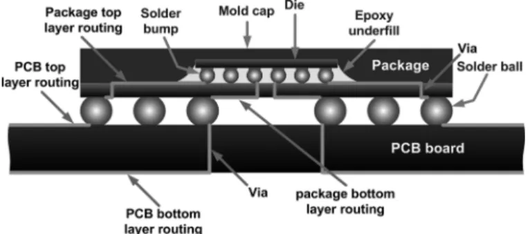
Fig. 3. Simplified cross-section of a flip-chip package which is mounted on PCB board.
where is the number of switching drivers, is the equiv-alent inductance in which current must pass through, and is the current per driver. In order to minimize the physical length of the signal net and thus reduce the total parasitic inductance, package pins should be accommodated in particular regions. As shown in Fig. 2, the minimum net-length can be obtained by as-signing the order of pin-blocks according to the certain location of corresponding components or connectors then fine-tuning the direction of package properly.
2) Routability: Another crucial factor of successful pin
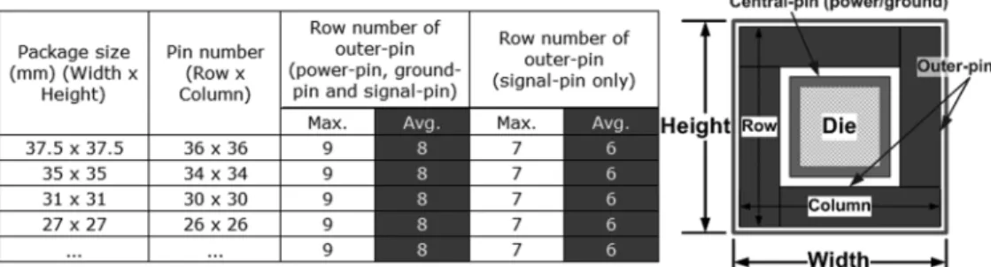
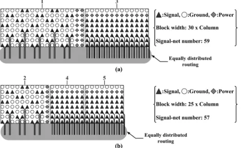
des-ignation is routability. For routing issue, the inflexible package-board routing rules force the row number of signal pins, signal net width and spacing on PCB to be critical constraints. Fig. 3 shows the simplified cross-section of a flip-chip package which is mounted on PCB board. For a general 4-layer PCB board, only the top and bottom layers are allowed to be routed nets; the second and third layers are used for planning power/ground plane. Based on the rules of thumb, package outer pins (solder balls located close to the package edge) connect solder bumps through vias and package top layer routing. These outer pins are then inevitably routed on PCB top layer. On the other hand, package inner pins located around the core of package must con-nect solder bumps by package bottom layer routing and then are routed on PCB bottom layer. Fig. 4 demonstrates the routing pattern on PCB top layer and package bottom layer respectively. For instance, when the diameter of PCB pad is 14 mil (1 mil 25.4 m), pad pitch is 39.37 mil, signal net width and spacing are both 5 mil on a 4-layer PCB board, the space between two pads can only be penetrated by two nets. It means only three rows of signal pins can be fanned out nets on PCB top layer. Because of these routing rules, the excess row number of signal pins will undoubtedly cause routing congestion due to restricted area between pins. Fig. 5 lists the confined row number of signal pins is constant and independent of the package sizes. In our example, the maximum row number of outer pins is nine and that of signal pins is seven (this happens when the nets on PCB bottom layer can be connected to those four rows of signal pins).
3) Signal Integrity: According to the routing pattern, shown
in Fig. 4, we can generalize the rule of thumb in assigning pins. That is, if signal pins are allocated on the same row, their nets can have balanced routing, which means these nets will have matched impedance on PCB and package layout. On the other hand, if signal pins are allocated on the same column, there are only some nets which can have balanced routing. The matched
impedance is an essential requirement for high speed differential systems, because it can eliminate the common mode noise thus improve the signal performance. For signal integrity reason, re-turn path inductance is another main course. The unsuitable placement and number of return path pins, which are power or ground pins, will maximize current return loops and increase return path inductance. This will dramatically degrade signal integrity and exacerbate radiated emissions. Its mechanism is similar to that of SSN and has been shown in (1). In regard to crosstalk noise, one of the major root causes is mutual ca-pacitance [7], mainly because it will inject a current onto the neighbor victim pins. The induced noise ( ) is propor-tional to the mutual capacitance ( ) and the rate in change of voltage on driven pins ( )
(2) Therefore, the optimal pin designation is to place signal pin and power/ground pin proximally close to each other, so that each signal pin can be tightly coupled to a return path pin. This will minimize the effect of the return path inductance. Furthermore, if signal pins surrounded with ground pins, the mutual capac-itance will be decreased and the noise is shielded extremely. In [6], [10], and [11], the effects of shielding, return path and reference plane are considered in package and PCB designs. However, those optimized designs, in terms of signal integrity concern, will create signal-pin blocks which have more power/ ground pins but fewer signal pins within a large block area. The feasible designs of pin pattern are proposed in Section II-B.
B. Pin Pattern Design
In order to automatically and flexibly design an appropriate pin pattern- we formulate the design constraints discussed in last section as feasible ILP problems. Therefore, we can obtain the proper pin patterns after solving the following ILP problems:
for signal pins
for power/ground pins (3)
(4)
(5) (6)
(7) for using power pins
for using ground pins (8)
where ( ), and are the
signal-pin number per pattern, row number and column number of a pattern, respectively.
Equation (4) is the signal pin capacity ( ). It confines the signal pin number within a column for all patterns ( ). As our previous discussion, the average number of this value is six. Equation (5) is the differential signaling constraints ( ).
Fig. 4. (a), (b) Routing pattern on PCB top layer and (c), (d) package bottom layer. Because of the routing rules and restricted area between pins, the confined row number of signal pins is six. The excess row number of signal pins will cause routing congestion during the package substrate and PCB routing phase.
Fig. 5. Restricted row number of signal-pin is constant and independent of package size due to inflexible package-board routing rules (PCB pad = 14 mil, pad pitch = 39.37 mil, net width = 5 mil, net spacing = 5 mil, for four layer PCB board).
The differential signal pins which exist in specific patterns must be strictly assigned at adjacent location in the same row (e.g., , iff ). Equation (6) is the ratio of signal-to-return path pin ( ). The return path pins play an import role in signal integrity considerations, designers must define the es-sential ratio for each pattern according to its applications. Equa-tion (7) is the ratio of signal-to-shielding pin ( ). For the purpose of isolating crosstalk noise, designers can set higher ratio of signal-to-shielding pin to assign ground pin in the neigh-boring location of signal pin. Otherwise, the ratio can be disre-garded for low cost consideration. Obviously, these two ratios and will significantly trade off the performance and cost when we are designing pin patterns. Equation (8) is the type of return path pin ( ). Once the type of return path pin match that of PCB reference plane, the return path will induce the lower parasitic inductance [7]. Hence, this constraint should be defined along the type of reference plane (power/ground) on PCB.
For two layers PCB routing, Table I proposes six sets of con-straints for generating six options of signal-pin patterns ( and represent the fore-half and back-half of patterns). There exists tradeoff between signal performance and package
TABLE I
CONSTRAINTS OFPROPOSEDPINPATTERNS
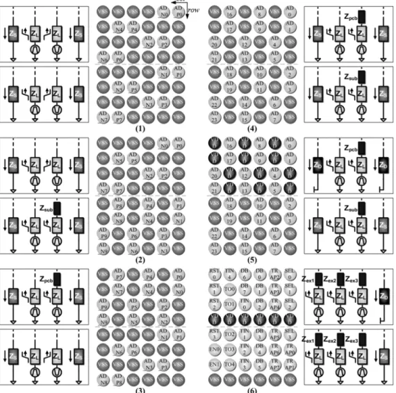
cost. Fig. 6 illustrates these proposed pin patterns and their sim-plified impedance models. The impedance of each net is com-posed of three components: serial resistor, serial inductor and shunt capacitor ( ). The first signal-pin pattern depicts that each pair of differential signal has been sur-rounded by ground pins. These ground pins can be performed as adjacent return path pins to minimize total inductance and
Fig. 6. Six pin patterns proposed in this paper. There exists tradeoff between routability and signal integrity concerns. The first pin pattern has better signal integrity, while the sixth one has the most efficient pin designation. In those patterns, AD_P0/AD_N0 is for differential signal (high speed), AD is for single-ended signal (high speed), and SEL or TRAP in sixth pattern are for single-ended signal (low speed or long-pause signal).
as shielding pins to isolate pin-to-pin crosstalk noise. More-over, the primary concern of differential system is on impen-dence-matching of nets. The first pattern has an exclusive ad-vantage of nets balancing on PCB as well as package substrate layout, shown in Fig. 4(a) and (c). Thus, it is optimal for dif-ferential signals from the performance perspective, and can be modeled by two nets with matched impedance , as shown in Fig. 6. The only disadvantage of this pattern is poor pin desig-nation efficiency.
In most cases, if the return current of a signal pin flows on ground planes, it should be coupled to ground pins to result in minimum return path, or vice versa. Whether a signal is cou-pled to just one power pin or just one ground pin, this case will emerge from the particular signal type and its configuration. Therefore, the fourth and fifth signal-pin patterns are proposed to provide two options for specific bus. The fifth pattern has better power delivery characteristic than the fourth one because of locating power pins. These two patterns arrange pins more efficiently than first pattern, but they both have worse signal integrity on PCB top-layer-routing and package bottom-layer-routing due to poor impedance-matching, shown
in Fig. 4(b) and (d). Hence, the net of each signal pair in its model has additional impedances except on PCB board ( ) or on package substrate ( ). Both of them include extra equivalent resistance, inductance and capacitance. As compared with previously mentioned patterns, the second and third patterns are the compromises between signal perfor-mance and package cost. As for the sixth signal-pin pattern, it is the most efficient pin designation among all patterns because it contains the most signal pins than other patterns. The major disadvantage of this pattern is that it ignores all signal integrity concerns and can only be applied to test-in, test-out, or long-pulse control signal, which has less sensitivity in crosstalk. Therefore, its impedance model depicts these characteristics by using an undesirable and unpredictable impedance , which is induced from PCB board and package substrate.
According to the experiences and basic concept of signal in-tegrity, these six patterns have been characterized and shown in Fig. 7. Designers can take these patterns as templates and easily choose a specific pattern along the specification of indi-vidual bus, or they can design pin patterns which has sensible
Fig. 7. Characteristics of signal-pin patterns. According to the properties and requirements of specific signal, we can select a proper pattern to designate pins.
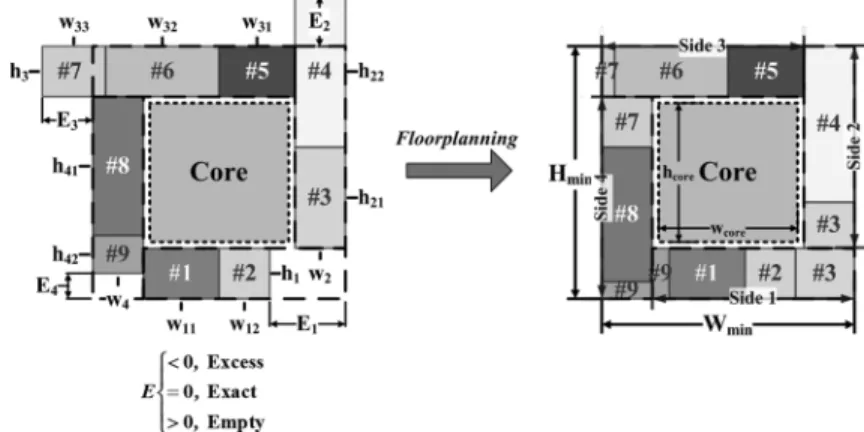
Fig. 8. Minimum package size can be obtained after we designate and floorplan all pin-blocks.
efficiency, routability, and signal integrity for their specific pur-poses by defining their dedicated constraints.
III. FASTPIN-OUTDESIGNATIONAUTOMATION BYPIN-BLOCK
CONSTRUCTION ANDFLOORPLANNING
By using those pin patterns, pin-blocks can be constructed and grouped for pin-out designation. In addition, package size will be minimized by pin-block floorplanning. This section presents the detailed strategies and methodologies. The package size migration issues will be considered in this section as well.
A. Pin-Block Construction and Grouping
In general, designers always take half or one day to define the complete pin configuration for high pin-count chip. It is because the most precise pin configuration will contribute the optimal pin-out and package size in manual design, but it is an exhaustive and time-consuming work. In our approach, the runtime of this manual job can be reduced by a rough pin configuration which simply contains four essential parame-ters: signal-pin name, pin-block placement sequence (order), selected signal-pin pattern, and the number of power-pin, as shown in proposed design flow. First of all, we automatically create the pin-block placement sequence via a simple way. As long as we obtain the rough coordinate of each corresponding component, the pin-block placement sequence will be deter-mined by an intuitive manner of enumerating components clockwise (or counterclockwise). Then, we flexibly design and select an appropriate pin pattern as described in Section II-B.
According to the signal-pin name and selected signal-pin pattern, we can automatically construct all signal-pin blocks by locating signal pins within a block along the specific patterns.
The number of power-pin can be used to deal with the power delivery issue. Our strategy is to establish a power-pin block which can provide a power channel on PCB for various power domains. Designers can freely define the demand of power pins for individual signal configuration relying on the power analysis result. While the signal-pin block is constructed, the proposed automation approach will create power-pin block and place it adjacent to the related signal-pin block, then integrate them into single block for a signal bus. Fig. 8 shows an example, nine pin-blocks ( to ) are constructed for nine different interfaces in a package. Finally, the pin-block placement sequence is applied in pin-block grouping strategies which divide all pin-blocks into four group and place on each package side in the next stage, shown in Fig. 8.
We have further developed two strategies for grouping blocks into package boundaries, the boundary-constrained block grouping strategy (BCPG) and the congestion-free pin-block grouping strategy (CFPG). When we design the pin-out for chipset, which acts as a bridge of all components on moth-erboard, the location of component is one of major constraints presented in Section II-A. Since the locations of components on PCB are boundary-constrained, the grouping strategy BCPG (shown in Fig. 9) will be applied. We defined the safe range for this method
Fig. 9. Boundary-constrained pin-block grouping strategy (BCPG): all pin-blocks will be grouped into single block in proper order until the integrated block size locate within the safe range. The size of grouped pin-block (a) and (b) are closed to each other by adopting BCPG. The disadvantage of this method is that it possibly causes the dense routing likes (b).
Fig. 10. Congestion-free pin-block grouping strategy (CFPG): the first prior consideration is to equalize the signal-pin number. The signal-pin number of grouped pin-block (a) and (b) are very closed after adopting CFPG. The disadvantage of this method is that the locations of PCB components must be restricted and referred to final pin-out.
where is the size of grouped block, and are
user-de-fined parameters, is the average block
size and is the width of each block. Equation (9) shows that the main concern of this methodology is pin-block size. According to the pin-block placement sequence determined in pin configuration, the pin-blocks will be grouped into single block in proper order until the integrated block size locate within the safe range. For this strategy, the size of each grouped block is closed to the average block size then result in mini-mized value (shown in Fig. 8) on each side. Therefore, this method will speed up the runtime of minimizing package size. However, the BCPG will introduce the possibility of generating a dense net-routing due to the disregard of signal-pin number. As shown in Fig. 9, the two grouped pin-blocks (one is grouped
with block 1 and 2, the other is grouped with block 3–5) have closed block width, but they have very different signal-net number. The worse case shown in Fig. 9(b) will decrease the routing efficiency on PCB layout and increase the implemen-tation cost for PCB.
The another strategy is CFPG whose primary consideration is to equally distribute signal-pins on each package side. Con-sequently, the PCB layout will effortlessly lead to a loose den-sity and have more flexibility to match the impedance of critical nets or adjust the location of components. Fig. 10 shows an ex-ample, the signal-pin number of integrated blocks will be close to each other when we adopt CFPG strategy. Therefore, this method is suitable for the package design of field-programmable gate array (FPGA) which has the prior concern of routability.
For CFPG, it will consider the signal-pin number instead of the placement order or side of each pin-block, hence the locations of PCB components will be determined after it accomplishes the final pin-out. The safe range used for this strategy is also defined as follows:
(10) where is the total signal-pin number of grouped block,
and are user-defined parameters, is the
average signal-pin number and is the signal-pin number of each block. Since the equalized signal-pin number is usually larger than the size of grouped block, the second method must has tighter safe range (e.g., ) to achieve the same boundary range as that of the first one.
To implement the strategies of BCPG and CFPG, because the pin-block placement sequence will be considered primarily in BCPG, we will use the first-fit heuristic algorithm which is an approximation algorithm for solving bin-packing problem to group pin-blocks. This algorithm sequentially assigns objects into the first bin, and then creates a new bin when the cur-rent bin is full. For CFPG, the first prior consideration is to equalize the signal-pin number. Therefore, we can apply another bin-packing approximation, the best-fit heuristic algorithm, to group pin-blocks. This heuristic ignores the order of objects and fills all objects into the feasible bins, which have the smallest residual capacity.
From the observations in Section II, signal integrity, power delivery and routability issues should be accounted for in gen-eral cases when signal pins are placed. After finishing the imple-mentation and placement of all blocks, a rough pin designation can be obtained, shown in Fig. 8. At the same time, to can be evaluated from this rough pin designation ( to repre-sent the width or height of the empty and excess area in each side of minimum package). These values will be used for package size minimizing and pin-block floorplanning in Section II-B.
B. Package Size Minimization and Pin-Block Floorplanning
The next step is to optimize package size and acquire a fea-sible pin designation. The objective function and constraints are formulated as a linear program and shown in the following.
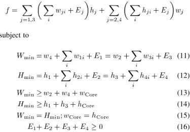
Minimize subject to (11) (12) (13) (14) (15) (16)
where , , , , , , , can be evaluated in the previous step, all shown in Fig. 8. The is the center area of BGA package. In principal, the power and ground pins are lo-cated at the center of package and the die is lolo-cated upon these power and ground pins. As a result, the heat generated from the die can be transferred out through these pins [1]. Thus increasing more power and ground pins located at the center area will im-prove heat dissipation but enlarge the area of , thereby en-large the package size. We use (13) to (14) to define the area of in accordance with physical die size, where and are user specified parameters. If these two values are not given by designer the minimum size can also be obtained when the minimum package size is evaluated. Constraint (11), (12), and (15) will restrict the shape of package to be square. The purpose of (16) is to insure that the minimum package size can accommodate all pin-blocks with almost no void pin positions. After to are obtained, we can easily recognize the posi-tion of the empty and excess area in the minimum package. The final step of proposed methodology is to floorplan pin-blocks, which are to split the pin-blocks in the excess area and fill them into the adjacent empty area. It can completely eliminate exceed area and keep those pins being located around the particular region restricted in previous step. The algorithm of pin-block floorplanning is shown as follows:
1) , // start from side 1
2) , iff ; , iff
3) repeat:
4) while ( ) do
5) if
6) shift pins clockwise // fill the pin-block into empty area in last side until the is zero
7) ,
8) else
9) shift pins counter clockwise // split the pin-block in excess area then group it into next side
10) ,
11) // check next side
12) until all values are large than or equal to zero
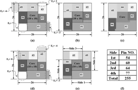
Fig. 11 shows an example, where there are two excess areas occurred in second and third side (upper right and upper left corners) and two empty areas occurred in first and fourth side (bottom right and bottom left corners). According to our algo-rithm, the pin-blocks located in side 1 will be skipped due to (line 4 in the above algorithm). While it considers the pin-blocks of side 2 [see Fig. 11(a)], some of the pins in group will be clockwise filled into the empty area in side 1 ( , line 5 and 6), and then it will consider the pin-blocks in next side. In side 3 [see Fig. 11(b)], because of the pins of group which excess the range of the side will be split and grouped into side 4 (line 8 and 9). Finally, in the last side the pins of group are the same case as that of group [see Fig. 11(c)] and will be floorplanned into the proper locations then acquire an optimized pin-block floorplanning [see Fig. 11(d)] through this simple procedure.
Fig. 11. Example of pin-block floorplanning. The pins in the excess areas will be shifted into the empty areas through our floorplanning algorithm. A final out can be acquired after finishing the package size minimization and pin-block floorplanning.
C. Dealing With Package Size Migration Issues
For practical application, designer usually need to migrate package size from larger to smaller or vice-versa. During chip prototyping, the extra I/O pins are required for monitoring test signals, and then the package size will be dynamically migrated to a larger one. In addition, when the products have cost margin for improving performance or adding the new features, the chip size and package size must be enlarged simultaneously. These requirements can be satisfied easily by changing types of pin pattern from higher (signal-pin number per pattern) to lower one, which increasing the width of pin-blocks. On the contrary, when the cost issue has higher priority then signal integrity or the die size has to be shrunk due to the removal of some features, the package size must be shrunk at the same time. Consequently, the types of pin pattern should be modified from lower to higher one, which increased the efficiency of pin designation but relaxed the performance constraints to acquire smaller pin-blocks.
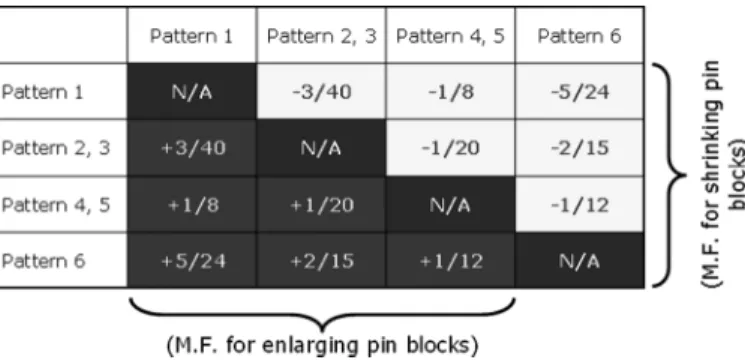
To tackle these package size migration issues, we have defined a migration factor ( ) to evaluate the enlarged or shrunk column number (width) of pin-blocks during changing types of pin pattern. The migration factor can be simply calcu-lated through the following equation:
for enlarging package
for shrinking package (17) where is the given column number of pin pattern, and are the signal-pin number per pattern in previous pattern type and modified pattern type. Fig. 12 shows the migration fac-tors of six patterns proposed in this paper, where “ ” means
Fig. 12. Enlarged and shrunk migration factor (M:F:) of six proposed pin pat-terns, designer can decide the modified pattern along these factors.
TABLE II
TWOINDUSTRIALBENCHMARKSUSED INTHISPAPER
TABLE III
EXPERIMENTALRESULTS OFCASE1ANDCASE2
enlarged factor and “ ” means shrunk factor. Therefore, the total pin number of a group multiplied by the migration factor will estimate the modified width of a pin-block. And then de-signer can decide which pattern should be modified along these estimations.
IV. EXPERIMENTALRESULTS
We have implemented our methodology in C++ and the platform is on AMD Sempron 1.75 GHz with 1 GB memory. We use two industrial mass production chipset cases as our benchmarks, the rough pin configuration charts are shown in Table II. Table III, Figs. 14, and 16 show the results of pin-out designation for these two benchmarks. Based on Table III which is obtained from linear programming formulation shown in Section III-B, we can get corresponding parameters to floorplan all pin-blocks. The runtime of designating pin-out is less than 5 s for both cases. For Case 1, when the BCPG strategy is adopted we can obtain very closed pin-block sizes in first and third side [see Fig. 13(a)] and a rough pin-out in minimum package size [see Fig. 14(a)]. Fig. 14(b) shows our
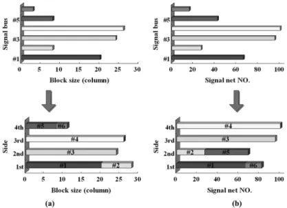
Fig. 13. Pin-blocks grouping results of Case 1: (a) Grouping with BCPG, where the block sizes are very closed in side first and third ( = 0:5, = 1:5). (b) Grouping with CFPG, where the pin number are equalized for all sides ( = 0:8, = 1:2).
Fig. 14. Experimental results of Case 1: (a) Placement of blocks which are grouped with BCPG in minimum package evaluation. (b) Sketch of pin-out after (a) has been floorplanned. (c) Manually designated pin-out. (d) Placement of blocks which are grouped with CFPG in minimum package evaluation. (e) Sketch of pin-out after (d) has been floorplanned. (f) The equalized signal-pin number chart. By using BCPG to group pin-block, our approach can produce the same dimensions as in manual design. The equalized signal-pin number can also be obtained when CFPG is adopted.
final pin-out designation is perfectly matched with manual design [see Fig. 14(c)] achieved by an experienced engineer, which spent long turn-around time to respin the design (usually weeks). By using CFPG strategy, we can equally distribute signal-pins on each side of package [see Fig. 13(b)], even though the pin-blocks need to be floorplanned [see Fig. 14(e)] the variation of signal-pin number is restricted [see Fig. 14(f)]. For Case 2, the same flow as that in case 1 we choose BCPG strategy to group pin-block first [see Figs. 15(a) and 16(a)]. Due to more pin numbers in some buses and signal-pin block pattern usage [while pin number is not divisible by 8 for pattern (1), 10 for pattern (2) and (3), 12 for pattern (4) and (5), 6 for pattern (6) will generate void position, respectively], a slightly larger package size [see Fig. 16(b)] is achieved, but still very
close to the manual design [see Fig. 16(c)]. Next, we use CFPG method to group pin-block [see Fig. 15(b)], the final pin-out [see Fig. 16(e)] shows the signal-pin number in each side of package is very closed to each other [see Fig. 16(f)]. In addition to these two cases, we have tested a case which has 25 groups and 720 signal-pins, the runtime is still below 5 s and obtain the minimum package size as well.
In package size migration cases, we keep using those two industrial cases as the examples. By (17), we can first calculate the as shown in Fig. 12. Then, we multiply pin number in case 1 and case 2 by the to obtain the results of Table IV. This table shows the enlarged or shrunk column number of pin-blocks when we are changing types of pin pattern for all groups in case 1 and case 2. For example, if we want to enlarge package
Fig. 15. Pin-blocks grouping results of Case 2: (a) Grouping with BCPG, where the block sizes are very closed in side first, second, and third ( = 0:5, = 1:5). (b) Grouping with CFPG, where the pin number are equalized for all sides ( = 0:8, = 1:2).
Fig. 16. Experimental results of Case 2: (a) Placement of blocks which are grouped with BCPG in minimum package evaluation. (b) Sketch of pin-out after (a) has been floorplanned. (c) Manually designated pin-out. (d) Placement of blocks which are grouped with CFPG in minimum package evaluation. (e) Sketch of pin-out after (d) has been floorplanned. (f) The equalized signal-pin number chart. When we use BCPG to group pin-block, our approach can produce a pin designation layout (312 31) very close to the manual one (30 2 30). The signal-pin number is very closed to each other by using CFPG strategy.
size of case 1 from 26 26 (mm) to 30 30 (mm), we will need enlarged column number in pin-blocks. We can change the types of pin pattern in bus to and into first, second, or third pattern, which have good signal integrity to gain better performance. On the other hand, when we are trying to shrink package size of case 2 from 31 31 (mm) to 25 25
(mm), the shrunk column number will be .
The only one choice is to change types of pin pattern in bus to into sixth pattern. Since the most selected pin patterns have higher pin designation efficiency in this case. The margin
of enlarging package size will be larger than that of shrinking package size.
V. CONCLUSION
We have proposed a novel and very efficient approach to automating pin-out designation in flip-chip BGA packaging for package-board codesign. Due to the tradeoff in signal perfor-mance and package cost, conventional approach usually takes weeks to modify package size and to rework package substrate
TABLE IV
ENLARGED ORSHRUNKCOLUMNNUMBER OFPIN-BLOCKSWITHMODIFIEDTYPES OFPINPATTERN INCASE1ANDCASE2
and PCB layout, and to rearrange pin-out. Those time-con-suming works can be replaced by our efficient methodology. By considering signal integrity, power delivery, and routability in pin-out block design, our framework provides good signal quality while achieving close-to-minimum package size, which reduces package cost. Finally, the flexibility of package size migration will be preserved by a quick and simple estimation.
ACKNOWLEDGMENT
The authors would like to thank the anonymous reviewers for providing precious comments that greatly improved this paper.
REFERENCES
[1] Altera Corp., “Designing with high-density BGA packages for Altera devices,” Appl. Note AN-114-4.0, Feb. 2006.
[2] H. N. Brady, “An approach to topological pin assignment,” IEEE Trans.
Comput.-Aided Des. Integr. Circuits Syst., vol. 3, no. 7, pp. 250–255,
Jul. 1984.
[3] H.-M. Chen, I.-M. Liu, D. Wong, M. Shao, and L.-D. Huang, “I/O clus-tering in design cost and performance optimization for flip-chip de-sign,” in Proc. IEEE Int. Conf. Comput. Des., 2004, pp. 562–567. [4] S.-S. Chen, W.-D. Tseng, J.-T. Yan, and S.-J. Chen, “Printed circuit
board routing and package layout codesign,” in Proc. IEEE Asia-Pac.
Conf. Circuits Syst., 2002, pp. 155–158.
[5] T.-O. Chong, S.-H. Ong, T.-G. Yew, C.-Y. Chung, and R. Sankman, “Low cost flip chip package design concepts for high density I/O,” in Proc. IEEE Electron. Components Technol. Conf., 2001, pp. 1140–1143.
[6] E. Diaz-Alvarez and J. Krusius, “Design, simulation, fabrication, and characterization of package level micro shielding for EMI/EMC man-agement in BGA environment,” in Proc. IEEE Electron. Components
Technol. Conf., 2000, pp. 793–798.
[7] S. Hall, G. Hall, and J. McCall, High-Speed Digital System Design. New York: Wiley-Interscience Publication, 2000.
[8] R.-J. Lee, M.-F. Lai, and H.-M. Chen, “Fast flip-chip pin-out designa-tion respin by pin-block design and floorplanning for package-board codesign,” in Proc. IEEE Asia South Pac. Des. Autom. Conf., 2007, pp. 804–809.
[9] J. Mcgrath, “Chip/package co-design: The bridge between chips and systems,” Adv. Packag., Jun. 2001 [Online]. Available: http://ap. pennnet.com/display_article/103319/36/ARTCL/none/none/1/Chi p/package-co-design/).
[10] N. Oka, C. Miyazaki, T. Uchida, and S. Nitta, “Effect of a shielding plane connected to ground plane of a PCB in EMI reduction,” in Proc.
Int. Symp. Electromagn. Compatibility, 1999, pp. 204–207.
[11] T. Sudo, Y. Ko, S. Sakaguchi, and T. Tokumaru, “Electromagnetic radiation and simultaneous switching noise in a CMOS device pack-aging,” in Proc. IEEE Electron. Components Technol. Conf., 2000, pp. 781–785.
[12] J. Xiong, Y.-C. Wong, E. Sarto, and L. He, “Constraint driven I/O plan-ning and placement for chip-package co-design,” in Proc. IEEE Asia
South Pac. Des. Autom. Conf., 2006, pp. 207–212.
[13] M.-F. Yu and W.-M. Dai, “Single-layer fanout routing and routability analysis for ball grid arrays,” in Proc. IEEE/ACM Int. Conf.
Comput.-Aided Des., 1995, pp. 581–586.
Ren-Jie Lee (S’07) received the M.S. degree in
electronics engineering from Feng Chia University, Taichung, Taiwan, in 2000. He is currently pursuing the Ph.D. degree in the Department of Electronics Engineering, National Chiao Tung University, Hsinchu, Taiwan.
From 2000 to 2006, he had worked as a Project Manager for Silicon Integrated Systems (SiS) Corpo-ration, Hsinchu Science Park, Hsinchu, Taiwan. His research interests include beyond die-integration and package/hybrid/board design automation which in-clude Chip-Package-Board codesign, System-in-Package design, and analysis and optimization beyond the die.
Hung-Ming Chen (M’04) received the B.S. degree
in computer science and information engineering from National Chiao Tung University, Hsinchu, Taiwan, in 1993, and the M.S. and the Ph.D. degrees in computer sciences from University of Texas at Austin, in 1998 and 2003, respectively.
He is currently an Associate Professor with the De-partment of Electronics Engineering, National Chiao Tung University, Hsinchu, Taiwan. His research in-terests include EDA (nanometer physical design and design methodology), beyond die-integration, design and analysis of algorithms and optimizations.
Dr. Chen has been a member of some technical committees, including IEEE SOCC, ASP-DAC, and VLSI-DAT.