國 立 交 通 大 學
電子工程學系 電子研究所碩士班
碩 士 論 文
多晶鍺奈米線薄膜電晶體與無接面多晶矽
奈米線場效電晶體製作與特性分析
A Study on the Fabrication and
Characterization of Poly-Ge NWTFTs and
Junctionless Poly-Si NWFETs
研 究 生:劉禹伶
指導教授:林鴻志 博士
黃調元 博士
多晶鍺奈米線薄膜電晶體與無接面多晶矽
奈米線場效電晶體製作與特性分析
A Study on the Fabrication and
Characterization of Poly-Ge NWTFTs and
Junctionless Poly-Si NWFETs
研 究 生:劉禹伶
Student:Yu-Ling Liou
指導教授:林鴻志 博士 Advisors:Dr. Horng-Chih Lin
黃調元 博士
Dr. Tiao-Yuan Huang
國 立 交 通 大 學
電子工程學系 電子研究所碩士班
碩 士 論 文
A Thesis
Submitted to Department of Electronics Engineering & Institute of Electronics College of Electrical and Computer Engineering
National Chiao-Tung University in Partial Fulfillment of the Requirements
for the Degree of Master of Science
in
Electronic Engineering December 2010
Hsinchu, Taiwan, Republic of China
i
多晶鍺奈米線薄膜電晶體與無接面多晶矽
奈米線場效電晶體製作與特性分析
研究生 : 劉禹伶 指導教授 : 林鴻志 博士
黃調元 博士
國立交通大學
電子工程學系 電子研究所碩士班
摘要
在本論文中,我們製作並研究兩種新穎的奈米線元件,多晶鍺奈米線薄膜 電 晶 體 (poly-Ge NWTFTs) 與 無 接 面 多 晶 矽 奈 米 線 場 效 電 晶 體 (JL poly-Si NWFETs)。多晶鍺奈米線薄膜電晶體採用一種先進的邊襯蝕刻技術形成奈米線, 並利用固相結晶法(SPC)將非晶鍺轉換為多晶鍺。利用多閘極(multiple-gated)的 結構,開關電流比可以增加至 104,次臨界擺幅可以改善至 0.64 V/dec。此外, 我們也比較了具有獨立雙閘極(independent double-gated)的多晶鍺奈米線電晶 體在各種模式操作時的特性。 無接面多晶矽奈米線場效電晶體(JL poly-Si NWFETs)利用一種簡單的方法, 同時形成源/汲極與通道,且不需要離子佈植即可完成。在特性表現方面,無接 面多晶矽奈米線場效電晶體擁有較佳的操作電流與更低的串連電阻。此外,增 強型(IM)奈米線場效電晶體在特定操作條件下展現出低於 60m V/dec 的次臨界 擺幅。ii
A Study on the Fabrication and
Characterization of Poly-Ge NWTFTs and
Junctionless Poly-Si NWFETs
Student : Yu-Ling Liou Advisors : Dr. Horng-Chih Lin
Dr. Tiao-Yuan Huang
Department of Electronics Engineering and Institute of Electronics
National Chiao Tung University, Hsinchu, Taiwan
Abstract
In this thesis, two kinds of nanowire devices, namely, poly-Ge nanowire thin
film transistors (NWTFTs) and junctionless (JL) poly-Si nanowire field effect
transistors (NWFETs) were fabricated and investigated. Poly-Ge NWTFTs were
realized with a novel approach by adopting the sidewall spacer etching technique for
NW channel formation. Solid phase crystallization (SPC) was utilized to transform amorphous Ge (α-Ge) to poly-Ge. By adopting multiple-gated structure, ON/OFF current ratio is increased to 104 and subthreshold swing (S.S.) is improved to
0.64V/dec. Besides, poly-Ge NWTFTs with independent double-gated (DG)
configuration are characterized and compared. Each gate can be biased
independently to manipulate the device.
iii
the source/drain (S/D) and channel was formed simultaneously without implantation.
JL devices show better on-state performance and lower series resistance. On the
other hand, the inversion mode (IM) NWFETs present ultra-low S.S. lower than
iv
Acknowledgement
首先我要感謝我的指導教授,林鴻志博士與黃調元博士,感謝林老師,讓我 學習到嚴謹的研究態度,也指導我元件分析的觀念。感謝黃老師專業領域上豐富 的知識,以及精湛的文學造詣,使我獲益良多。感謝蘇俊榮博士,謝謝你不厭其 煩的與我討論數據,給予我很多正確的觀念,幫助我順利完成第二個題目。 接著要感謝實驗室的學長學姊們。感謝蔡子儀學長,在實驗上幫了我太多的 忙,也很感謝你私底下給我很多的關心與幫助,也因為你我這宅女才會出門走走, 還有謝謝你的咕咪。感謝陳威臣學長,很有耐心的帶著我做實驗,並且給予我很 多寶貴的經驗與實驗設計的想法,幫助我完成鍺魔王的題目。感謝徐行徽學長, 謝謝你的關心與照顧,每天的生活都很充實。感謝林哲民學長,暑假陪我做了一 批五味雜陳的貨,也謝謝你在我論文上給我點子與觀念,幫助我畢業。感謝郭嘉 豪學長,感謝李克慧學姊,你們都很有博士班學長姊的風範,謝謝你們。 還要感謝同屆的同學,謝謝許家維、羅正瑋、林庭輔、陳冠宇、簡敏峰、張 博翔。謝謝許家維,聽我碎碎唸,在各方面也幫了我很多的忙,從你身上也學習 到做研究的態度。謝謝羅正瑋的關心,也教了我很多東西,你真的是個很有耐心 且細心的人,你對課業與實驗的精神也讓我相當欽佩。謝謝林庭輔,常常發生有 趣的事情,帶給實驗室歡樂,也謝謝你畢業之後還會跟我聊聊。謝謝陳冠宇,陪 我在 Ge 的世界載浮載沉。謝謝簡敏峰,你渾然天成的宅氣與資深酸民功力真的 讓我開了眼界,很有趣。真的很感謝同屆的同學,讓我覺得 631 是一個開心的地 方,與你們相處真的很快樂也學了很多,謝謝你們畢業之後還是關心我的進度與 近況,能與你們當同學真的很幸運。 感謝實驗室的學妹們,謝謝林歷樺、余曉惠、張維真、彭梵懿,妳們都很有 活力,與妳們聚在一起聊聊也很開心,也感謝蘇段凱學弟幫了我很多的忙,祝福 你們往後的實驗與研究都很順利。 劉禹伶 誌於 風城交大 2010 年 12 月v
Contents
Abstract (Chinese)………... i Abstract (English)………... ii Acknowledgement (Chinese)……….. iv Contents……… vList of Figure Captions………... vii
List of Table Captions………. xi
Chapter 1 Introduction
1-1 Evolution of Nanowire Technology……… 11-2 Germanium Material Properties and Devices………... 3
1-3 Overview of Multiple-gated Transistors………... 4
1-4 Overview of Junctionless MOSFET………... 5
1-5 Motivation………... 6
1-6 Thesis Organization……….... 6
Table Captions………... 8
Chapter 2 Poly-Ge NWTFTs
2-1 Samples Preparation……… 92-2 Device Structure, Fabrication and Measurement……… 11
2-2.1 Process Flow of Single Side-Gated and Inverse-T-Gated Poly-Ge NWTFTs………...…... 11
2-2.2 Process Flow of Independent Double-Gated Poly-Ge NWTFTs………. 12
2-2.3 Measurement Setup……….. 12
vi
2-4 Electrical Characteristics of Independent Double-gated Poly-Ge NWTFTs... 14
2-4.1 Fundamental Electrical Characteristics……… 14
2-4.2 Threshold Voltage Modulation………. 15
2-5 Brief Summary……….... 16
Table Captions………... 18
Chapter 3 Junctionless Poly-Si NWFETs
3-1 Device Structure and Fabrication……….... 193-1.1 Process Flow of Junctionless Poly-Si NWFETs……….. 19
3-1.2 Process Flow of Poly-Si NWFETs with Undoped Channel....…………. 21
3-2 Measurement Setup………. 22
3-3 Electrical Characteristics of JL and IM Poly-Si NWFETs……….. 23
3-3.1 Fundamental Electrical Characteristics……… 23
3-3.2 Transconductance………... 27
3-4 Series Resistance of JL and IM Poly-Si NWFETs……….. 29
3-5 Observation of Anomalously Low Subthreshold Swing………. 31
Table Captions………... 33
Chapter 4 Conclusion and Future Work
4-1 Conclusion……….. 344-2 Future Work……… 35
References………. 37
Figures………. 44
vii
List of Figure Captions
Chapter 2
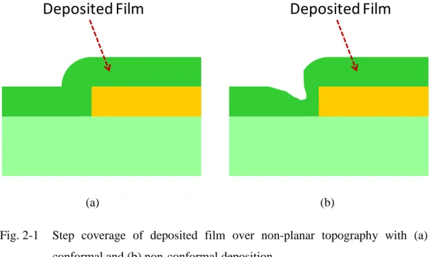
Fig. 2-1 Step coverage of deposited film over non-planar topography with (a)
conformal and (b) non-conformal deposition. .………... 44
Fig. 2-2 SEM images of 100 nm-thickness α-Ge thin films deposited on (a) the single side-gated structure and (b) inverse-T-gated structure. .…………... 45
Fig. 2-3 SEM image of a 150 nm-thickness α-Ge thin film deposited on the single side-gated structure. .………... 46
Fig. 2-4 TEM cross-sectional view of poly-Ge film annealed at 500 oC for 1 hour.
The circled area in the image indicates the region of a grain. .…………... 46
Fig. 2-5 Diffraction pattern of the poly-Ge film. .………. 47
Fig. 2-6 Top views of (a) single side-gated (b) inverse-T-gated poly-Ge NWTFT. . 48
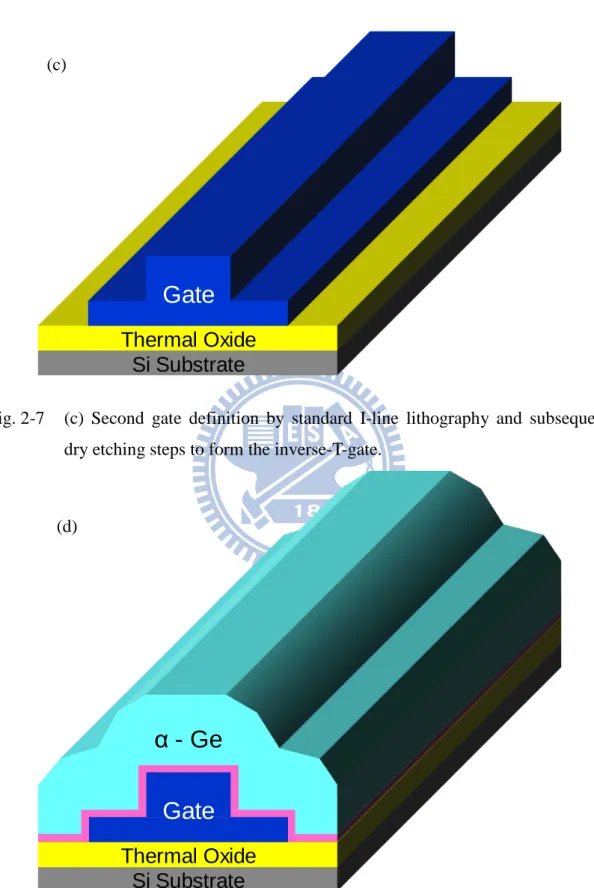
Fig. 2-7 (a) Deposition of in situ doped n+ poly-Si on oxide-capped Si substrate.
(b) First gate definition by standard I-line lithography and subsequent dry
etching steps. (c) Second gate definition by standard I-line lithography
and subsequent dry etching steps to form the inverse-T-gate. (d)
Deposition of gate oxide and α-Ge layers. (e) Source/Drain ion implantation. (f) Definition of source/drain and formation of NW channel. 49
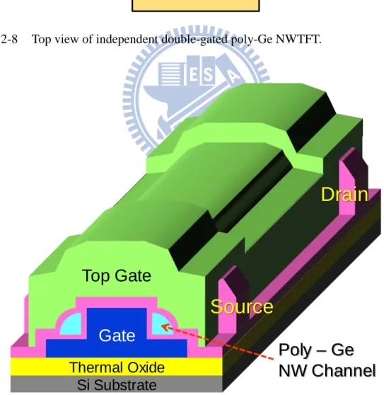
Fig. 2-8 Top view of independent double-gated poly-Ge NWTFT. .……… 52
Fig. 2-9 Deposition of top gate oxide and formation of top gate. .………... 52
Fig. 2-10 SEM picture of a fabricated device. Both height and width of NW channel
are 45 nm. .……….. 53
Fig. 2-11 Comparisons of transfer characteristics between inverse-T-gated and
Single Side-Gated poly-Ge NWTFTs with channel length of (a) 0.4 and (b) 0.7 µm. .………. 54
viii
Fig. 2-12 Output characteristics of ITG and single side- gated poly-Ge NWTFTs. . 55
Fig. 2-13 Comparisons of transfer characteristics between poly-Ge planar TFT and
poly-Ge NWTFT (ITG : inverse-T-gated). .……… 55
Fig. 2-14 Transfer characteristics of independent DG poly-Ge NWTFT operated in
single-gated (SG) modes and double-gated (DG) mode. .………... 56
Fig. 2-15 Output characteristics of a device under DG mode. .……….. 56
Fig. 2-16 Comparisons of output characteristics between DG and SG modes of
operations with gate voltage of (a) -6 V and (b) -9 V. .………... 57
Fig. 2-17 Transfer characteristics of DG devices characterized by sweeping
inverse-T gate voltage with top gate biased at various constant values. .... 58
Fig. 2-18 Extracted Vth as a function of top-gate voltage (ITG: inverse-T-gated). ... 58
Chapter 3
Fig. 3-1 (a) Top view and (b) cross-sectional view of JL poly-Si NWFET. .……... 59
Fig. 3-2 Fabrication of the JL device. (a) Deposition of a bottom nitride/TEOS
oxide/hardmask nitride stacked layer. The thicknesses were 50/30/30 nm,
respectively. (b) The hardmask nitride/TEOS oxide stack was defined by
anisotropic reactive plasma etching. (c) The formation of cavities by
utilizing DHF lateral etching. (d) Deposition of in situ phosphorus doped
poly-Si layer. (e) Definition of source/drain and formation of doped
pol y-Si NW channels. (f) Removal of bottom nitride/TEOS
oxide/hardmask nitride stacked layer. The NW channels are hanging
between the S/D regions. (g) Deposition of a TEOS oxide layer as the
gate dielectric. (h) Deposition of a TiN film as the gate electrode. .……... 59
ix
followed by 600oC annealing at N2 ambient for 24 HR (SPC). (b) Dry
etching to form NWs underneath the hard mask. (c) Deposition of 100 nm
in situ phosphorus doped poly-Si layer. (d) Definition of S/D regions by
dry etching. .……… 63
Fig. 3-4 Cross-sectional-view TEM picture of a JL-NWFET with GAA structure. . 65
Fig. 3-5 Transfer characteristics of (a) JL-NWFETs and (b) IM-NWFETs at VD =
0.1 V. .……….. 66
Fig. 3-6 Measured ION of JL and IM devices as a function of channel length. .…... 67
Fig. 3-7 (a) A schematic diagram illustrating the collapse of the suspended NW
channels after the surrounding dielectrics were removed during
fabrication as the channel length is larger than 1 μm. (b) TEM image of omega-gate. .……… 68
Fig. 3-8 Output characteristics of the JL and IM NWFETs with (a) L = 0.4 μm and (b) L = 5 μm. .……….. 69 Fig. 3-9 Threshold voltage as a function of channel length for (a) JL-NWFETs and
(b) IM-NWFETs. .………... 70
Fig. 3-10 Drain-induced barrier lowering (DIBL) for J L-NWFETs and
IM-NWFETs as a function of channel length. .…..………. 71
Fig. 3-11 The subthreshold swing of (a) JL-NWFETs and (b) IM-NWFETs as a
function of channel length. ……….. 72
Fig. 3-12 Drain current and gate current versus gate voltage for (a) JL-NWFET and
(b) IM-NWFET measured at VD = 0.5 V and VD = 2 V. ……….. 73
Fig. 3-13 The transconductance of devices as a function of gate overdrive voltage
with (a) L = 0.4 μm and (b) L = 5 μm. .………... 74 Fig. 3-14 Subthreshold characteristics and transconductance of JL-NWFET and
x
IM-NWFET versus gate voltage. .………... 75
Fig. 3-15 Subthreshold characteristics and transconductance as a function of gate
overdrive voltage. .………... 75
Fig. 3-16 Comparisons of field-effect mobility for JL-NWFETs and IM-NWFETs. . 76
Fig. 3-17 Extraction of Rtot for JL-NWFETs and IM-NWFETs. ………. 76
Fig. 3-18 Transfer Characteristics with various drain voltages (L= 5 μm). .……….. 77 Fig. 3-19 Extracted Vth and S.S. from Fig. 3-18 as a function of drain voltage. .…... 77
xi
List of Table Captions
Chapter 1
Table 1-I Properties of Si and Ge. .………. 8
Chapter 2
Table 2-I Definition of three operation modes. .………. 18
Table 2-II Comparison of the electrical parameters among various modes of
multiple-gated operations. .………. 18
Chapter 3
Table 3-I The mean values of Ion of JL and IM NWFETs and the current ratio. The
- 1 -
Chapter 1
Introduction
1-1 Evolution of Nanowire Technology
In integrated circuit (IC) industry, it is well known that the size of transistors has
to be scaled down continuously to achieve high operating speed and improved
performance, thereby maintaining the benefit of products in each generation. The
underlying principle for the downscaling of metal-oxide-semiconductor
field-effect-transistor (MOSFET) is Moore’s law [1-1]. In 1965, Gordon Moore
observed that the number of transistors in a chip doubled every two years. As the
feature size of transistor shrinks from deep sub-micrometer to nanometer scale, the
conventional scaling methods of the semiconductor devices encounter increasing
technological and fundamental challenges [1-2].
Recently, various novel devices based on nanostructures, such as nanowire,
nano-ribbon, etc. have been widely proposed and investigated [1-3]. When a
stripe-structured material with a diameter or feature size smaller than 100 nm, it is
termed nanowire. Since nanowire has very tiny volume and large surface-to-volume
ratio, transistors based on nanowire channel can possess better gate control capability
compared to the conventional planar type MOSFETs [1-4]. In addition, nanowire
channel can significantly restrain the short channel effects (SCEs) of transistors. By
ingeniously designing the structure of nanowire devices, the leakage current can be
- 2 -
the aforementioned advantages, nanowires are feasible and promising for several
applications in the future.
Based on the method of preparation, nanowires can be virtually separated into
two classes, one is top-down, and the other is bottom-up [1-6]. In general, IC
manufacturing utilizes the top-down approach, which fabricates devices and
interconnects by standard IC processes such as photolithography, thin-film deposition,
etching, and metallization [1-5]. These techniques are well developed and mature for
mass production purpose. Nevertheless, directly defining the prerequisite nanowire
patterns necessitates very expensive lithography equipments and advanced techniques
such as deep-UV steppers, e-beam writers, or nano-imprint tools [1-7]. Although
cheaper photolithographic processes (e.g., G-line and I-line steppers) are not capable
of patterning nanowires directly, some helpful approaches like thermal flow [1-8],
chemical shrink [1-9], and spacer patterning [1-10] have been proposed to help
generate the nano-scale patterns using these conventional lithography tools. On the
other hand, bottom-up approach is non-lithographic and the key techniques are
chemical synthesis and self-assembly. In bottom-up method, the nanowires are
synthesized through different chemical methods such as vapor–liquid–solid (VLS)
[1-11], surface diffusion and epitaxy [1-12] [1-13], solution–liquid–solid (SLS), and
oxide-assisted growth (OAG) [1-14]. Most commonly, nanowires are synthesized by
using metal-catalyzed VLS method [1-15]. Although this method can be done under
the premise of low cost, and the nanowire diameter defined during the growth or
chemical synthesis process can be controlled with near-atomic-scale precision [1-16],
it still faces repeatability, reliability and reproducibility problems. Moreover, metal
- 3 -
1-2 Germanium Material Properties and Devices
As early as 1947, J. Bardeen, W. Brattain and W. Shockley developed the first
transistor at Bell Laboratory by using germanium (Ge) as the device’s substrate [1-17].
Recently, Ge has regained a considerable amount of interests in research due to its
great potential as active channel materials for nano-scale CMOS transistors [1-18]. As
shown in Table 1-I, Ge has several fascinating properties suitable for electronic
devices. First, the electron and hole mobilities in crystalline Ge are much higher than
that in crystal silicon (Si). This property enables Ge a good candidate as the channel
material for high-speed devices and circuits. In comparison with Si, the mobility
difference in magnitude between electrons and holes in Ge crystal is smaller; hence
Ge has more advantages in design and fabrication of complementary
metal-oxide-Semiconductor (CMOS) with a more symmetrical configuration.
Secondly, Ge has lower melting and crystallization temperature as compared with Si.
For example, the melting point of single crystal Ge is 937 oC, lower than that of Si
(i.e., 1412 oC). Activation of the source/drain dopants can be done at a temperature as
low as 400 ~ 500 oC [1-19]. These features allow Ge to be used in a variety of
applications which demand low temperature processing. In addition, Ge also can be
applied to non-silicon monolithic 3D integrated circuits (3D-ICs) [1-20].
However, applying Ge as device channel in MOSFETs has some daunting
problems. Most higher-mobility materials have a much smaller band gap compared to
Si and suffer from higher band-to-band-tunneling (BTBT) leakage, which may
ultimately limit their scalability [1-21]. Moreover, unlike Si which can directly form
high-quality oxide by high temperature thermal oxidation, the inferior quality of
- 4 -
[1-23]. Fortunately, the recent advancement in the preparation of high-k dielectric
enables the improvement in the characteristics of Ge MOSFETs [1-24] [1-25].
1-3 Overview of Multiple-gated Transistors
When the devices continue scaling down, precise control of critical structural
parameters is a critical problem. For example, for single-gated fully depleted
silicon-on-insulator (FDSOI) devices, the silicon body thickness must be about a third
to a half of the gate length in order to retain good control over SCEs [1-26] [1-27].
However, high uniformity of the ultra-thin channel thickness is a basic requirement
but very difficult to achieve. To relieve this concern, the adoption of multiple-gated
field-effect transistor (MuGFET) structure [1-28] is most popularly taken into
consideration. The MuGFET is a device with more than one side of the channel
wrapped by the gate electrode. Double-gated FinFET, the thickness of the silicon
channel (or the fin) between the two opposite gates is relaxed to approximate one or
two-thirds of the physical gate length since each gate controls half the body thickness
[1-29]. It means that the MuGFET has the ability to relax the physical and process
limitations introduced with gate length scaling.
The double-gated FinFET, triple-gated, pi-gate, omega-gate and gate-all-around
SOI devices all belong to the MuGFET architectures [1-30]. According to the ITRS
roadmap [1-31], the excellent electrostatic control of these devices will be required for
sub-25 nm gate lengths [1-32]. MuGFET devices realize some excellent virtues, such
as great immunity against SCE, good gate controllability and near ideal subthreshold
- 5 -
1-4 Overview of Junctionless MOSFET
A typical MOSFET involves the source-to-channel junction and the
drain-to-channel junction. The junctions are called the PN junctions and consisted of
ultra-sharp doping profile. For example, for a modern n-channel transistor, the source
and drain are doped with n-type dopants at a concentration of 1×10²⁰ atoms/cm3 and
the channel is of p-type doping at a concentration of 1×10¹⁸ atoms/cm3 [1-34]. In very
short-channel devices, the extraordinarily high doping concentration gradient imposes
variation in diffusion of impurities over a distance of a few nanometers. This requires
a very tight thermal budget which shrinks dramatically with device scaling.
Recently, junctionless (JL) MOSFET has been developed to cope with the
above-mentioned issue [1-34][1-35][1-36]. Compared to conventional MOSFET,
JL-MOSFET has no source or drain junctions because the doping type and doping
concentration are the same in the channel, source and drain regions. Since the
constraints in the formation of ultra-shallow junction in conventional CMOSFETs can
be avoided, fabrication process of JL-MOSFET is greatly simplified.
The most important and critical part of this scheme is the conditions of the
semiconductor layer (or channel layer). The channel layer must be thin enough so it
can be fully depleted by the gate to turn off the device. Furthermore, the doping
concentration should be high enough to provide low source/drain resistance and
sufficient driving current when the device is turned on. According to the previous
work in Ref. [1-36], JL-MOSFET with multiple-gated and ultra-thin channel structure
could have nearly ideal subthreshold slope (~ 60 mV/dec) and limited leakage current.
Moreover, it also shows less degradation in mobility with gate voltage and
- 6 -
1-5 Motivation
Our laboratory (Advanced Device Technology Lab) has proposed and developed
a novel technique to fabricate poly-Si nanowire thin-film-transistor (NWTFT) [1-37].
The main advantage is that it does not require expensive equipment, and the
fabrication is simple. The feature size of NWs is determined by the thickness of
deposited film as well as adjusting the etching time in the NW channel defining step.
Besides, NW channel, source and drain can be formed simultaneously and positioned
accurately. The NWs are also free from metal contamination. Finally, our technique
has good reproducibility and reliability.
One of the issues for the above NW device is the limited on-current due to the
use of poly-Si. As described previously, Ge has many advantages, such as higher
carrier mobility, lower melting and crystallization temperatures. These features make
Ge a potential and promising channel material. Besides, the unique junctionless
structure in JL-MOSFETs is also promising to promote the device characteristics. In
this work we exploit the feasibility of using Ge or heavily doped poly-Si as the
channel layer of the NW devices.
1-6 Thesis Organization
In this thesis, several types of NWTFTs equipped with different channel material
were fabricated and characterized, including poly-Ge NWTFTs, n-channel poly-Si
JL-NWFETs and IM-NWFETs. Devices with multiple-gated structure were also
- 7 -
In the first chapter, we briefly introduce the evolution of nano devices and the Ge
material. In Chapter 2, the process flows of poly-Ge NWTFT with different gated
structure including side-gate, inverse-T-gate and inverse-T-double-gate (ITDG) are
depicted. The electrical characteristics of fabricated devices are also shown and
compared. In Chapter 3, junctionless (JL) poly-Si NWFET and inversion mode (IM)
poly-Si NWFET were fabricated and analyzed. Finally, we summarize important
- 8 -
Table Captions
Table 1-I. Properties of Si and Ge [1-38].
Electrical property Si Ge Mobility(bulk) Electron 1500 cm2/V-s 3900 cm2/V-s Hole 450 cm2/V-s 1900 cm2/V-s Band Gap(bulk) Direct ~0.8 eV Indirect ~1.1 eV ~0.66 eV Melting point Tm (°C) 1412°C 937°C
- 9 -
Chapter 2
Poly - Ge NWTFTs
2-1 Samples Preparation
In this section, we will firstly describe the ultrahigh-vacuum (UHV) Ge
sputtering system, and then discuss the material properties of the sputtered Ge. For the
purpose of fabricating Ge-NWTFT, some approaches for alleviating the difficulties
met in device fabrication will also be described.
Sputter deposition is a physical vapor deposition method where thin films are
deposited on substrates via vaporizing a material target. In general, sputter deposition
takes place in a vacuum. In our fabrication, the base pressure in the UHV Ge
sputtering system is 5×10⁻⁸ torr. Such a low base pressure would reduce the
contamination level of impurities (e.g. O) in the deposited films. If the substrate has a
non-planar topography, however, conformity of the deposited film is a concern. Since
the sputter materials typically have a high sticking coefficient and approach the
substrate with directions almost perpendicular to the substrate surface, protruding
features block the sputter material from being deposited in some areas [2-1]. This
phenomenon is called "shadowing", which may lead to poor step coverage (Fig. 2-1)
[2-2].
According to our NWTFT fabrication method [2-3], the NW channel is supposed
- 10 -
conformal thin-film deposition and decent step coverage to achieve NW spacer
formation. In this thesis, however, the Ge channel film was deposited by UHV
sputtering system, so the poor step coverage of Ge film could be a major issue for
device fabrication and needs to be resolved.
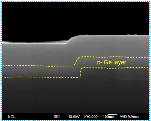
In this experiment, we examined the uniformity of the Ge thin film. In order to form the spacer as NW channel in the etching step, a sufficiently thick α-Ge thin film must be deposited at the sidewalls of the side-gate. The cross-sectional scanning
electron microscopic (SEM) images for samples with nominally deposited film
thickness of 100 nm are shown in Fig. 2-2 (Fig. 2-2(a) for single side-gated structure
and Fig. 2-2(b) for inverse-T-gated structure). It can be seen that the film thickness
reduces as it crosses a step, indicating that the deposited thin film has a poor step
coverage (marked by red circle). To address this issue, we tried to change the thickness of α-Ge deposition from 100 nm to 150 nm. In Fig. 2-3, we can see a better step coverage is resulted with such thicker film. Base on this result, thickness of 150
nm was chosen for α-Ge deposition in this study.
Moreover, in order to transform α-Ge into polycrystalline state for better crystal property, solid-phase crystallization (SPC) is employed as the recrystallization method.
In the previous works [2-4], the sample preparation and recrystallization temperature
of SPC process for poly-Ge were investigated and discussed. The transmission
electron microscopy (TEM) image and diffraction pattern of the poly-Ge film
annealed at 500 oC for 1 hour are shown in Fig. 2-4 and Fig. 2-5, respectively. From
the TEM analysis, the grain size is about 5 nm, while the diffraction pattern shows
that the Ge film has been transformed into poly-Ge, which is in agreement with the
XRD profile. For this reason, in the device fabrication described below, the annealed
- 11 -
2-2 Device Structure, Fabrication and Measurement
2-2.1 Process Flow of Single Side-Gated and Inverse-T-Gated
Poly-Ge NWTFTs
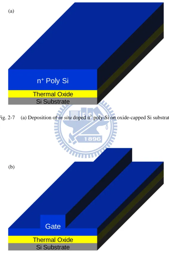
Top view of single side-gated device and inverse-T-gated device are given in Fig.
2-6. Figs. 2-7(a) to (f) show the stereograph and process flow of the proposed
inverse-T-gated device. First, silicon wafers were capped with a 200 nm-thick thermal
oxide layer. After depositing a 150 nm-thick in situ doped n+ poly-Si (Fig. 2-7(a)), the
inverse-T-gate was formed by applying twice the standard I-line lithography and dry
etching steps (Figs. 2-7(b) and (c)). Then, 30 nm tetraethyl orthosilicate oxide
(TEOS-SiO2) was deposited by low-pressure chemical vapor deposition (LPCVD) as
the gate dielectric. After standard cleaning, a 150 nm-thick α-Ge film was deposited on the SiO2 through the UHV Ge sputtering system (Fig. 2-7(d)). Subsequently,
source/drain (S/D) implant was performed by BF2+ implantation with a dose of 5×10¹⁵
cm-2 at 40 keV (Fig. 2-7(e)). After forming S/D photoresist patterns through I-line
stepper, a reactive plasma etching step was employed to form the NW channels
simultaneously with S/D definition. During the etching process, the two NW channels
were precisely positioned abutting the upper stud of the inverted-T-gate in a
self-aligned manner (Fig. 2-7(f)). Then, 30 nm PECVD TEOS oxide capping layer was deposited. Next, to transform the α-Ge layer into poly-Ge, a solid-phase crystallization (SPC) treatment was executed at 500 oC for 1 hour in N2 ambient.
Finally, all devices were then capped with a 220 nm-thick oxide passivation layer.
Fabrication of single side-gated devices is basically the same as that of the
- 12 - one time lithographic step for patterning.
2-2.2 Process Flow of Independent Double-Gated Poly-Ge
NWTFTs
Top view of independent double-gated poly-Ge NWTFT is given in Fig. 2-8. The
process flow and fabricated structure are similar to that described in 2-2.1. The only
difference is the formation of an additional top gate after definition of the S/D and
NW channels. The top gate was made up of a 300 nm-thick aluminum (Al) which was
deposited by electron-beam evaporation system after the deposition of PECVD top
gate oxide on the NW channels. Then Al top gate was defined by I-line lithography
and patterned by dry etching (Fig. 2-9). Finally, a 220-nm-thick passivation layer was
deposited.
2-2.3 Measurement Setup
The transfer characteristics and output characteristics of the fabricated devices in
this thesis were measured by a Keithley 4200 semiconductor characterization system
with Keithley Interactive Test Environment (KITE) software and HP4156
semiconductor parameter analyzer and Interactive Characterization Software (ICS)
program. In all measurements, the temperature was controlled at a stable value by
temperature regulated hot-chuck.
According to the ID-VG curve measured at VD = -0.5 V, threshold voltage (Vth)
- 13 -
current method and defined as the gate voltage (VG) needed to achieve a specific drain
current (ID). The expression is as follows,
th G
@
D10
W
V
V
I
nA
L
=
=
×
(Eq. 2-1)where W and L are the channel width and length, respectively. S.S. is calculated from
the subthreshold current in the weak inversion region, given by,
(
)
. .
log
G DV
S S
I
∂
=
∂
(Eq. 2-2)Moreover, for the ON/OFF current ratio (ION/IOFF), ION and IOFF are determined from
the ID-VG curves, where ION is chosen as the maximal ID and IOFF is the minimal one.
2-3 Electrical Characteristics of Poly-Ge NWTFTs
The cross-sectional SEM image of a poly-Ge NWTFT is shown in Fig. 2-10. The
cross-sectional dimension of the poly-Ge NW is around 45 nm.
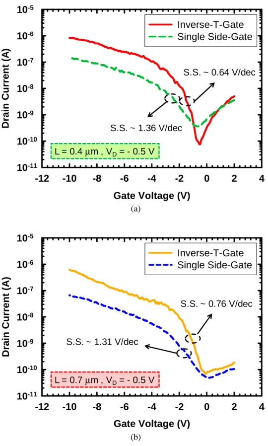
The transfer characteristics of poly-Ge NWTFTs with single side-gated and
inverse-T-gated structure are given in Fig. 2-11. Channel length (L) = 0.4 μm in Fig. 2-11(a) and 0.7 μm in Fig. 2-11(b). Both the fabricated devices show decent transistor characteristics with ~2.5×10² ON/OFF current ratio for single side-gated device, and
~104 for inverse-T-gated split. In Fig. 2-11(a), the S.S. of single side-gated device is
1.36 V/dec, and for inverse-T-gated device it is 0.64 V/dec. The Vth of single
side-gated device is -2.09 V, and for inverse-T-gated device it is -1.56 V. Apparently,
- 14 -
current and steeper subthreshold slope. This is mainly attributed to the fact that the
inverse-T-gated NW device has larger gated area and thus possesses better gate
control capability as compared to the single side-gated device. The output
characteristics of single side-gated and inverse-T-gated poly-Ge NWTFTs are also
shown and compared in Fig. 2-12. The results again show that the inverse-T-gated
poly-Ge NWTFT exhibits better device performance.
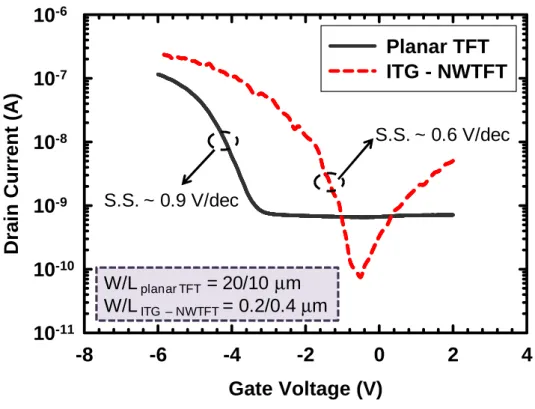
Furthermore, the transfer characteristics of the poly-Ge NWTFT and the poly-Ge
planar TFT are compared in Fig. 2-13. Channel width and length of two types of
devices are shown in the figure. For poly-Ge NWTFT, the S.S. is 0.6 V/dec and the
Vth is -1.80 V. For poly-Ge planar TFT, the S.S. is 0.9 V/dec and the Vth is -4.17 V.
Obviously, the NW device shows better S.S., smaller Vth and reduced Imin in spite of
the much shorter channel length (0.4 μm) over that of the planar one (10 μm).
2-4 Electrical Characteristics of Independent
Double-gated Poly-Ge NWTFTs
2-4.1 Fundamental Electrical Characteristics
In Sec. 2-3, the devices characterized are with only one gate electrode that the
gate bias can be applied to for device characterization. In this section, poly-Ge
NWTFTs with independent double-gated (DG) configuration are characterized and
compared. Each gate can be biased independently to manipulate the device. Such
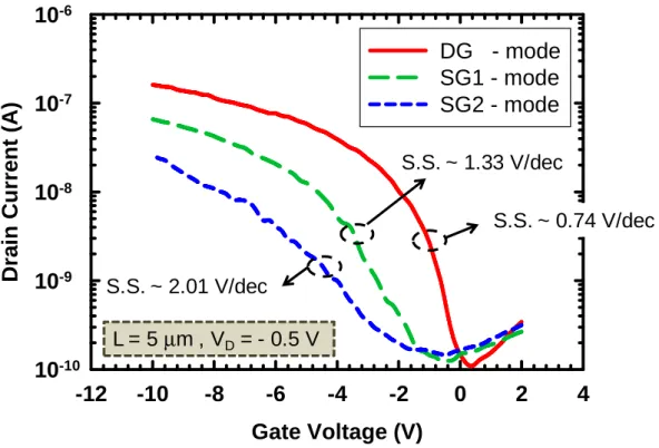
design allows more freedoms for device operation [2-5]. Three operation modes
- 15 -
SG-2) and one double-gated (DG) modes. The SG modes, namely, the sweeping gate
voltage is applied to one of the two gates (the driving gate), while the other gate is
grounded during the measurement. For the DG mode, both the inverse-T gate and top
gate electrodes are connected together and applied simultaneously with the sweeping
voltage.
Typical transfer characteristics under SG and DG modes are shown in Fig. 2-14.
Due to the stronger gate controllability over the NW channels, the DG mode exhibits
significantly better performance as compared to the two SG modes, such as lower Vth,
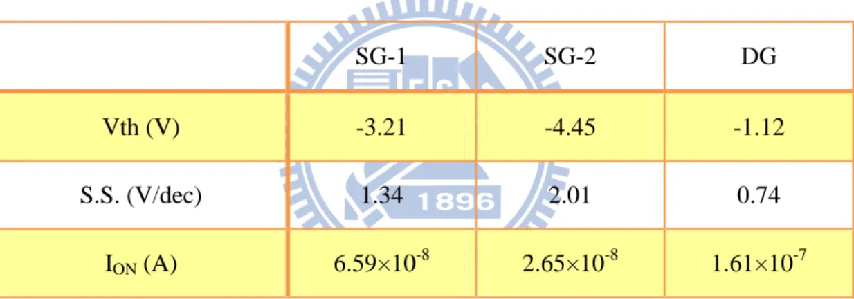
steeper S.S. and higher ION. Moreover, due to larger gated area, operating under SG-1
mode shows better performance than SG-2 mode. For SG modes, the remaining gate
is grounded throughout the measurements, so the three curves have a common
intersection point while the gate voltage is zero. Some representative electrical
parameters are summarized in Table 2-II.
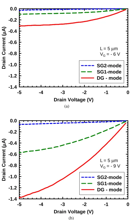
Output characteristics are shown in Fig. 2-15 and Fig. 2-16. In Fig. 2-15, devices
are operated under DG-mode. In Figs. 2-16(a) and (b), the drain voltages are -6 V and
-9 V respectively. The performance of DG mode clearly outperforms the others.
2-4.2 Threshold Voltage Modulation
In this measurement, the sweeping voltage is applied to the inverse-T-gate, while
a fixed voltage varying from +2 V to -6 V in -2 V step is applied to the top-gate. Fig.
2-17 shows the transfer characteristics of the independent double-gated device with
inverse-T-gate as the drive gate and the top gate as the Vth control gate. In Fig. 2-17,
- 16 -
represents the transfer characteristics under DG mode of operation. Obviously, the
curve is shifted with the sweeping voltage, and the Vth could be flexibly controlled by
the top-gate bias. The reason for this phenomenon is due to the tiny NW channels, in
which the entire channel potential can be easily modulated by either inverse-T-gate or
top-gate, leading to conspicuous gate-to-gate coupling effect.
Extracted Vth data is depicted in Fig. 2-18. Although the Vth from the transfer
curves are not linearly modulated by the top-gate, the Vth shift clearly reveals this
trend. The flexible Vth controllability of double-gated TFTs could be used to resolve
the stand-by power consumption issues [2-5]. For instance, as the circuit is operated in
stand-by mode, the Vth can be adjusted to a higher value to suppress the subthreshold
leakage current and thus the power consumption. In contrast, an adequate driving
current can be obtained in active mode by adjusting Vth to a lower value.
2-5 Brief Summary
We proposed a new field-effect transistor structure which utilizes poly-Ge
nanowire (NW) as the channels. In comparison with single side-gated structure,
inverse-T-gated achieved better performance in terms of higher ON/OFF current ratio
and steeper subthreshold swing, owing to the fact that the inverse-T-gated NW device
possesses better gate control capability as compared to the single side-gated device.
Besides, poly-Ge NWTFTs with independent double-gated (DG) configuration
are characterized and compared. Each gate can be biased independently to manipulate
- 17 -
In fact, the grain size of poly-Ge recrystallized by SPC method in our device is
very small (< 5 nm). This means that many defects are contained in the channel layer
or near the interface between poly-Ge channel and gate oxide, leading to performance
degradation. Enhancement in film crystallinity is essential for boosting the device
- 18 -
Table Captions
Table 2-I. Definition of three operation modes.
DG mode SG-1 mode SG-2 mode
Inverse-T Gate Driving Gate Driving Gate Grounded
Top Gate Driving Gate Grounded Driving Gate
Table 2-II. Comparison of the electrical parameters among various modes of
multiple-gated operations.
SG-1 SG-2 DG
Vth (V) -3.21 -4.45 -1.12
S.S. (V/dec) 1.34 2.01 0.74
- 19 -
Chapter 3
Junctionless Poly-Si NWFETs
In this chapter, two types of devices with different channel doping techniques
were fabricated, characterized, and compared. One of the two types of devices has no
S/D junctions and is called “junctionless (JL)” [1-34]. Unlike conventional transistors
which have extremely high doping concentration gradients at junction, the channel
and S/D regions of the junctionless transistors are of the same doping type and
concentration. On the other hand, we called the other type of devices with undoped
channels as the “inversion mode (IM)” devices. Such kind of devices has conventional
S/D structure and their on-current is conducted through an inversion channel formed
between the source and drain.
The key to successfully operating a JL device is the ability to turn it off with gate
bias. This implies the channel must be sufficiently thin and can be fully depleted to
shut off the current conduction path in off state. To meet such requirement, we have
fabricated gate-all-around (GAA) poly-Si JL NWFETs. IM devices were also
fabricated and served as a bench mark for the JL device characterization.
3-1 Device Structure and Fabrication
- 20 -
Fig. 3-1 shows the top and cross-sectional views of the JL poly-Si NWFET with
GAA structure. It can be seen that the NW channels are surrounded by the gate. Figs.
3.2(a) ~ (h) show the major process steps of the devices. All devices in this work were
fabricated on bare silicon substrates capped with a 200 nm-thick wet oxide. First, a 50
nm bottom nitride layer was deposited by low pressure chemical vapor deposition
(LPVCD). Then a 30 nm TEOS oxide and a 30 nm dummy-nitride layer (hard mask
layer) were deposited sequentially (Fig. 3-2(a)). After a standard I-line lithographic
step, dummy nitride/TEOS stack was patterned by anisotropic reactive plasma etching
(Fig. 3-2(b)). In this etching step, the etching time was carefully controlled because of
low selectivity between nitride and TEOS. Diluted HF (DHF) etching was
subsequently employed to laterally etch the TEOS oxide layer with a high selectivity
to the top and underlying nitrides (Fig. 3-2(c)). The size of NW channels could be
adjusted by controlling the etching time of TEOS oxide layer. Rectangular-shaped
cavities were formed at the two sides of the dummy patterns after this step. The main
split conditions of this work were the channel doping conditions. For JL poly-Si
NWFETs, a 100 nm in situ phosphorus doped poly-Si was deposited by LPCVD at
550 oC under pressure of 600 mtorr using 15 sccm PH3 and 0.49 slm SiH4 (Fig.
3-2(d)). Note that, the cavities could be completely refilled due to the good
conformability of LPCVD. After forming S/D photoresist patterns through an I-line
stepper, an anisotropic reactive plasma etching step was employed to define the NW
channels simultaneously with S/D regions (Fig. 3-2(e)). Note, the S/D and the channel
were of the same doping type and concentration, so there were no junctions formed in
such type of devices. Afterwards, wet etch steps were used to remove the nitride
hardmask and dummy TEOS with hot H3PO4 and DHF, respectively. In order to form
- 21 -
fully wiped out by soaking in hot H3PO4 (Fig. 3-2(f)). Next, a 15 nm TEOS oxide
layer was deposited as the gate dielectric (Fig. 3-2(g)) and a 150 nm TiN film which
was sequentially deposited and patterned to serve as the gate electrode (Fig. 3-2(h)).
So far, the GAA structure was accomplished. After depositing a 200 nm passivation
oxide layer and opening contact holes, a standard metallization step was performed to
complete the device fabrication.
3-1.2 Process Flow of Poly-Si NWFETs with Undoped
Channel
All steps are the same as those described in Sec. 3-1.1 until the deposition of the
channel material. After forming the cavities underneath the nitride hardmask, a 100
nm undoped amorphous-Si (α-Si) was deposited by LPCVD to serve as the channel material (Fig. 3-3(a)). Afterwards, an annealing step was performed at 600 oC in N2
ambient for 24 hours to transform the α-Si into polycrystalline phase. Then by adopting a dry etching step with endpoint detection, the NW channels were formed
snugly in the cavities (Fig. 3-3(b)). Subsequently, in situ phosphorus doped poly-Si
was deposited by LPCVD at 550 ◦C and 600 mtorr using 15 sccm PH3 (Fig. 3-3(c)).
Next, S/D photoresist patterns were generated through an I-line stepper, followed by
an anisotropic dry etching step to define S/D (Fig. 3-3(d)). It should be noted that the
devices whose S/D regions are formed by employing in situ doping technique show
better performance than those formed by ion-implanted poly-Si [3-1]. Then, similarly,
for forming GAA structure, nitride hardmask and dummy TEOS were removed by hot
H3PO4 and DHF, respectively. Bottom nitride was also removed by hot H3PO4. The
- 22 -
3-2 Measurement Setup
The methods for parameter extraction and measurement are basically the same as
those presented in Sec. 2-2.3. Here, additional parameters which are not mentioned
previously are defined as follows.
The on-current (ION) in the linear region ( VG > Vth , VG – Vth > VD ) can be
expressed as [1-38] 1 ( ) 2 D ox FE G th D D W I C V V V V L
µ
= − − (Eq. 3-1) where L is the channel length, W is the channel width, μ is the mobility, and Cox is thegate capacitance per unit area.
The field-effect mobility is derived from ID as function of VG and described as
m FE ox D LG WC V µ = (Eq. 3-2)
where Gm is the transconductance extracted by the differentiation of Eq- 3-1 with VG,
D . D m V const G
I
G
V
=∂
=
∂
(Eq. 3-3)- 23 -
3-3 Electrical Characteristics of JL and IM Poly-Si
NWFETs
3-3.1 Fundamental Electrical Characteristics
For the conventional inversion-mode (IM) transistors, the source/drain (S/D)
regions are of the opposite doping type to the channel. For example, n-channel
devices are fabricated in the form of n+-p-n+ from source to drain (namely, both
source and drain are n-type, while the channel region is p-type). In contrast,
traditional n-channel accumulation-mode (AM) devices are formed with n+-n-n+
structure from source to drain. In the so-called junctionless (JL) transistors, the
devices are effectively turned off through depleting the channel by gate electrostatic
potential to increase the channel resistance in the off state. On the other hand, while
the gate is biased in a positive voltage much larger than the threshold voltage for
n-channel JL transistors, the majority carriers much higher than the background
carrier concentration are accumulated in the channel, leading to a much lower
resistance, thus effectively turning on the device [3-2]. The JL device we proposed
belongs to the category of AM devices due to the fact that it is of the form n+-n+-n+.
Since traditional AM devices show a strong dependence of channel thickness on
threshold voltage (Vth) and subthreshold swing (S.S.), AM devices with thick channel
film (thicker than 20 nm, typically) suffer from severe short channel effects (SCEs).
Based on the paper [3-3], the SCEs are kept at bay by decreasing the thickness of the
channel layer. Therefore, in order to obtain better performances of JL devices, the
thickness of NW channel should be very thin so that the NW channel can be depleted
- 24 -
smaller as the channel doping concentration gets higher. The transmission electron
microscopy (TEM) picture of a fabricated device is given in Fig. 3-4. The dimension
of the proposed device is depicted in the figure.
Typical transfer characteristics of JL and IM transistors with different channel
lengths at VD = 0.1 V are shown in Figs. 3-5(a) and (b), respectively. The S.S. of the
shortest channel length (0.4 μm) in JL device is 177 mV/dec. It illustrates the potential of JL transistors for nano-scale device applications. The ON/OFF current
ratio extracted at VG = 3 V and VG = -2 V is larger than 1×10⁷ at VD = 0.1 V.
Typically, for the IM device, more and more electrons are attracted to the surface
of Si NW in subthreshold region as the gate bias is increased from below to above
threshold voltage. In this condition, the electrons in the channel are strongly
influenced by the electric field. As the gate voltage further increases, the mobility of
carriers in the channel is mainly swayed by surface scattering. Consequently, the on
current above threshold doesn’t increase linearly and the transconductance becomes
worse as gate bias increases for IM devices. In contrast, the ionized donor impurities
exist throughout the body of NW channel and form a normally conductive path in the
JL devices. When the gate voltage is operated below threshold, depletion of electrons
in the channel starts from the channel/oxide interface and the device is turned off by
decreasing the gate bias to widen the depletion region. Before the device is
completely shut off, the electrons conduct through the middle of the channel.
Fig. 3-6 shows the ION as a function of channel length for two types of devices.
The ION is significantly improved in the JL devices over its IM counterparts. From the
above discussion we can understand that ION in the JL devices is more uniformly
- 25 -
interface as in the IM devices [3-4]. This well explains the above difference. Table 3-I
shows the mean value of ION of the two types of devices. The ION improvement ratio
becomes larger as the channel length increases. In order to form gate-all-around
(GAA) structure, the NW channels are suspended between the S/D regions before gate
oxide deposition. Since the NW channel in our structure is very tiny, the NWs are
hard to sustain the gravity as the channel lengths are long (say, 2 μm and 5 μm). For these long-channel devices, the central part of the channel collapses and contacts the
bottom wafer surface. As a result, the devices become “omega gate” in the center part
of the channel (Fig. 3-7(a) and (b)) after the gate oxide and electrode formation.
According to the difference in conduction paths between JL and IM transistors
mentioned above, the ION of the IM transistor is more susceptible to this phenomenon
than JL device. As a result, ratio of the ION becomes larger as channel length is
increased.
The output characteristics of JL and IM devices are shown in Fig. 3-8. The JL
devices exhibit better performance than IM devices in both 0.4 μm- and 5μm-channel-length devices. For 0.4 μm-channel-length devices, the enhancement of saturation current is 255 % at VD = 4 V and VG - Vth = 4 V. The value increases to 361
% in the 5 μm-devices.
Fig. 3-9 shows Vth of JL and IM devices versus channel length at VD = 0.5 V and
2 V. Obviously, the Vth of JL devices is smaller than that of IM devices. Since the JL
devices are normally on, that is, they could conduct current at zero VGS, so these
devices are suitable for high-performance logic circuits as loads where a constant
current load is desired [3-5]. Due to much improved gate controllability with the GAA
configuration and ultra-thin channel body, the JL devices shows decent Vth roll-off
- 26 -
As the distance between the source and drain diminishes, the channel potential
distribution under the gate is influenced by source to drain potential conspicuously.
Namely, a high drain-to-source voltage brings about the barrier lowering effect along
the conduction path. It leads to the reduction of Vth. The definition of drain induced
barrier lowing (DIBL) is the reduction in Vth when the drain voltage is biased from
0.5 V to 2 V. Fig. 3-10 depicts the DIBL of JL and IM devices as a function of
channel length. JL devices are more susceptible to DIBL and bulk punch-through. For
JL transistors, since the operation is in accumulation mode, there is a depleted region
between gate oxide and the conduction layer when the device is operated in the
subthreshold region. This results in the larger effective oxide thickness (EOT) than IM
devices, and thus the channel is less easily controlled by the gate field. The threshold
voltage of the JL devices operating in saturation is more vulnerable to the drain bias.
So the DIBL phenomenon is prominent in the JL devices. However, an anomalous
phenomenon is observed that, for IM devices, the DIBL value is negative as the
channel length is long. Possible origin for such finding will be addressed later.
The S.S. is defined as the inverse of the slope of the drain current in log scale
versus gate voltage in the sub-threshold region. The S.S. of JL and IM transistors with
various channel lengths are compared in Fig. 3-11 at VD = 0.5 V and 2 V. It is worth
noting that the trend of S.S. gets smaller as the channel length becomes shorter. This
is, again, attributed to the deformation of long-channel suspended channels and
formation of “omega gate” gate later on, as addressed in the discussion of Fig. 3-7. As
the channel length is larger than 1 μm, it is hard to maintain the GAA configuration with the above issue. As a result, the S.S. is degraded.
Gate-induced drain leakage (GIDL) current is considered as a major drain
- 27 -
[3-6]. The GIDL current is through the tunneling mechanism caused by band-to-band
tunneling or trap-assisted band-to-band tunneling and occurs in the deep-depleted
drain region overlapping with the gate. Typical drain currents and gate currents as a
function of gate bias are plotted in Figs. 3-12(a) and (b) for JL and IM devices,
respectively. In the figures, because the drain current is obviously lager than the gate
current in the off-state regime, it could be ruled out that the leakage current is the
electron tunneling current from the gate. Moreover, it can be seen that the JL device
has much reduced GIDL current than the IM one.
3-3.2 Transconductance
The dependence of Gm on overdrive gate voltage for JL and IM transistors are
recorded in Fig. 3-13 for devices with channel length of 0.4 μm and 5 μm. As expected, the transconductance of JL transistors is larger than that of the IM
transistors, because the conduction of JL transistors is through the whole channel film
rather than the channel surface. In Fig. 3-13 (a) for devices with L = 0.4 μm, the peak Gm value is 3.64×10⁻⁶ A/V in the JL device and 7.37×10⁻⁷ A/V in the IM device. It
can be calculated that the value of JL device is 4.94 times larger than the IM
counterpart. In Fig. 3-13 (b) for devices with L = 5 μm, the peak Gm value is 4.37×10⁻⁷ A/V in the JL device, 4.65 times larger than the value of 9.38×10⁻⁸ A/V in
IM counterpart. Fig.3-14 shows the drain currents at VD = 0.5 V and 2 V as a function
of gate voltage while the channel length is 1µm. The Gm values extracted at VD = 0.5
V are also plotted in the figure. Again, it can be found that the JL device has better
performance of Gm. Fig.3-15 re-plots the data of Fig. 3-14 by expressing them as a
- 28 -
in the subthreshold region, similar to that observed in Fig. 3-13(b) for device with L
of 5 μm. As the gate overdrive is small, it is suspected that the conduction is mainly through the central portion of the doped channel film while a depletion region close to
the channel surface exists for the JL device. In other words, the effective EOT of the
JL device is larger than that of the IM one, explaining its smaller Gm in this region.
However, as the gate voltage increases further, the width of depletion region gradually
shrinks and eventually disappears. Then the device becomes accumulation mode and a
sheet of electron layer would accumulate near the channel interface. As a result, the
Gm rises quickly with increasing gate overdrive and far exceeds the peak Gm of the
IM one. It should be noted that such phenomenon is not found in Fig. 3-13(a) for the devices with L of 0.4 μm. This might be related to the applied drain bias which exerts a non-negligible lateral electric field which would drift the electrons in the channel
and increase the Gm of the JL device.
The field-effect mobility (peak value) of the two types of devices versus channel
length are extracted from the Gm results and shown in Fig. 3-16. The current flowing
in the channel surface for the IM device is more susceptible to scattering than the
body current which conducts through the center of the channel, resulting in a
degraded mobility in the IM devices [3-7]. However, it should also be noted that the
JL devices’ mobility values shown in the figure are actually overestimated since the
Gm formula (Eq. 3-2) does not take the abundance of carriers contained in the heavily
- 29 -
3-4 Series Resistance of JL and IM Poly-Si NWFETs
The parasitic series resistance of MOSFETs is another important issue as devices’
scaling down continues. The RSD is the parasitic resistance in series with the channel
resistance and its major components include the S/D contact resistance, the S/D sheet
resistance, and the spreading resistance at the transition points at junctions [3-8].
Some technological limitations such as the non-abrupt p-n junction profile of the
source and drain are the factor of RSD [3-9]. The spreading resistance caused by the
lateral doping gradient is a key constituent contributing to the total parasitic resistance.
For this reason, the technique of controlling the doping profile and specific contact
resistance must be employed to overcome the parasitic limitation in the future [3-10].
In this section, the series resistances of JL and IM devices are analyzed. The total
resistances were measured and the channel resistances are calculated.
The I-V characteristics of a NWFET operating in the linear region can be
expressed as ( 0.5 ) eff DS S ox GS th DS DS eff W I C V V V V L µ = − − (Eq. 3-4) From this expression, we can extract the total resistance, Rtot, with the following form:
( 0.5 ) eff DS tot DS S ox eff GS T DS L V R I µ C W V V V = = − − (Eq. 3-5)
where VDS is the drain bias and IDS is the drain current. The total resistance can also
be represented as DS tot ch SD DS V R L R R I = = × + (Eq. 3-6) where Rch and RSD are the intrinsic channel resistance per unit length (Ω/μm) and the
- 30 -
Fig. 3-17 shows and compares the measured total resistance of JL and IM
devices as a function of physical gate length for different VDS ranging from 0.1 to 0.3
V. The data were measured at VG – Vth of 4 V. The results indicate that the applied
VDS has negligible effect on the extracted resistance. From Eq. 3-6, the extrapolations
of the curves to L = 0 yield the values of RSD. The RSD is reduced from 11.78 kΩ for
IM devices to 0.71 kΩ for JL ones. This is a clear indication about the effect of eliminating the source/drain junctions in the JL devices. On the other hand,
information of Rch can be obtained from the slopes of the curves depicted in Fig. 3-17.
Obviously, the extracted Rch of the JL device is 108.9 kΩ/μm which is significantly
- 31 -
3-5 Observation of Anomalously Low Subthreshold
Swing
The subthreshold swing (S.S.) is defined as the inverse of the slope of the
log(ID)-vs.-VG curve in the subthreshold region. It has a theoretical minimum value of
S.S. = (kBT/q) ln (10) which is 60 mV/dec at T = 300 K. To break this limit, at least
two kinds of devices have been proposed and investigated. One is the tunneling FET
which utilizes the band-to-band tunneling [3-11] to reduce the S.S.. However, it has a
drawback that the on current is constrained. Another type of device is the IMOS
which utilizes impact ionization to abruptly increase the drain current [3-12].
Nonetheless, with this mechanism, a high operating voltage is required. In these
methods, the electronic transport is no longer purely thermionic.
In this thesis, we unintentionally found that the S.S. of GAA NWFETs with
undoped channel can be lower than 60 mV/dec as specific measurement conditions
were applied. One example is given in Fig. 3-18, in which the transfer characteristics
of a device with L of 5 μm measured with various drain voltages are illustrated and compared. As can be seen in the figure, an increase in drain voltage tends to increase
Vth and decrease the S.S.. The Vth and S.S. as the function of drain voltage are plotted
in Fig. 3-19. It is interesting to see that the S.S. can be smaller than 60 mV/dec and
the values are 31 and 53 mV/dec as VD = 2.5 and 3 V, respectively. Here, we examine
Fig. 3-18 again. The significant GIDL current is observed at the beginning of the
sweeping at VG = -1 V and increases with increasing drain voltage. Obviously the
magnitude of the initial GIDL plays an important role in affecting the S.S.. It is well
known that [3-13], in the poly-Si NW, GIDL is dominated by the trap-assisted
- 32 -
the drain junction which is mainly dependent on VGD. As VD increases, more holes are
generated and flow into the channel. During VG sweeping, it is postulated that portion
of the generated holes at the beginning would store in the channel and affect the
operation, leading to the anomalously low S.S. Work is still in progress to identify the
- 33 -
Table Captions
Table 3-I. The mean values of Ion of JL and IM NWFETs and the current ratio. The
data were extracted at VG – Vth = 4 V and VD =0.5 V.
0.4µm 0.7µm 1µm 2µm 5µm
ION(JL) 6.24×10⁻⁶ 4.81×10⁻⁶ 3.14×10⁻⁶ 2.38×10⁻⁶ 7.57×10⁻⁷
ION(IM) 4.04×10⁻⁶ 2.96×10⁻⁶ 1.93×10⁻⁶ 9.51×10⁻⁷ 2.10×10⁻⁷
ION(JL)/ION(IM) 1.54 1.63 1.63 2.50 3.60
- 34 -
Chapter 4
Conclusion and Future Work
4-1 Conclusion
In Chapter 2, we proposed new field-effect transistor structures which utilize
poly-Ge nanowire (NW) as the channels. In this work, the NW channel definition was
done with a novel sidewall spacer etching technique. Solid phase crystallization (SPC) was utilized to transform amorphous Ge (α-Ge) to poly-Ge. In comparison with single side-gated structure, the inverse-T-gated one achieved better performance in terms of
higher ON/OFF current ratio and steeper subthreshold swing (S.S.).
Independent doubled-gated (DG) poly-Ge NWTFTs were fabricated and
characterized. Each gate can be biased independently to manipulate the device. Such
design allows more freedoms for device operation. The device which is operated
under DG mode exhibits significantly better performance as compared to the two
single-gated (SG) modes, such as lower Vth, steeper S.S. and higher ION.
In Chapter 3, poly-Si JL-NWFET and poly-Si IM-NWFET with gate-all-around
(GAA) structure were fabricated and investigated. For the JL device, it shows superior
ON/OFF current ratio, and better on-state performance. The series resistance of JL
device is lower than IM device. It is attributed to the heavily doped S/D and the
channel of JL device which were formed simultaneously with in situ doped poly-Si
deposition. Elimination of the junctions between S/D and channel indeed helps reduce
- 35 -
Besides, poly-Si IM-NWFET shows an interesting property. Specifically, the S.S. of IM device with 5 μm channel length can be lower than 60 mV/dec if the operation conditions are appropriately chosen, and decent performance is observed in on state
current. It is postulated to be related to the generation of the electron-hole pairs near
the drain side as GIDL mechanism takes place. Nonetheless, more efforts are still
needed to verify the exact cause of this phenomenon.
4-2 Future Work
For poly-Ge NWTFT, the recrystallization method we adopted was solid-phase
crystallization (SPC). However, in our experiment, the grain size formed by SPC is
too small (~ 5 nm). As a result, the merits of Ge are constrained by grain boundaries
and defects. To address this issue, alternative recrystallization methods could be
attempted, such as metal-induced crystallization (MIC), metal-induced lateral
crystallization (MILC) and excimer laser annealing (ELA). The performance of
poly-Ge devices is expected to be improved while the grain size is enlarged.
In fact, the etching time of α-Ge is hard to control. The dimensions of poly-Ge NW channel are not small enough, since the leakage of device is found to be large.
Besides, poor quality of TEOS oxide is also a reason responsible for worse
performance. Based on those reasons, refinement in etching step is a way to improve
the performance. In addition, the gate dielectric could be replaced by high-k dielectric
to reduce the equivalent oxide thickness and film properties.
For JL poly-Si NWFETs, the size of poly-Si NW channel can be controlled by
- 36 -
various NW channel size is a topic worth being studied in the future. Besides, the
material of gate dielectric can also be changed to high-k dielectrics to enhance gate
controllability. Finally, the p-type JL poly-Si NWFET could be fabricated and
- 37 -
References
Chapter 1 Introduction
[1-1] S. E. Thompson, M. Armstrong, C. Auth, M. Alavi, M. Buehler, R. Chau, S. Cea, T. Ghani, G. Glass, T. Hoffman, C. H. Jan, C. Kenyon, J. Klaus, K. Kuhn, Z. Ma, B. Mcintyre, and K. Mistry, “A 90-nm logic technology featuring strained-silicon,” IEEE Trans. Electron Devices, Vol. 51, No. 11, pp. 1790-1797, Nov. 2004.
[1-2] D. J. Frank, R. H. Dennard, E. Nowak, P. M. Solomon, Y. Taur, and H. S. P. Wong, “Device scaling limits of Si MOSFETs and their application dependencies,” Proc. IEEE, Vol. 89, No.3, pp. 259-288, Mar. 2001.
[1-3] J. Appenzeller, J. Knoch, M. T. Bjork, H. Riel, H. Schmid, and W. Riess, “Toward nanowire electronics,” IEEE Trans. Electron Devices, Vol. 55, No. 11, pp. 2827-2845, Nov. 2008.
[1-4] J. P. Colinge, M. H. Gao, A. Romano-Rodriguez, H. Maes, and C. Claeys, “Silicon-on-insulator ‘gate-all-around device’,” IEDM Tech. Dig., pp. 595-598, 1990.
[1-5] B. Yu and M. Meyyappan, “Nanotechnology: role in emergingnanoelectronics,” Solid-State Electronics, Vol. 50, No.4, pp. 536-554, Apr. 2006.
[1-6] A. M. Leach, M. McDowell, and K. Gall, “Deformation of top-down and bottom-up silver nanowires,” Advanced Functional Materials
[1-7] M. D. Austin, H. Ge, W. Wu, M. Li, Z. Yu, D. Wasserman, S. A. Lyon, and S. Y. Chou, “Fabrication of 5 nm line-width and 14 nm pitch features by nanoimprint lithography,” Appl. Phys. Lett., Vol. 84, No. 26, pp. 5299-5301, Jun. 2004.
, Vol.17, No.1, pp. 43-53, Jan. 2007.
[1-8] T. S. Li, S. H. Chen, and H. L. Chen, “Thermal-flow techniques for sub-35 nm contact-hole fabrication using Taguchi method in electron-beam lithography,” Microelectronic Eng., Vol. 86, No.11, pp. 2170-2175, Nov. 2009.