行政院國家科學委員會補助專題研究計畫成果報告
※※※※※※※※※※※※※※※※※※※※※※※※
※
※
※
光資訊關鍵性材料製程與性質研究-總計畫(2/3)
※
※
※
※※※※※※※※※※※※※※※※※※※※※※※※
計畫類別:□個別型計畫 ■整合型計畫
計畫編號:
NSC92-2216-E-009-009
執行期間:2003 年 8 月 1 日至 2004 年 7 月 31 日
主持人:郭正次
國立交通大學 材料科學與工程學系
共同
主持人:張立 謝宗雍 陳三元 吳耀銓 陳家富
計畫參與人員:林兆焄、陳柏林、王威翔、張志忠、林貞君、莊
必愷、張峻愷、林奕同、邱國銘、林怡芬
本成果報告包括以下應繳交之附件:
□赴國外出差或研習心得報告一份
□赴大陸地區出差或研習心得報告一份
□出席國際學術會議心得報告及發表之論文各一份
□國際合作研究計畫國外研究報告書一份
執行單位:國立交通大學 材料科學與工程學系、機械工程學系
中 華 民 國 93 年 5 月 31 日
行政院國家科學委員會專題研究計畫期中進度報告
光資訊關鍵性材料製程與性質研究-總計畫(2/3)
執行期限:92 年 8 月 1 日至 93 年 7 月 31 日
計畫編號:
NSC92-2216-E-009-009
主持人:郭正次
國立交通大學 材料科學與工程學系
共同
主持人:張立 謝宗雍 陳三元 吳耀銓 陳家富
子計畫一:
碳基奈米結構材料之製程及其在場效顯示器上之應用
計畫編號:
NSC92-2216-E-009-010
主持人:郭正次
國立交通大學 材料科學與工程學系
一、摘要 本研究藉由微波電漿輔助電子迴 旋共振化學氣相沉積法(ECR-CVD)在 陽極處理氧化鋁(AAO)模版的垂直孔 洞 中 成 功 備 製 了 高 配 向 奈 米 碳 管 (CNTs) 。本研究利用掃描式電子顯微 鏡 ( SEM ; scanning electron microscopy ) 和 穿 透 式 電 子 顯 微 鏡 ( TEM ; transmission electron microscopy)分析奈米碳管的微結構。 同時所得奈米碳管具有非常高的堆積 密度和均勻的尺寸分布以及良好的石 墨結構。經由本實驗所得之CNTs 的成 長速率非常低,因此很容易經由調整 合成的時間重製相同長度的 CNT。同 時經由場發射的量測可以推論出本實 驗所製作的CNTs 具有場發射性質、均 一的尺寸分布、良好的配向以及良好 的石墨特性。 關鍵詞:碳奈米管、石墨、微波電漿 化學氣相沉積法、場發射 AbstractHighly aligned carbon nanotubes (CNTs) have been successfully grown in vertical channels of the anodic
aluminum oxide (AAO) template by microwave plasma electron cyclotron resonance chemical vapor deposition (ECR-CVD). Nanoporous AAO templates with hexagonal pore pattern were prepared by the two-step anodization of Al films. Following the electroplating of Co catalyst into the pore bottom, multiwalled CNTs were synthesized in the ECR-CVD system using a gas mixture of CH4 and H2. The
microstructure of the CNTs was studied by scanning electron microscopy (SEM) and transmission electron microscopy (TEM). The CNTs with a very high packing density and a uniform size distribution are well-graphitized. The segments of CNTs stretching out of the AAO nanopores still maintain relatively good alignment, and have a very slow growth rate, which allows us to obtain reproducible tube length by tuning the growth time. Field emission measurements of the CNTs showed derivable electron emission properties, attributed to their uniformity in size, good alignment, and good graphitization properties.
Keywords: nanotubes, graphite, plasma CVD, field emission
二、計畫緣由與目的
在 過 去 的 幾 十 年 間, 奈 米 碳 管 (CNTs) 因 為 具 有 優 秀 的 場 發 射 特 性,已經變成下一個世代冷陰極平面
面板顯示器以及真空微電子裝置最有 潛力的材料之ㄧ[1-3]。當作電子發射 材料必須具有需多特性,例如高的長 寬比、小的曲率半徑、優良的化學穩 定性以及高的熱穩定性和大的機械強 度。然而,由於受限於上述的條件, 因而諸多製程不相容於目前的半導體 製程。對照上,同樣是電漿製程,冷 電漿卻大量的使用在半導體製程中。 故本研究計劃電子迴旋共振化學汽相 沉積法(ECR-CVD)來合成碳基材料奈 米結構。此方法不僅可直接沉積奈米 結構於所選定的基材上(Si 晶片,或導 電玻璃),且可符合低溫的製程需求。 亦將利用多孔氧化鋁做為奈米結構成 長 的 模 板 來 開 發 選 擇 性 沉 積 製 程 技 術。 三、結果與討論 圖 1a 顯示出兩步驟陽極氧化和孔 洞擴大後的 AAO 薄膜奈米孔洞 SEM 上視影像。均勻尺寸分布的自組織奈 米孔洞的直徑大約 60 nm, 而內部孔 洞之間的距離約 100 nm。圖 1b 則是 鈷 觸 媒 電 鍍 前 AAO 薄膜的橫截面 SEM 影像。垂直的圓柱型孔洞深度大 約是 740 nm,並且在每一個孔洞底部 的絕緣氧化鋁障礙層經過擴孔的階段 完全被移除。之後Co 觸媒顆粒均勻被 電鍍在AAO 孔洞的底部 (如圖 1c). Lee et al. [8] 曾經報導過不管有無 觸媒在孔洞底部的AAO 模板均可以生 長 CNTs。但是 Co 對碳氫化合物分 解,是具有非常高的活性 [9], 所以 Co 應該是最主要的催化者。圖 2 顯示出 微波電漿 ECR-CVD 經 Co 觸媒催化 CNTs 生長於 AAO 模板的 SEM 側視影 像。同樣類似於先前的情形,CNTs 也 會長出孔洞的外面,但是長出孔洞外 面的奈米碳管整齊排列並垂直於AAO 的表面,同時相互糾結在一起。圖 1 所示的是 CNT 的管徑大於 AAO 在 CNT 成長之前的奈米孔洞的直徑,這 可能的原因是AAO 模板經過 CVD 製 程處理時,因為加熱造成水分散失, 使得AAO 的奈米孔洞孔徑變大,因此 後來所成長的 CNTs 直徑會比原來 AAO 奈米孔洞的孔徑大。 [4]. 從圖2 可以看出 CNTs 的長度隨成長 的時間增加而增加。圖 2a 所顯示的 是,當 CNTs 成長 7 分鐘時大部分的 CNTs 都比 AAO 的奈米孔洞高度短, 僅有少部分的CNTs 長出 AAO 奈米孔 洞之外;如果 CNT 成長的時間是 15 分鐘(如圖2b 所示)則大部分的 CNT 都超過了AAO 奈米孔洞,超過的長度 大約是300-700 nm;如果是 30 分鐘(如 圖 2c 所示)大部份生成的碳管長度都 超過模板700nm 到 1.5 µm,但之後再 增加CNT 成長的時間,奈米碳管並未 有再增加的趨勢,此時我們判斷Co 觸 媒已經遭到毒化。CNTs 製造三極體場 發射器的主要挑戰是控制 CNTs 的長 度、高配向和在次微米級裝置其長度 不 會 超 過 閘 極 的 孔 深 度[10] 。 由 ECR-CVD 在 AAO 模 板 內 成 長 的 CNTs 成長速率相當低,大約是每分鐘 ~60 nm, 所以碳管的長度反而容易利 用成長時間來控制,因此利用此法所 生長的 CNTs 非常適合作場發射器的 應用。 圖3a 所顯示的是圖 2a 試片的 TEM 橫截面影像,從圖中可以很清楚看出 來 Co 觸媒顆粒被封包在碳管的頂 部,並且表面整個被石墨所覆蓋。雖
然殘存的 Co 觸媒顆粒也可能在碳管 底部被觀察到,但是我們認為整個奈 米碳管的成長機制傾向於 Tip growth 而 不 是 base growth 。 如 果 是 base growth 成長機制,碳氫化合物的前軀 體必須連續不斷的傳遞到孔洞底部的 Co 觸媒進行催化反應成長 CNTs。但 是在我們的實驗條件之下,每個奈米 孔洞內部整個被多管壁奈米碳管完全 填充。再者,每一根奈米碳管都僅有 一個封閉端,同時Co 奈米顆粒被封包 在頂部也可能會阻塞住氣體的擴散, 因此結果意味著base growth 不是一個 可能的成長機制。相反tip growth 的成 長機制,因為奈米碳管的成長位置是 在碳管的頂端,所以氣體的擴散將不 會被阻塞。 圖 3b 所顯示的是對圖 3a 上生長超 出AAO 孔洞外的 CNTs 所進行的一個 選區電子繞射的圖形。由圖形中可以 看出三個繞射環,經由鑑定它們所代 表 的 分 別 是 石 墨 的(002), (100), 和 (110)的三個面。這些碳管具有一個石 墨的結構,其內壁之間的距離 (d002) 接 近 3.6 Å , 這 比 石 墨 d002 的 值 (d002=3.35 Å) 還大,可能是碳管管壁 曲率的因素所造成。圖 3c 所顯示的 是 CNT 在 AAO 模板孔洞內部的高解 析度(HRTEM) 正視影像,此管大約有 70-80 個石墨層所組成,並且碳管管徑 的大小被AAO 孔洞的幾何形狀所限定 住,值得注意的是石墨層的數目和成 長時間無關;而且也不像是 Yao 等人 [5]所提出的 layer-by-layer growth 的 成長機制。從圖 2 上我們可以觀察出 Co 觸媒催化成長的 CNTs,成長時間 增加的速度比 CNT 長度增加的速度 快。 因此,我們認為在我們的實驗條 件下 AAO 扮演觸媒的角色是遠低於 Co 觸媒的地位。 圖4 所顯示的是,AAO 模板是基於 三種不同合成生長時間的 CNT,其場 發射電流密度和外加電場呈現一個函 數關係。很明顯的合成時間30 分鐘的 CNTs ( 超 出 AAO 模 板 長 度 : 700 nm-1.5 µm) 出現最好的場發射性質比 合成時間15 分鐘(超出 AAO 模板長度: 300-700 nm) 和 7 分鐘。合成時間 7 分鐘的電流密度最低 (< 3 µA/cm2) 。 圖 4 內 的 插 圖 是 試 片 的 Fowler-Nordheim (FN)圖。圖中我們假 設 CNT 的功函數是 5ev,而其斜率即 是場強化因子 β。合成時間 30 分鐘和 15 分鐘的 β 值分別是 2600 和 1900。 Suh[22]在他的實驗結論中發現當暴露 在AAO 模版外面的 CNTs 長度相當於 AAO 模板內部碳管之間的距離(大約 100 nm)時可以得到一個最佳的 β 值 (β ~ 2650) 。而我們實驗的碳管堆積密 度是較低的 (CNT 填充 AAO 孔洞的 比例 ~ 70%) 因此造成內部碳管之間 的距離增加。最佳的場發射條件是從 超過 AAO 模板 1 µm 長的 CNT 中得 到。 為了避免造成場屏蔽效應[11], 反而是,較低堆積密度的CNTs 是比較 好的。 四、計畫成果自評 本研究已經成功的藉由微波電漿 輔助電子迴旋共振化學氣相沉積法在 AAO 模板內合成垂直排列的奈米碳 管。其中AAO 模版的效應和 DC 直流 電偏壓以及電漿誘導自我偏壓對碳奈 米管的垂直對準排列具有相當程度的 影響。從本研究可以得到非常高堆積
密度的奈米碳管(超過 109 tubes/cm2) 以 及 較 小 的 碳 管 直 徑 的 分 布(約 75 nm) 。本實驗所合成出來的 CNTs 是 多管壁的CNTs 有良好的石墨化 和場 發射特性。因此非常有潛力應用在 冷 陰極平板顯示器上。 五、參考文獻: [1] S. Iijima, Nature 354 (1991) 56. [2] Yahachi Saito and Sashiro Uemura, Carbon 38 (2000) 169.
[3] Niels de Jonge, Yann Lamy, Koen Schoots, and Tjerk H. Oosterkamp, Nature 420 (2002) 393.
[4] Jung Sang Suh and Jin Seung Lee, Appl. Phys. Lett. 75 (1999) 2047.
[5] B. D. Yao and N. Wang, J. Phys Chem. B 105 (2001) 11395.
[6] Po-Lin Chen, Cheng-Tzu Kuo, Tzeng-Guang Tsai, Bo-Wei Wu, Chiung-Chih Hsu, and Fu-Ming Pan, Appl. Phys. Lett. 82 (2003) 2796.
[7] Chao-Hsun Lin, Hui-Lin Chang, Ming-Her Tsai, and Cheng-Tzu Kuo, Diamond Relat. Mater. 11 (2002) 922.
[8] Jin Seung Lee, Geun Hoi Gu, Hoseong Kim, Kwang Seok Jeong, Jiwon Bae, and Jung Sang Suh, Chem. Mater. 13 (2001) 2387.
[9] Soo-Hwan Jeong, Hee-Young Hwang, Kun-Hong Lee, and Yongsoo Jeong, Appl. Phys. Lett. 78 (2001) 2052.
[10] Yun-Hi Lee, Yoon-Taek Jang, Dong-Ho Kim, Jin-Ho Ahn, and Byeong-kwon Ju, Adv. Mater. 13 (2001) 479.
[11] L. Nilsson, O. Groening, C. Emmenegger, O. Kuettel, E. Schaller, L.
Schlapbach, H. Kind, J.-M. Bonard, and K. Kern, Appl. Phys. Lett. 76 (2000) 2071.
圖 1. (a) 奈米孔洞 AAO 薄膜的 SEM 上視影像。 (b) Co 觸媒電鍍前,AAO 薄膜的 SEM 截面影像; (c) Co 觸媒電 鍍後,AAO 薄膜的 SEM 截面影像。 圖 2. 在 AAO 模板內 CNTs 的 SEM 側 視圖影像,成長時間 (a) 7 min, (b) 15 min, 和 (c) 30 min。
圖 3. (a) 為圖 2b 試片橫截面的 TEM 影像。(b) 圖(a)生長超過 AAO 孔洞 CNTs 的電子繞射圖形. (c) 鑲嵌在 AAO 孔洞的 CNTs 之 HRTEM 正視圖影像 Fig. 4. 場發射電流密度 vs. CNTs 生 長時 AAO 奈米孔洞之電場強度.
子計畫二:
各種型態之奈米碳基材料開發及場發射元件之製作(2/3)
計畫編號:NSC 92-2216-E-009-007
執行期限:92 年 8 月 1 日至 93 年 7 月 31 日
主持人:陳家富 國立交通大學 材料科學與工程學系
計畫參與人員:林建良、徐振航、詹適宇、伍泰霖
國立交通大學 材料科學與工程學系
摘要Material with high aspect ratio is essential for the typical field emission application. In this report, nano materials are synthesized and characterized using different techniques.
By using microwave plasma chemical vapor deposition system, Si nanotips are locally formed by an etching process. The microstructures of the Si tips are observed using both transmission electron microscopy and scanning electron microscopy. Further treatment is introduced to modify the tip structure to enhance the field emission properties comparative to the Si tips. With the similar technique, chromium carbide capped carbon nanotips are synthesized. This material also performs good uniformity and field emission properties. Proposed growth mechanism is demonstrate to provide a possible route to synthesized different catalyst cap on the tip in order to tune the field emission property.
Aluminum nitride nanotips are synthesized using thermal chemical vapor deposition. AlN nanotip appears in hexagonal shape and high resolution TEM shows a perfect crystalline structure. By controlling the cluster size and the growth temperature, the desired microstructure can be formed.
計畫緣由與目的
With the development of nanotechnology,
nanostructures-structures that are defined as having at least one dimension between 1 and 100 nm have received steadily growing interest as a result of their
peculiar and fascinating properties, and applications superior to their bulk counterparts. Many applications are predicted to involve with nanotechnology including optics, electronics, catalyst, ceramics, and storage media, etc. The most pertinent example is microelectronics, which “smaller” means greater performance ever since the invention of integrate circuits: more components per chip, faster operation, lower cost, and less power consumption. Field emission from nano-sized material is one of the most important applications for the nanotechnology. The basic requirement of a nano emitter must have a high aspect ratio that field emission will take place. Among such an application, a revolution of the display technology come the field emission display. Compare with TFT-LCD flat panel display, field emission display has much more advantages such as high brightness, thin in dimension, wide view angle, low power consumption and a wide operating temperature. The mention advantages above make the field emission display a candidate for the new generation of the display technology.
Though the field emission technology has been developed over decades, a satisfied product has not yet been demonstrated. The key resolution of the current field emission display difficulties is the field emission efficiency and durability of the emitters. So far, carbon nanotubes have been extensively studied and tested for applications. It is not until now that precisely controlling the dimension and
900 1200 1500 1800 2100 1355.7 1605.97 In te ns it y ( a .u . ) Wave number ( cm-1 ) 600 900 1200 982 In te ns it y ( a .u . ) Wave number ( cm-1 ) β-SiC 0.0 0.5 1.0 1.5 2.0 2.5 0 100 200 300 400 DLC-clad Si tip Si tip Cur rent densit y ( mA / cm 2 ) Electric field ( V / µm )
distribution of carbon nanotubes still a challenging issue. There’s still many materials which prohibit better performances than carbon nanotubes do.
In this project, various kinds of deposition methods are involved to synthesized nano-size materials. After the synthesis, instruments are incorporated to analysis and measure the character of the material. At the final stage, the material with desirable performance will be fabricated in to the device to achieve the practical applications.
結果與討論
A. Modification of Si Nano Emitters by Diamond - clad Process
The potential to achieve high-current devices is one of the most attractive issues of field emitters. In this work, needle-like Si tips with high aspect ratio is achieved by hydrogen plasma. Scanning electron microscopy (SEM) shows the average diameter and height of need-like Si tips are approximately 70 and 350 nm, respectively. To improve the field emission property of pure Si tips, the diamond-like carbon nanoparticles are further deposited on the top of the Si tips. Experimental results present that the diamond-like carbon-clad process improves the stability as well as the conductivity. Transmission electron microscopy (TEM) and Raman spectroscopy are used to observe their nanostructures and quality. Besides, the Auger electron spectrum also detects the partial growth of silicon carbide during modification process.
Fig. 1 (a) High and (b) low magnification of SEM photographs of Si nanotips
Fig. 2 TEM of (a) Si tips and (b) high-resolution images of individual Si tip.
Fig. 3 (a) High and (b) low magnification of SEM photographs of DLC-clad Si nanotips.
Fig. 4 AES profile of DLC-clad Si tips.
Fig. 5 AES surface survey of DLC-clad Si tips.
Fig. 6 Raman spectrum of DLC-clad Si nanotips.
Fig. 7 Electric field (E) versus current density (J) of Si and DLC-clad Si tips, respectively.
According to the mentioned results, the major findings are summarized as follows:
1. The application of hydrogen plasma to induce Si tips is an easy method to
H2 Plasma CH4, H2
Adsorption of carbon Diffusion of carbon
(a) (b)
(c) (d)
produce high aspect ratio field emitters in many systems.
2. The average diameter and height of needle-like Si tips are approximately 70 and 350 nm, respectively.
3. Due to the competition between deposition and etching rate simultaneously occurred in the plasma, the needle-like shaped of Si tips becomes blunt after DLC deposition. 4. Negative-bias effect is expected to
enhance the growth rate of DLC during deposition.
5. Improvement on I-V characteristic of DLC-clad Si tips is due to the negative electron affinity (NEA) property and carbon nanoparticles.
B. Growth of chromium carbide capped-carbon nanotip using bias-assisted microwave plasma chemical vapor deposition
Chromium carbide capped-carbon nanotip was synthesized using bias-assisted microwave plasma chemical vapor deposition. Such a material grew up to about several hundreds of nanometer long and tens of nanometer in diameter. The applied bias is a significant parameter in the growth process that the higher bias is effective to increase the growth rate. However, the higher bias also contributes to a rapid formation of chromium carbide which leads to a shorter length of carbon nanotip at the same time. The higher ion energy also varies the tip diameter due to strong ion bombardment effect which is a competitor to deposition. It is found that the growth of chromium carbide capped-carbon nanotips reaches a limit due to the fully carburization of chromium.
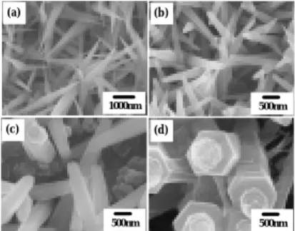
Fig. 1 (a) Low magnification SEM image showing the uniformity of the vertical aligned chromium carbide capped carbon nanotips. (b) SEM image of a close view.
Fig. 2 TEM images showing (a) the cross-section view of chromium carbide capped carbon nanotips and, (b) high magnification view of an individual carbon nanotip and the inset shows the chromium carbide head.
Fig. 3 Schematic diagram of proposed growth model (a) Formation of nucleation process; (b) cap growth; (c) deposition of carbon (d) asparagus-like structure forms.
Fig. 4 Chromium carbide capped carbon nanotip grew under bias of -300 volt for 30 minutes
Chromium can be used as a catalyst to grow chromium carbide capped carbon nanotip with size of several tens of nanometers. Surface diffusion is believed to be the mechanism for the growth of carbon nanotip. The applied bias plays an important role that either assists the growth or etches the carbon away during growth. In other words, the dimension of the chromium carbide capped carbon nanotip can be controlled. And there exits length limit which is due to the fully carburization of chromium. By supplying sufficient bias, an asparagus–like structure forms.
C. Nucleation and growth of aluminum nitride nanotips using chemical vapor deposition
100nm 100nm (a) (b) (c) (d) 200nm 200nm 200nm200nm 100nm 100nm 30 35 40 45 50 Sample D Sample C Sample B Al ( 2 0 0 ) Al ( 1 1 1 ) Al N ( 1 0 1 ) Al N ( 0 0 2 ) Al N ( 1 0 0 ) x 10 x 25 In te nsi ty (a .u .) 2 θ (degree) 0.497nm 2nm [001] 0.269nm (002) 0.497nm 2nm 2nm [001] 0.269nm (002) 20nm 20nm (a) (b) 200nm 200nm (a) (d) (c) (b) 200nm 200nm 1000nm1000nm 500nm500nm (a) (b) (c) 500nm 500nm 500nm500nm (d) 200 400 600 800 1000 -5000 0 5000 10000 15000 20000 25000 30000 35000 40000
Energy Loss (eV)
N K-edge Co u n ts 1200 1400 1600 1800 2000 500 1000 1500 2000 2500 3000 3500 4000 4500 Al K-edge Co u n ts
Energy Loss (eV)
(d) (c)
20nm 20nm
(a) (b) (c)
(AlNNTs) have been fabricated on silicon (Si) substrates by simply using thermal chemical vapor deposition at temperatures of 950°C, using aluminium (Al) powders and ammonia gas. The initial growth of AlNNTs reveal that metal- silicide nanoclusters formed during early stages of growth served as the nucleation sites for the nanotips growth. Size control can be achieved by controlling the thickness of metal catalyst deposited on the silicon substrate. A stable and self-limited (001) facet often inhibits further growth of the AlNNTs grown at high temperatures. The area of the (001) facet increases with the increasing growth temperature. The structure and chemical composition of the AlNNTs were investigated by using XRD analysis, high-resolution electron microscopy, electron energy loss spectroscopy, and elemental mapping.
Fig.1. High resolution scanning electron microscope images of AlN nanotip grown for (a) 15 min, (b) 20 min, (c) 25 min, Inset shows the high magnificent of the initial growth of nanotip with crystalline nanoparticle on the base of the AlNNTs. (d) 30 min, respectively.
Fig.2. XRD spectra take from the sample B, C, and D, respectively.
Fig. 3. (a) Low magnification HRTEM image and (b) atomic resolution TEM image of the h-AlN nanotip with growth direction of [001] with [110] zone axis. Inset in (b) shows SAED image of the AlN nanotips.
Fig.4. HR-SEM images of AlN nanotips grown with (a) Au (15nm), (b) Al (15nm), (c) Pt(15nm), (d) Pt (60nm) coating on the Si substrate, respectively.
Fig.5. HR-SEM images of AlN nanotips on silicon substrates coated with 15 nm of gold grown under (a) 950 , (b) 1000 , ℃ ℃ (c) 1100 , (d) 1200 , respectively.℃ ℃
Fig. 6. EELS experiments and elemental mapping of the AlN nanotips: (a) Original TEM image; (b) Al mapping; (c) N mapping. Corresponding EELS spectra exhibiting (d) Al K-edge at 1560 eV, (e) N K-edge at 401eV. All the EELS analysis were obtained from AlN nanotip(s) prepared on 15 nm Au coated Si substrate at 950 for ℃ 30 minutes.
In summary, the growth of highly pure and high density hexagonal aluminum nitride nanotips on silicon substrates via a thermal chemical vapor deposition system has been demonstrated. The AlNNTs grow by vapour-solid mechanism and their preferred growth direction (long axis) is [001]. Composition and structures of the AlNNTs have been confirmed by XRD, HRTEM, SAED, and EELS. Optimal conditions for the growth of these nanotips are 950 growth temperature ℃
and 30 minutes growth time under flowing NH3 with Au as catalyst. The
morphology of the nanotips is determined by the size of the metal or metal silicide phase nanoparticulates formed during the initial stages of growth. It is believed that this nanotip structure have potential applications as field emission tips, and other nanoscale heterojunction devices. 計畫成果自評 本計畫成功的利用多種方法合成 各種型態的奈米材料,包括奈米碳管、 奈米矽尖錐、奈米碳尖錐及奈米氮化鋁 尖錐。 在直接利用矽晶圓的情況下,藉由 偏壓輔助微波電漿化學氣相沈積法,可 蝕刻形成矽的奈米尖錐,更可再藉由後 處理披覆類鑽薄膜以增進其場發射性 質。此法可望直接利用現有半導體製程 以製作元件。另外直接利用觸媒成長法 選擇性成長奈米碳尖錐及奈米氮化鋁 尖錐,皆具有優良的性質。並深入研究 其成長特性進而控制奈米材料的外型 及組成。 除了可以直接應用於場發射元件 上,這些一維的奈米材料因具有極高的 表面積,可應用在需高表面積反應的需 求上,例如燃料電池、氣體偵測器及生 化感測器上。除此之外,這些奈米材料 仍待更進一步的開發與應用。
子計畫三:
奈米結構氧化物光子晶體材料製程與光電特性研究(2/3)
Growth kinetics and microstructure evolution of well-aligned and patterned ZnO nanorods
on Si-based substrate in aqueous solution 計畫編號:NSC92-2216-E-009-014 執行時間:92/08/01 ~ 93/07/31 主持人:陳三元 教授 交通大學材料科學與工程學系 中文摘要 在低溫下合成單晶ZnO 奈米線的成長動 力學和微結構的發展已經研究完成。在不 同特性基版上的ZnO 奈米線會表現出不 同的成長行為和方向。在純Si 基版上,ZnO 奈米線會散亂地沿著(100)優選平面或 [0110]成長方向,排列在整個基版上。由 高解析穿透式電子顯微鏡(HRTEM)觀查 可得到,散亂的ZnO 奈米線其實是自我組 裝的兩階段式成長所得到。相對的,如在 是在ZnO film/Si 的基版上,規則排列的 ZnO 奈米線是直接從 ZnO film 上沿著 [0002]方向成長。相比散亂的 ZnO 奈米 線,規則排列的ZnO 奈米線,有大的長寬 比,可以到25 到 30。另外,有一些平面 缺陷,例如疊差(stacking faults)產生是由於 ZnO 成長單元在後期快速成長的結果。這 些結果與發現暗示著,從溶液成長的規則 排列ZnO 奈米線不是直接跟基版有關,而 是跟基版的表面的凹凸率直接相關。 Abstract
Growth kinetics and microstructure evolution of single-crystal ZnO nanorods (ZNs) synthesized in aqueous solutions at low temperatures were investigated. Depending on surface characteristics of substrate, ZNs present different growth behavior and direction. On pure Si substrate, ZNs were scattered over the entire Si substrate with a preferred orientation in the (100) plane or grown along [0110] direction.
HRTEM observation demonstrates that the
scattered ZNs present two-stage growth process with a self-assembly process of ZNs in the later growth stage. In contrast, on Si wafer with ZnO film coated, well-aligned ZNs were directly grown along [0002] direction from the ZnO film on Si. In comparison with the scattered ZNs, a larger aspect ratio (length/width) up to 25-30 was obtained for the well-aligned ZNs. In addition, some planar defects such as stacking faults were probably resulted due to faster growth of ZnO growth unit in the later growth stage. These observations and findings imply that the growth of the well-aligned ZNs from the soft solution is not related to the used substrates but strongly influenced by the surface characteristics as well as roughness of the substrate.
I. Introduction
One-dimensional (1D) nanostructures have great potential for learning the fundamental concepts of the roles of both dimensionality and size in physical properties as well as for application in nanodevices and functional materials. Other than carbon nanotubes, 1D nanostructures such as nanowires are ideal systems for investigating the dependence of electrical transport, optical and mechanical properties on size and dimensionality.[1]
Zinc oxide (ZnO) is an important electronic and photonic material because of its wide and direct band gap (∆Eg = 3.37eV)
material.[2] The strong exciton binding energy of ZnO (60meV) is much larger than that of GaN (~ 25meV), which can ensure an efficient exciton emission at room temperature.[2] Recently, highly oriented nanorod array of ZnO nanostructures have demonstrated their potential applications in manufacturing electronic and optoelectronic devices.[3-5]
Various methods including chemical, electrochemical, and physical deposition techniques have been employed to synthesize 1D ZnO nanostructures such as catalytic growth via the vapor-liquid-solid (VSL) epitaxial method[6] and metal-organic-chemical vapor deposition (MOCVD).[7-8] However, those methods are expensive and energy consuming processes since they are operated under extreme conditions. It is well conceived that preparation of ZnO via solution chemical routes provides a promising option for large-scale production of this materials. Although wet-chemical approaches have been used for large oriented arrays of ZnO nanorods on polycrystalline (or single-crystalline) substrates from aqueous solutions[9-10], it is worth noting that without suitable treatment on the substrate, highly oriented ZnO nanorods grown on a Si wafer has been rarely achieved due to the larger mismatich (~40%) between the substrate and the ZnO nanorods.
Yamabi et al. reported that without undercoats on the surface, clusters of spindle-shaped hexagonal crystallite with diameters of 0.5-1.0 um were scattered over
the surface of a silicon wafer, but highly aligned arrays of ZnO nanorods with diameters of 20-100 nm can be developed on Si substrate undercoated with Zn(Ac)2
and annealed at 500oC.[10] Recently, Choy et
al. also found that high-quality ZnO
nanorods were successfully grown on a Si wafer by a wet-chemical process at 95oC for 6 h, where the Si wafer was dip-coated with 4 nm sized ZnO nanoparticles as a buffer and seed layer prior to crystal growth.[11]
These observations reveal the importance of surface characteristics or treatment in the growth of well-oriented ZnO nanorods in aqueous solution. However, little investigation was paid attention to the growth behavior and kinetics of such ZnO nanorods, in particular to tailor their orientation onto the substrates, that can be used to control the structure morphology and optoelectronic properties.
Therefore, in this work, a simple wet-chemical method was used to study the growth kinetic of both scattered and aligned ZnO nanorods on Si by monitoring the average aspect ratio of ZnO nanorods as a function as growth time in aqueous solution. By controlling the experimental conditions, well-aligned arrays of ZnO nanorods with different aspect ratios can be obtained. Moreover, high-resolution transmission electron microscopy (HRTEM) was performed to investigate the growth mechanisms of ZnO nanorods.
II. Experimental
Zinc nitrate hexahydrate (Zn(NO3)2.6H2O)
was used as the Zinc precursors to synthesize the ZnO nanorods (ZNs). Methenamine (C6H12N4), also called
hexamethylenetetramine (HMT) is a highly water soluble, non-ionic tetradentate cyclic tertiary amine and used to comply
simultaneously with the precipitation of the divalent post-transition metal Zn2+ ions, the nucleation growth of its stable oxide form, zincite ZnO. Two kinds of substrates were also used for comparison in this study. One is Si and the other is Si coated with ZnO film. The ZnO thin films were deposited on Si substrates by rf magnetron sputtering following our previous report.[12] An equimolar (0.02M) aqueous solution of Zn(NO3)2.6H2O and HMT was prepared in a
bottle. Subsequently, substrates were placed inside the aqueous solutions and heated at ambient temperature (55-95oC) for 0.1-15 h. After that, the substrates were removed from the aqueous solutions, rinsed with distilled water, and dried at room temperature overnight.
X-ray diffractometer (M18XHF, MAC Science, Tokyo, Japan) was used to examine the crystalline phase of the synthesized compounds with a scanning rate 4° (2θ) per min over a 2θ range 20- 60°. The
morphology of the ZnO nanorods was examined by scanning electron microscopy (SEM, Hitachi model S4000). Microstructure observation was performed by transmission electron microscopy (TEM) with a Philips Tecnai 20 instrument (Holland, The Nertherlands), operated at 200 keV. A double-tilt specimen holder was used to tilt several zone-axes. High-resolution images were recorded at several exact zone-axes with Scherzer defocus at –67nm and at an electron-optical magnification of 490000 to 520000.
III. Results and discussion
3.1 Phase and morphology of ZnO nanorods grown on different substrates
Two substrates, i.e., Si and ZnO-coated Si,
were used in this work to study the growth behavior of ZnO nanorods (ZNs) in the precursor solution at different temperatures of 55-95oC for several hours. No ZNs were observed below 50oC, indicating a thermal barrier for the growth of ZNs can not be overcome. Above 95oC, ZNs can not be synthesized because the reaction temperature is near to its melting point of the aqueous solution. Figure 1 shows the SEM images of the as-synthesized ZNs grown on these two kinds of substrates at 75oC for 10 h in the 0.02M solution. As shown in Fig. 1(a), ZNs with the dimension of 7-10 µm in length and 0.5-1 µm in diameter were scattered on the Si substrate. On the other hand, high density of well-aligned ZNs with dimensions of 20-200 nm in diameter and up to several µm in length were obtained uniformly when ZNs were grown on ZnOf/Si as shown in Fig.
1(b). It seems to imply that the formation of well-aligned ZNs on a pure Si substrate is difficult because a large mismatch (~40%) exists between ZnO and Si. Based on this reason, this would retard the nucleation of ZnO on Si substrate. Consequently, it strongly reveals the importance of the substrate characterization on the growth behavior of ZNs in the aqueous solution.
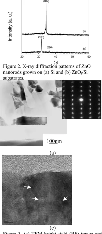
The X-ray diffraction patterns (XRD) show that the ZnO crystal phase starts to appear at 50oC and well crystallized above 65oC. As shown in Fig. 2(a) and (b), a strongly oriented peak can be indexed as the wurtzite ZnO at 75oC in 0.02 M aqueous solutions for the ZNs grown on Si and ZnOf/Si substrate. However, it should be
pointed out that a remarkable difference in XRD patterns exists between those two
substrates. As shown in Fig. 1(a), the diffraction peaks were indexed as (100), (002) and (101) planes of ZnO for the ZNs grown on Si substrate. On the other hand, Fig. 2(b) illustrates that the strongest diffraction peak corresponding to the (002) plane of ZnO was detected when the ZNs were grown on ZnOf/Si substrate. These
observations obviously imply different growth behavior between (100)-oriented (called as scattered) ZNs on Si and (002)-oriented (called as aligned) ZNs on ZnOf/Si.
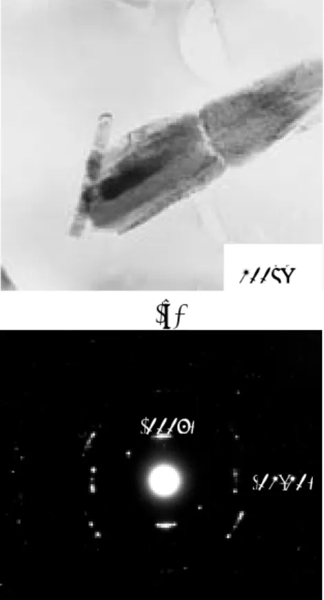
3.2. Microstructural analysis of ZnO nanorods
It is well known that ZnO has as a hexagonal lattice with c/a axial ratio of 1.602.[13] The most commonly observed morphologies of ZnO are either rod-like or needle-like crystals, especially prepared ZnO in aqueous solution because of anisotropic crystal growth. The transmission electron microscopy (TEM) bright-field (BF) image and corresponding selected-area diffraction (SAD) pattern of the scattered ZNs are shown in Fig. 3(a) and (b), respectively. The SADP in Fig. 3(b) clearly indicates that the scattered ZNs were grown along [0110] direction. This result is also
inconsistence with the XRD analysis that the ZNs are preferentially oriented along [0110]
direction. A close examination of the SADP in Fig. 3(b) shows the split of diffraction spots and extra diffraction spots, located at halfway between the central (000) spot, the {0002} spots and {0110} spots. However,
no Morié fringes were observed in the corresponding High-resolution TEM (HRTEM) in Fig. 3(c) so that double
diffraction can be neglected in this study. Since the crystallographic phase of these ZNs belongs to wurtzite structure with a space group of P63mc, it easily appears as a
characteristic “zigzag” structure,[14-15] so-called “superlattice diffraction”, corresponding to the observed extra spots in the SADP. It seems to imply that the crystal structure of the scattered ZNs was constituted from many tiny areas such as domains or mosaic texture according to the disoriented few degrees in SADP. It is well known that a crystal with mosaic structure does not have its atoms arranged on a perfectly regular lattice extending from one side of the crystal to the other; instead, the lattice is broken up into a number of tiny blocks, each slightly disoriented one from another. Within these tiny blocks, there exists a structural mismatch at the interface between these domains.[16] This mismatch may be very small and involve a difference in angular orientation between the domains as in our case with 1~2° difference in the SADP. Furthermore, HRTEM image in Fig. 3(c) recorded from this scattered ZN reveals that there seem to be two types of lattice fringes in this HRTEM image: one with wave-like fringes (as arrowed in Fig. 3(c)) and the other with straight fringes. This variation of lattice fringes as marked with arrows seems to be caused by these two types of crystal arrangements.
Figure 4(a) shows the TEM bright-field (BF) image of the aligned ZNs grown on ZnOf/Si substrate. In contrast to the
scattered ZNs, most of the ZNs were grown in a direction perpendicular to the ZnOf/Si
substrate. 4(b). A higher magnification in Fig. 4(b) indicates that the lattice fringes are
perpendicular to the longitude direction of the ZNs, and the singular fringe spacing is about 0.51nm, which is nearly consistent with the c-axis parameter in hexagonal ZnO structure (c= 0.521nm in ZnO structure). This demonstrates that [0002] direction is the preferred growth direction for the well-aligned ZNs. In addition, as one pays attention to the interface between ZNs and ZnOf/Si shown in Fig. 4(c), it was observed
that the well-aligned ZNs seem to be grown from the cup tip near the grain boundary between two ZnO grains in ZnO film. The formation of the cup shape around grain boundary between two ZnO grains is supposed to be correlated with the solution reaction during the nucleation and growth of ZNs. This demonstrates that the cup tip probably becomes a preferential nucleation position for the well-aligned ZNs grown on ZnOf/Si. However, in addition to (0002)
fringes, some ZNs with white lines dissecting the ZNs can be occasionally identified as marked with arrows in Fig. 5. This kind of planar defects can be
considered as extrinsic stacking faults with insertion of an extra Zn-O layer parallel to the basal plane. It was worth noting that the presence of (0001) stacking faults provides a possible diffusion path to modify its
optoelectronic properties according to our study. [17] However, well-aligned ZnO nanorods without any planar defects can be also obtained in aqueous solution by controlling the experimental conditions.
3.3 Growth behavior and kinetics of ZnO nanorods
It is well known that the growth behavior of ZNs was strongly influenced by the
growth conditions such as ion concentration in solutions, reaction temperature and time. As illustrated in Fig. 6, the aspect ratios (AR =length/width) of ZNs grown on Si and ZnOf/Si substrate as a function of growth
time at 75oC were measured.
When the Si substrate without ZnO film coated was placed in the Zn-containing aqueous solution, in the initial growth stage of ZNs, prior to 0.2h, no obvious ZNs can be detected. However, above that (0.2-0.3h), it can be observed that a small amount of ZNs with ~20 nm in diameter and ~60 nm in length were randomly scattered on Si substrate according to SEM images (not shown here). However, at the same period of growth time, no any well-aligned ZNs can be clearly observed from the Si substrate. It seems to imply that the formation of well-aligned ZNs on a Si substrate is difficult based on the lattice parameters of ZnO and Si because a large mismatch (~40%) exists between ZnO and Si and this would retard the nucleation of ZnO on Si substrate. This phenomenon reveals that the well-aligned ZNs remain in the nucleation stage, but the scattered ZNs are going through nucleation and growth stage. Until 0.5 h, the well-aligned ZNs can be clearly obtained but the scattered ZNs have been grown with an AR of 2-3. Subsequently, with an increase of growth time, it can be observed that the increasing rate of the AR becomes slower in the scattered ZNs as compared to that in the well-aligned ZNs. Especially, above 5 h, the AR for the scattered ZNs remain unchanged with a constant of about 9-11 but the AR is also slightly decreased with increasing growth time up to 15 h. This implies that the
scattered ZNs did not further grow as expected despite extending growth time. As evidenced from the TEM BF image and corresponding SADP of ZNs grown for 5 h in Fig. 7, it seems to indicate that more than two ZNs with the same [0110] growth
direction were self-assembled together to form a bundle. The TEM dark-field (DF) image clearly reveals that more than two ZNs were aggregated in a coplanar manner using their side planes to form a large ZN as shown in Fig. 7(c). This bundle ZNs can be further transformed into another ZN with a larger dimension in diameter. In other words, the side crystal planes of the ZNs were able to glue together to form a larger crystal. This behavior is also called “oriented attachment”.[18] Based on viewpoint of thermodynamic, this self-assembling process is possible for the synthesized ZNs to reduce total Gibbs free energy in the later growth stage. This phenomenon is very similar to the Ostwald ripening occurring in ceramic sintering progress. This observation may be used to explain the slight decrease in AR in the later growth stage (5 -15 h). Consequently, the growth behavior of the scattered ZNs can be considered as a two-step growth mechanism.
In contrast, as the ZnOf/Si substrate was
used and immersed into the precursor solution for the growth of ZNs, it was found that in the early stage (t < 0.5), no aligned ZNs can not be clearly observed from the ZnOf/Si substrates but at t = 1 h, a smaller
AR was obtained for the well-aligned ZNs compared to that of scattered ZNs. It was believed that the ZnO nuclei will be preferentially grown on the ZnOf/Si
substrate in this stage and the promotion of
heterogeneous nucleation is ascribed to the high affinity of the nuclei of ZnO for the surface, especially formed at the cup sites as shown in Fig. 4(c). In this condition, although an inherent asymmetry along the c axis allows the anisotropic growth of the crystal along the [0002] direction, the lateral growth along different directions are possible for the nucleus to decrease the roughness of the film surface because of surface energy effect. When the favorable nucleation position of ZN was formed on the ZnO film, ZnO growth unit (or called coordination polyhedron) will stack in order and grow along [0002] direction. Subsequently, a fast growth along longitudinal direction (c-axis) for the well-aligned ZNs was expected because the growth in width direction is suppressed due to the size of cup shape in ZnOf/Si substrate.
In 15 h, well-aligned and highly oriented ZNs with an aspect ratio up to 25-30 can be obtained. These results can be used to explain the observation that the well-aligned ZNs with a smaller AR were formed in an early stage but later, the ZNs were rapidly grown along the longitudinal direction in the later growth stage. Therefore, in this condition, some stacking faults are accidentally observed as shown in Fig. 5 that is probably due to faster stacking and the instability of the polar (002) plane in ZnO.
3.4
Figure 1a shows the surface images of large-scale arrayed ZnO nanorods grown on polystyrene (PS)/polycarbonate (PC) substrates. It was found that the ZnO nanorods have a well-defined hexagonal plane with a homogeneous diameter of
approximately ~60 nm due to uniform growth rate. The cross-section image in Figure 1b shows that the ZnO nanorods with a uniform length of 1.5 µm are directionally and densely grown over the entire PS surface of the substrates. Furthermore, we found that the patterned ZnO nanorods (Fig. 1c) can be developed after the removal of the PS beads in the specimen produced by the same conditions as Fig 1b. It implies that the PS layers can act as a nucleation base to supply the appropriate environment to increase the probability of the high density of nucleation sites and enhance the crystal growth.
To understand how the well-aligned arrays of oriented ZnO nanorods were formed on the organic substrates, the sample was further investigated by SEM and TEM. Three stages can be identified for the growth of ZnO nanorods on PS layers. The first initial stage (t < 0.5 h) is the induction time, during which an ultra-thin monolayer was slowly generated under the surface of PS beads in the solution. It is difficultly observed by SEM microscopy but the ultra-thin monolayer can be simply detected to be ZnO signal by chemical analysis such as X-ray photon spectroscopy (not shown) after removing the PS beads. The second stage is the nucleation period, during which the concentration of the building units in the solution builds up until a critical super-saturation level is reached and then nucleation occurs (Fig. 2a). It was believed that the ZnO nuclei will be preferentially grown on the concave regions of PS layers in this stage and the promotion of heterogeneous nucleation is ascribed to the high affinity of the ZnO nuclei to the PS
surface. After nucleation, in the third period, a fast growth along longitudinal direction (c-axis) for the oriented ZnO nanorods was expected because the growth in width direction is suppressed due to the size of concave shape in PS layers as shown in Fig. 2b. Figure 2c shows the high resolution TEM (HRTEM) image of the well-aligned ZnO nanorods grown on PS/PC substrates. It indicates that the lattice fringes are perpendicular to the longitude direction of the ZnO nanorods, and the singular fringe spacing is about 0.51nm, which is nearly consistent with the c-axis parameter in hexagonal ZnO structure (c= 0.521nm in Wurtzite ZnO). This demonstrates that <001> direction is the preferred growth direction for the well-aligned ZnO nanorods. Recently, it was reported the aligned ZnO nanorods can be grown on the Si substrates with ZnO buffered layers which consists of nanoparticles or crystalline films.16,17 However, most reports in the literature ignored the effect of surface morphology on the nucleation base of the aligned ZnO nanorods. Therefore, a HRTEM analysis was paid attention to the interface between ZnO nanorods and ZnO monolayer (~5 nm thicker) shown in Fig. 2d after removing the PS beads. It was observed that the well-aligned ZnO nanorods seem to be grown from the concave tip near the grain boundary between two ZnO grains in ZnO monolayer. A detail investigation for the growth behavior and kinetics of ZnO nanorods grown on inorganic substrates were reported in our previous study.19 This demonstrates that the well-aligned ZnO nanorods can be grown on organic and inorganic substrates with controlled surface
morphology.
Figure 3a presents the SEM surface image of ZnO nanorods grown on organic substrates more than 24h. It was found that the ZnO nanorods begin to amalgamate with other neighboring nanorods and their growth becomes physically limited. In comparison with Fig. 1a, the ZnO rods become much thicker (more than 0.5 µm) but not much longer (about 1.7 µm) after long-term growth because the ZnO nanorods have started on coalescence process with adjacent rods. Therefore, after the lateral growth begins, the growth rate of ZnO nanorods in the <001> orientation would obviously decrease. The TEM bright-field (BF) image (inset in Figure 3a) of the <001> zone-axis of (cross-sectional) ZnO nanorods clearly illustrated the merged grains with side crystal plane attached. Moreover, as confirmed by Figure 3b for the <001> zone-axis selected-area electron diffraction (SAED) pattern of ZnO nanorods. The split diffraction spots in the edge region (marked with arrows) of the SAED pattern suggest that the merged ZnO nanords are not perfectly aligned in both a and b directions. The longitudinal direction is along the c <001> orientation. The TEM images in Fig. 3c and d reveal the BF and dark-field (DF) images of the merged ZnO nanorods, respectively. The DF image in Fig. 3d clearly and visibly shows that more than two ZnO nanorods were aggregated in a coplanar manner using their side planes to form a larger ZnO nanorod. A magnified picture of Fig. 3c was illustrated in Fig. 3e. The insets in the left and right of Figure 3e present the SAED patterns of single and couple nanorods in coalescent ZnO nanorods,
respectively. The split diffraction spots were also identified from the couple rods and a slight misalignment between nanorods was observed. The growth behavior of the larger ZnO nanorods in later long-term growth can be considered from direct combination of a small number of individual nanorods which was similar to oriented attachment.2
IV. Conclusion
We have developed a low-temperature synthetic route to prepare well-aligned arrays of oriented ZnO nanorods with high crystallinity in the diameter of ~60 nm on the Si substrates. Single-crystal ZnO nanorods (ZNs) can be synthesized in an aqueous solution at 75oC. Depending on the surface characteristics of the substrate, ZNs present different growth behavior and direction. On pure Si substrate, ZNs were scattered over the entire Si substrate with a preferred orientation in the (100) plane or grown along [011 0] direction. HRTEM
observation demonstrates that the scattered ZNs present two-stage growth process with a self-assembly process of ZNs in the later growth stage. In contrast, on Si wafer with ZnO film coated, well-aligned ZNs were directly grown along [0002] direction from the ZnO film on Si. In comparison with the AR of the scattered ZNs, a larger AR up to 25-30 was obtained. Although the surface characteristics of the substrates plays a very important role in both scattered and well-aligned growth of the ZNs, the ZnO film on Si wafer is surely to reduce the mismatch between the Si substrate and the ZnO nanorods. This simple approach should promise us a future large-scale synthesis of the patterned growth of the highly
well-aligned ZNs on various kinds of substrates buffered with a controlled morphology and roughness layer in an aqueous solution at low temperatures.
Acknowledgments
This work was financially supported by the National Science Council of the Republic of China, Taiwan under Contract No. NSC-92-2216-E-009-014.
References
(1) Hu, J.; Odom, T. W.; Lieber, C. M. Acc.
Chem. Res. 1999, 32, 435.
(2) Zamfirescu, M.; Kavokin, A.; Gil, B.; Malpuech, G.; Kaliteevski, M. Phys. Rev.
B. 2002, 65, 161205.
(3) Lieber, C. M.; Cui, Y. Science 2001, 291, 851.
(4) Duan, X.; Huang, Y.; Cui, Y.; Wang, J.; Lieber, C. M. Nature 2001, 409, 66.
(5) Park, W. I.; Yi, G.; Kim, M.; Pennycook, S. J. Adv. Mater. 2003, 15, 526.
(6) Wu, Y.; Yang, P. J. Am. Chem. Soc. 2001, 123, 3156.
(7) Chiou, W. T.; Wu, W. Y.; Ting, J. M.
Diam. Relat. Mater. 2003, 12[10-11], 1841.
(8) Lee, C. J.; Lee, T. J.; Lyu, S. C.; Zhang, Y.; Ruh, H.; Lee, H. J. Appl. Phys. Lett. 2002, 19, 3648.
(9) Vayssieres, L.; Keis, K. J. Phys. Chem.
B 2001, 105, 3350-3352
(10) Yamabi, S.; Imai, H. J. Mater. Chem. 2002, 12, 3773
(11) Choy, J. H.; Jang, E. S. Adv. Mater. 2003, 15, 1911
(12) Lin, C. C.; Hsiao, C. S.; Chen, S. Y.; Cheng, S. Y. J. Electrochem. Soc. 2004, in press.
(13) Bailar, J. C.; Emeleus, H. J.; Nyholm, R. and Trotman-Dickenson, A. F. Comprehensive inorganic chemistry,
vol. 3. Pergamon Press, Oxford, 1975. (14) Manna, L.; Scher, E. C.; Alivisatos, A.
P. J. Am. Chem. Soc. 2000, 122, 12700.
(15) Trentler, T. J; Hickman, K. M.; Goel, S. C.; Viano, A. M.; Gibbson, P. C.; Buhro, W. E. Science 1995, 270, 1791.
(16) A. R. West, Basic solid state chemistry, pp. 244, John Wiley & Sons, 1999.
(17) C. C. Lin, H. P. Chen and S. Y. Chen, submitted to Adv. Mater. (2004). (18) Liu, B.; Zeng, H. C. J. Am. Chem. Soc. 2003, 125, 4430
(a)
(b)
Fig. 1. SEM micrographs of ZnO nanorods
grown on different substrates: (a) Si substrate and (b) ZnOf/Si substrate.
10um
20 30 40 50 60 (010) (100) (002) (a) (b) In tens it y (a. u. ) 2θ 50nm
Figure 2. X-ray diffraction patterns of ZnO
nanorods grown on (a) Si and (b) ZnOf/Si
substrates.
(a)
(c)
Figure 3. (a) TEM bright field (BF) image and (b) corresponding selected area diffraction pattern of ZnO nanorods grown on Si substrate. (c) Showing the lattice fringes of ZnO nanorods in (a).
(a)
(b)
(c)
Figure 4 (a) TEM bright field (BF) image of
aligned ZnO nanorods (ZNs) grown on ZnOf/Si
substrate. (b) High-resolution TEM images of the aligned ZNs and (c) the interface region
between ZNs and ZnOf/Si.
100nm
5nm
Figure 5. High-resolution TEM (HRTEM) image of ZnO nanorods showing the presence of stacking faults (SFs) as marked with arrows.
Figure 6. Dependence of aspect ratio (AR) on growth time for scattered and aligned ZnO nanorods.
(a)
(c)
Figure 7. (a) TEM bright-field image, (b) corresponding selected area diffraction pattern and (c) dark-field image of self-assembled ZnO bundles.
Figure 8. SEM images of large arrays of oriented ZnO nanorods grown on polystyrene (PS)/polycarbonate (PC) substrates for 8 h. (a) Low magnification, face-on view. (b) Cross-sectional SEM image of ZnO nanorods grown PS/PC substrates. (c) SEM image of ZnO nano.
Figure 9. SEM images of ZnO nanorods grown on PS/PC substrates as a function of reaction time at 75 ℃ . (a) 1h, and (b) 5 h. (c) High-resolution TEM image of ZnO nanorods grown on organic substrates. (e) High-resolution
100nm
(0002)
TEM image of the interface region between ZnO nanorods and ultra-thin ZnO monolayer/PC.
Figure 10. (a) Face-on view SEM image of well-aligned ZnO nanorods grown on PS/PC substrates for long-term growth (>24h). A <001> zone-axis TEM bright-field(BF) image of the coalescent ZnO nanorods (its scale bare is 100nm in the insert), and (b) a corresponding diffraction pattern for the inser of Fig. 3a. (c) Cross-sectional TEM (BF) and (d) dark-field (DF) images of the coalescent ZnO nanorods. (e) A high magnification BF TEM image of (c), showing the interface ( marked with dash line) of the coalescent couple ZnO nanorods.
子計畫四:磊晶氧化鋅之製程及特性研究(2/3)
計畫主持人: 張 立
計畫編號: 92-2216-E-009-011-
參與人員: 林智偉、吳佳玲
本年度計畫進行CVD 鍍膜研究,化學氣相沉積系統(CVD)腔體內固定,量 取適當前驅物Zn(C5H7O2)2於氧化鋁坩堝內並放置系統中。在成長過程中,Si 基 板溫度為500℃,腔體壓力為一大氣壓。通入氮氣作為攜帶前驅物的氣體,前驅 物的加熱溫度控制在134℃。通入氧氣於腔體中進行反應,氧氣加熱溫度為 500℃。氮氣和氧氣流量均為 500ml/min。其中一部分在 Au/Si 基材上鍍具有高 指向之ZnO 膜,另外一部分在 Y2O3/Si(111)基材鍍上磊晶 ZnO,分別敘述如下。一、在Au/Si 基材上鍍具有高指向之 ZnO膜 試片成長時間分別為60 分鐘(試 片A)與 120 分鐘(試片 B)。XRD、SEM 與TEM 結果顯示成長之氧化鋅結構具 有良好的(0002)優選方向之柱狀結構 二、Y2O3/Si(111)基材 使用CVD 和 PLD 方法鍍 ZnO 薄膜於 PLD 成長之 Y2O3/Si 基板上。穿透式電 子顯微鏡(TEM) X 光繞射得知兩者方 法成長的ZnO 品質很接近,街有磊晶 之現象。 兩者都顯示出ZnO 與 Y2O3之間的晶體 方 向 關 係(orientation relationship) 為 {0002}ZnO//{111}Y2O3 , <0110>ZnO//<112>Y2O3 , {11 2 0}ZnO//{440}Y2O3 。
子計畫五:
用晶圓接合與溼式蝕刻方式來剝離側向覆蓋生長之氮化鎵磊晶層
(2/3)
一、摘要 1. 中文摘要 關鍵詞:氮化鎵,晶圓接合, 異質磊晶,藍寶石,側向覆蓋 生長。 本計畫主要的目的在於解決 氮化鎵(GaN)薄膜異質磊晶 (heteroepitaxial)於藍寶石 (sapphire)基材所衍生的許 多問題。期望藉由晶圓接合 (wafer bonding)搭配濕式蝕刻 (wet etching)於側向覆蓋生長 磊晶片(ELOG GaN)上,轉移 氮化鎵磊晶層於它種基板上。 在前一年(第一年)的計畫 中,我們發現由於在ELOG GaN 上之遮罩層(mask)僅剩 300-500 埃(Å),蝕刻液很 難有效的移除晶圓接合後的 遮罩層。在這一年(第二年) 的計畫中,我們先將ELOG 上之遮罩層蝕刻後,在與晶圓 接合,然後再移除藍寶石基 材。此外,長在GaAs 基板的 AlGaInP LED 結構,也被用 來模擬轉移到Cu 基板之效 果。 2. 英文摘要 Keywords:gallium nitride, sapphire, wafer bonding, heteroepitaxial, mask layer, epitaxial lateral overgrowth, epitaxy layer transfer.This project was designed to solve the heteroepitaxial growth of GaN on the sapphire substrate. By selective wet etching of mask of the epitaxial lateral overgrowth (ELOG) GaN and bonding with other handle wafers, the ELOG GaN layers were transferred to handle wafers. 二 、前言及研究目的 氮 化 鎵 具 有 優 越 的 光 電 特 性,且當其與氮化鋁(AlN)、氮 化銦(InN)等化合物混合生長時 可 使 能 階 由 2.0ev 連 續 改 變 至 6.3ev。幾乎涵蓋了所有可見光的 範圍,造成近年產官學界均投入 大量的資源進行相關的研究。然 而,受限於熱力學需高溫高壓生 長的先天限制,截至目前,大尺 寸品質良好的氮化鎵塊材晶體, 尚很難取得。因此目前商業用途 的氮化鎵材料都是經由氣相沈積 (vapor phase deposition)於非氮 化鎵之氧化鋁基板上。但藍寶石 本身的材料特性也使得氮化鎵材 料的應用發展受到了限制,例如: 1. 藍寶石導熱性質不佳,元件容易 產生Joule heating 的效應,這不僅 使元件效能變差,更使得元件的 壽命與與可靠性減低。 2. 藍寶石本身是不導電的材料,使 得兩電極之結構均必須鍍於元件 作用層之上方。也正因基板不導 電造成此元件之特殊結構,使得
製作氮化鎵發光二極體的過程必 須多一道微影蝕刻的步驟,將氮 化鎵磊晶層表面之部份 P 型區域 去除,露出 N 型氮化鎵磊晶層, 如此才可以於同一面同時獲得 P 型與 N 型氮化鎵之半導體表面。 但由於氮化鎵具備半導體材料當 中鍵結最強的離子性,相對於傳 統的三五族半導體材料對於蝕刻 液顯得較為鈍態,因此必須使用 乾 式 的 方 式 ( 如 ECR-RIE 與 ICP-RIE)進行氮化鎵的蝕刻製 程,但使用乾式蝕刻氮化鎵還有 光阻去除不易以及易損傷磊晶層 品質等問題,進而影響元件的量 產品質。由此可知,氮化鎵的不 導電基板不僅增加元件製程複雜 度並使得製造良率下降,還必須 犧牲部分 發光 的作用 層(active layer)供 N 型電極所用,降低了 元件單位面積的發光亮度。 3. 製作氮化鎵發光二極體時,藍寶 石基材必須有一定厚度(一般> 300μm)以避免因高溫而產生的 變形。但因藍寶石的硬度過高(其 莫氏硬度為9),使得元件製作完 成後不易進行dicing,又因為藍寶 石晶體對稱性的影響,造成使用 傳統 dicing saw 的切割方式會損 失較大面積的磊晶層,且切割刀 具的磨損量也會增加並導致生產 成本增加。切割過程中的藍寶石 不規則崩裂也使我們無法得到想 要的晶粒形狀,造成生產良率降 低。 4. 由於藍寶石與氮化鎵晶格常數的 不 匹 配 和 熱 膨 脹 係 數 的 差 異 極 大,導致磊晶生長時氮化鎵薄膜 的缺陷如差排、疊差等等…密度 甚高。在藍寶石與氮化鎵界面處 的差排(dislocation)密度常高達 1010cm-2以上,並且會延伸到元件 結構之上。磊晶缺陷的存在容易 使作用層失效並大幅的降低元件 的特性。 透過晶圓接合技術,則可 以將氮化鎵薄膜轉移到導電 性和導熱性較佳的其他材料 基板上。 本實驗室在在第一年的 計畫中,發現由於在ELOG GaN 上之遮罩層(mask)僅剩 300-500Å(原本為 1000Å), 蝕刻液很難有效的移除晶圓 接合後的遮罩層。在這一年的 計畫中,利用長出未密合的 ELOG 的 GaN,將 ELOG 上 之遮罩層蝕刻後,在與晶圓接 合,然後再移除藍寶石基材。 此外,長在GaAs 基板的 AlGaInP LED 結構,也被用 來模擬轉移到Cu 基板之效 果。 三 、研究方法 在氮化鎵側向覆蓋成長 法當中,會鍍覆數百至1,000Å 的SiO2遮罩層(mask) 。經由 一般的IC 蝕刻方式,蝕刻出 條狀的遮罩層。在經由氣相沈 積出未密合的ELOG GaN。以 上部分,是由廠商製造。我們 將ELOG 上之遮罩層蝕刻 後,在與晶圓接合,然後再移 除藍寶石基材。 由於現階段所得之 ELOG GaN 非發光的 LED 結 構。為證明晶圓接合及轉移基 板之效果。所以我們拿,長在 GaAs 基板的 AlGaInP LED 結構,轉移到Cu 基板,來作 模擬。其中, ITO 層被拿來 當作current-spreading 與中 間接合介質。經過在無塵室清 洗後,放在Ar 氣氛中,在
400°C 至 600°C 接合 30 分 鐘。 三 、結果與討論 1. ELO GaN 之晶圓接合及分離 在SiOx的遮罩層移去 後,ELO GaN 與 Cu 基板在 500 ~ 600°C 進行接合。冷卻 後,於Sapphire 基板上易有 crack 產生,如圖(一)所示。 其原因可能是在冷卻時, Sapphire 與 Cu 之熱膨脹係數 之差異(Sapphire= 7.5×10⁻⁶/K﹔Cu = 16.8× 10⁻⁶/K) 而產生熱應力。施予 適當之剪應力,可將基板分 開。若先以淬火之方式增加薄 膜間的應力,再加上適當之剪 應力,可得到較佳之分離效 果,如圖(二)所示。 最後,為了判斷bonding 對薄膜之特性是否有影響,藉 由 PL 光譜圖發現 bonding 前 後之FWHM 並無改變,但 bonding 後之試片有 blue shift 的現象產生,其原因可能為於 氮化鎵結接合於銅基板,因降 溫時氮化鎵薄膜之熱膨脹係 數分別小於銅與藍寶石基 板,而產生壓縮應力所致。 2. AlGaInP LED 結構轉移到 Cu 基板 我們發現,當溫度低於400℃ 時,樣品無法接合,溫度若高 到600℃的話,銅又會滲透 ITO 層,導致 LED 的結構遭 到破壞。在500℃下加熱 30 分鐘,銅尚不會穿透ITO 層, 而樣品又可以順利接合。轉移 後的試片如圖(三)所示。由 於銅具有較高的熱導率及較 低的熱阻抗,因此散熱的效果 較佳。如圖(四)所示,比起 傳統的GaAs 基板的 LED,銅 基板LED 的操作電流可以高 達800 mA,而其發光峰值強 度可高達1230 mcd。該系統 於室溫下連續以20 mA 的電 流操作500 個小時後,其發光 強度衰減的幅度不到5%。詳 見我們在Applied Physics Letters 發表之論文。[1] 三 、未來的方向 (1) 請 合 作 的 單 位 廠 商 提 供 LED 或 LD 結構之 ELO GaN。 (2) Cu 基板之切割。
(3) 不同之導電/導熱基板,以 利試片之切割。
四 、參考文獻
1. Wei Chih Peng and YewChung Sermon Wu, " High-power AlGaInP light-emitting diodes with metal substrates fabricated by wafer bonding," Appl. Phys. Lett. 84(2004) PP1841-1843.
圖一 氮化鎵接合於銅基板上,冷卻後, Sapphire 基板上有 crack 產生。
(a) GaAs Substrate LED (b) Cu Substrate LED 0 200 400 600 800 1000 1200 1400 0 200 400 600 800 1000 LUMINANCE INTE NS ITY (mcd) CURRENT (mA) 圖二 以淬火之方式再施予適當之剪應 力之試片。 圖三 LED 接合在 Cu 基板上之(a)上視圖 (b)剖面圖。
圖四 (a) GaAs Substrate LED 與(c) Cu Substrate LED 之 L-I 曲線
200µm
(a)
(b)
LED epi
子計畫六:
光記錄媒體材料、性質及其應用於光碟記錄容量提升之研究(2/3)
A Study of Optical Recording Media, Properties and Their Applications
to Increase the Storage Capacity of Optical Disks (2/3)
計畫編號:NSC92-2216-E009-013
執行期限:92/08/01 – 93/07/31
主持人:謝宗雍 國立交通大學 材料科學與工程學系 教授
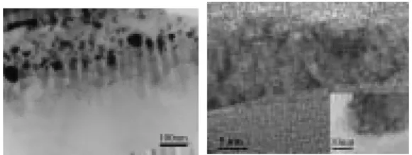
一、 中文摘要 本年度之研究包含(1)GeInSbTe(GIST) 光碟資料傳輸速度之提升與(2)ZnO-SiO2微 晶玻璃(Semiconductor-doped Glass,SDG)材料 之開發。在光碟資料傳輸速度之提升部分,氮 氣摻雜被應用於提昇非晶相-晶相的相變化速 度。以氮氣摻雜來產生許多均勻分佈於記錄層 的微小氮化物,而這些氮化物的存在則提供許 多有利於非晶相-晶相間相變化的優選位子。 當摻雜的氮氣/氬氣比率為 3%時,GeInSbTe 相變化記錄光碟在無嚴重損害訊號抖動(Jitter) 值的情況下,其再結晶速率增加約1.6 倍。微 晶玻璃(SDG)部分,本計畫以貼靶濺鍍法在 SiO2中長成5 至 10 nm 奈米分佈之 ZnO 微粒, PL 量測顯示貼靶面積增加至 20%、30%時, 發光峰值約為560 至 580 nm,符合 ZnO 的綠 光轉換特性(Green Band Transition),此能階主 要為 ZnO 自身缺陷所形成;當低貼靶面積時 的發光峰值則偏移至470 nm。造成 ZnO 量子 點的光譜峰值向短波長呈現不連續偏移的原 因尚未明瞭,有待後續之研究探討 ZnO 量子 點的量子侷限效應(Quantum Confinement)與 結構缺陷對發光特性的影響。 關鍵詞:GeInSbTe 光碟、資料傳輸速度、 ZnO-SiO2微晶玻璃。Abstract:This project of this year studies the enhancement of data transfer rate of GeInSbTe optical disk and the preparation of ZnO-SiO2 SDG thin film. Nitrogen doping was applied to enhance the velocity of amorphous-crystalline phase transformation. The N2 doping produced tiny nitride precipitates uniformly distributed in the recording layer and provided numerous preferential sites for phase transition. At the doping N2/Ar ratio = 3%, the recrystallization velocity of GIST phase change recording media was increased up to 1.6 times without severely damaging the signal jitter values. In the part related to ZnO-SiO2 SDG films, the emission
peak measured by PL was about 560 ~ 580 nm (yellow) with the chip area coverage ratio of 20% and 30%. The emission was caused by the recombination of the carrier at the deep trap levels that are induced by the intrinsic defects of ZnO. However, the emission peak shifted to about 470 nm (blue) with low chip area ratio. The reason causing the un-continuous shift of the emission peak to shorter wavelength is unclear and future study is required.
Keyword: GeInSbTe optical disk, data transfer
rate, ZnO-SiO2 SDG thin film. 二、緣由與目的 數據資料之儲存與取用是當今資訊產品 使用中的重要部份。現行資料之儲存可分為磁 記錄與光記錄兩大類,光記錄通常以雷射光進 行資料之記錄,是當今資料儲存最熱門、最重 要的產品。 光碟研究的重要方向之一為提高資料傳 輸速率,故相變化光記錄材料必須擁有更高的 非晶相-晶相相變化速度。共晶系統的銻-碲 (Sb-Te)合金亦或稱為快速成長型相變化合金 最為大家所注目,因為此材料在短波長雷射及 高數值孔徑的透鏡系統下擁有良好的訊號特 性及較高的再結晶速率。本實驗以氮氣摻雜於 相變化光碟的GeInSbTe 記錄層中,並以動態 測試機對其訊號特性及資料傳輸速率加以研 究,而穿透式電子顯微鏡(TEM)則是被用來觀 察氮氣摻雜對微結構所造成的影響,並且更進 一步對微結構的變化與再結晶速率(或資料傳 輸速率)做探討。 光碟的另一重要研究方向為提升紀錄密 度,使用短波長、藍光雷射的讀寫頭為改善之 方法之一[1]。目前所量產的藍光 LED 主要以 GaN 做為活性發光區,然而由於 GaN 缺乏良 好晶格匹配的基板,加上氮化物的強化學穩定 性使得微影蝕刻製程需以 RIE 進行,在形成 Ti/Al 歐姆接觸時容易形成 TiN 或 Al2O3而造 成電阻值的增加,加上 p-GaN 成長不易,因