國 立 交 通 大 學
電子工程學系 電子研究所碩士班
碩 士 論 文
利用二段式熱化學氣相沉積法成長不同間距
高度比之奈米碳管柱列之場發射特性研究
Study on the Improvement of the Field Emission
Characteristics of Carbon Nanotube Pillar Arrays with
Different Pitch/Height Ratios Using Two-Step Thermal
Chemical Vapor Deposition
研 究 生: 魏 英 彰
指導教授: 邱 碧 秀 博士
鄭 晃 忠 博士
利用二段式熱化學氣相沉積法成長不同間距
高度比之奈米碳管柱列之場發射特性研究
The study of Study on the Improvement of the Field Emission
Characteristics of Carbon Nanotube Pillar Arrays with Different
Pitch/Height Ratios Using Two-Step Thermal Chemical Vapor
Deposition
研 究 生:魏英彰 Student:Yin-Chang Wei
指導教授:邱碧秀 博士 Advisor:Dr.
Bi-Shiou Chiou
鄭晃忠 博士 Advisor:Dr. Huang-Chung Cheng
國 立 交 通 大 學
電子工程學系 電子研究所碩士班
碩 士 論 文
A Thesis
Submitted to Department of Electronics Engineering & Institute of Electronics College of Electrical Engineering and Computer Engineering
National Chiao Tung University In Partial Fulfillment of the Requirements
For the Degree of Master In Electronics Engineering July 2009 Hsinchu, Taiwan
中華民國九十八年七月
利用二段式熱化學氣相沉積法成長不同間距
高度比之奈米碳管柱列之場發射特性研究
學生:魏英彰 指導教授:邱碧秀 博士
鄭晃忠 博士
國立交通大學
電子工程學系 電子研究所碩士班
摘 要
此篇論文之實驗當中,成長奈米碳管方面,為了可以減低成本且能夠均勻的將奈米 碳管應用於場發射顯示器當中,熱化學氣相沉積法比起其他分法具有簡單且低成本的優 勢,因此被認為是最具有潛力的碳管成長發法之一。在催化金屬的使用方面,於多層共鍍 催化金屬合成柱狀形式奈米管的奈米探管陣列於場發射的應用,採取了鈷鈦共鍍的合金, 此方式不僅得到高度一制性的碳管管徑並且利用了金屬鈦於高溫下與炭的化合結果,能 夠有效提升奈米碳管對於基板的附著能力以及展現較佳的場發射特性。 首先,根據以往關於柱狀形式奈米碳管用於場發射方面的論文當中,數種不同高寬 比都被提及,例如 R/H = 6,R/H=3,R/H=2 等,並沒有真正探討出高寬比與柱狀形式奈 米碳管陣列組合上之絕對關係,在這實驗當中,設計了三種不同柱狀奈米碳管之間的間 距,且由控制成長時通入碳源的流量與成長的時間可以穩定成長出所需要柱狀奈米碳管 的高度,進而討論其 R/H 值,當中,也發現到當柱狀奈米碳管之間的間距越遠,可以得 到其對應最小起始電場的理想 R/H 值有趨近於 2 的趨勢,實驗中定義了電流密度為 J=10
μA/cm2 對應到的電場為起始電場,在間距 80μm,150μm 與 250μm 最佳 R/H 值為 8, 4.7 與 3.2 分別能夠對應到最小起始電場為 Eturn-on=1.78V/μm, Eturn-on=1.55V/μm 與 Eturn-on=1.53V/μm,並且在最佳 R/H 情況下可以得到均勻性最佳的場發射效果。 根據先前實驗中奈米碳管成長機制,倘若要得到長度較長的奈米碳管,必須控制其成 長時碳源氣體流量與成長時間的搭配,因此,改良了單一階段成長的參數而成功的達到 二階段形式的成長方式,此方法不僅能夠成長出較高的柱狀碳管並且在場發射方面可以 得到相當優異的起始電場 Eturn-on=0.1V/μm,以及飽和電場 Ethreshold=0.3 V/μm,實驗中也定 義了電流密度為 J=10mA/cm2
對應到的電場為飽和電場,並且利用了 SEM, Raman, TEM 作 了材料特性方面上的分析。 由於奈米碳管密度會影響其場發射特性,為了使其均勻特性有效提升,近一步使用電 漿來改善柱狀奈米碳管的表面密度分佈是可行的方法之一,本論文中提出了使用純氧電 漿或氧氣加氯氣的電漿作為柱狀奈米碳管的後段處理,當中發現氧氣加上氯氣的電漿可 以藉由改變轟擊的時間,造成某些奈米碳管被摧毀,而留下一些較高的奈米碳管,而這 些較高的奈米碳管表現了較高的場發射電流,當中也明顯發現了,經過電將處理後柱狀 奈米碳管的幾何型態有顯著的變化,也因為型態上的改變使得電場遮蔽效應的下降,以 致於起始電場的降低與均勻性顯著的提升,並且得到了當氧氣加氯氣電漿處理三分鐘後 的結果,電場遮蔽效應能夠最有效的抑至,而起始電場 Eturn-on=1.4V/μm 相較於未經過電 漿後處理的起始電場 Eturn-on=2.6V/μm 有很明顯的下降。 最後,在奈米碳管場發射的應用當中,低操作電壓是個很重要的因素,因此設計了 一種溝槽式的奈米碳管三極結構,利用氧化層來取代傳統的絕緣間隙層,藉由控制奈米 碳管的長度可以改變閘極到發射極的間距,實驗中固定陽極電壓為 800V,當閘極電壓從 0V 增加到 80V 時,場發射結果的亮度和均勻性都會大幅提升,並且論文中也利用了 SIMION 3D 軟體,模擬了不同閘極到發射極的間距與閘極對於均勻性的影響,因此這結構 應用於奈米碳管場發射將是不錯的優勢。
Study on the Improvement of the Field Emission Characteristics
of Carbon Nanotube Pillar Arrays with Different Pitch/Height
Ratios Using Two-Step Thermal Chemical Vapor Deposition
Student: Yin-Chang Wei Advisor: Dr. Bi-shiou Chiou
Department of Electronics Engineering & Institute of Electronics
National Chiao Tung University
Abstract
Cost reduction and uniformly distribution of carbon nanotubes are the two main topics in the field emission display application. Thermal chemical vapor deposition (T-CVD) is regarded as one of the best candidates of the growth methods due to the merits of simplicity and cost efficiency in the fabrication and large scalability. Besides, we also find titanium (Ti) layer can improve the uniformity and strengthen the adherence between the CNTs and substrate for CNTs’ growth. Therefore, co-deposited multilayer catalyst composed of Co and
Ti on Al (Co-Ti/Al) is used in the T-CVD to grow pillar arrays of CNTs.
It has been reported that the field emission can be effectively enhanced for the aligned CNTs as the field emitters when the ratio of distance between neighboring nanotubes (R) to the height of each individual CNT (H) is about 2. Although the pillar arrays of CNTs with different optimum R/H ratios to get best field emission characteristics were investigated by the different results have been reported. In this thesis, three different inter-pillar distances(80μm、150μm and 250μm) are designed to find the optimum R/H ratio of pillar
Dr. Huang-Chung Cheng
arrays of CNTs by controlling the flow rate of carbon source and growth time precisely. The optimum R/H ratio is approaching to 2 when the inter-pillar distance is as larger as possible.CNT pillars probably behaves like an individual field emitter and has less field screening effect between pillars. The results show that when R/H ratios are 8, 4.7 and 3.2 for inter-pillar distance of 80μm 、 150μm and 250μm , respectively, ultra low turn-on field(1.78V/μm, 1.55V/μm and 1.53V/μm, respectively) is achieved and fluorescent uniformity can also be improved.
Two-step method is used to grow CNT pillar array until with 80 μm in the height successfully. CNT pillar array synthesized with two-step method revealed a good field emission performance of an emission current density of 10mA/cm2 at the electric field of 0.64 V/μm, and field emission characteristics show a very ultra-low turn-on field of 0.1V/μm at an emission current density 10 μA/cm2
.As CNT pillar with one-step skill to two-step technique exhibit the IG/ID increases from 1.5 to 1.8 which confirms that the CNTs for the two-step one
have a highly crystalline graphite structure as shown in TEM micrograph SEM show that thinner diameter about 24 nm is observed on the top of CNTs′ pillar. In addition to better crystallizing, the thinner diameter (i.e. high aspect ratio) also facilitate to the field emission characteristic.
Plasma post-treatment is one of the best ways to improve the field emission properties and fluorescent uniformity. In this thesis, we propose O2 plus Cl2 plasma
post-treatment to the pillar array of CNTs and the experimental results reveal that the improved emission properties can be achieved by optimizing the density of CNTs and the defects on the nanotubes under proper plasma treatment conditions. The turn-on field is reduced from 2.6 V/μm to 1.4 V/μm and the fluorescent uniformity is also improved when the plasma post-treatment time is 3 min for the O2 30sccm plus Cl2 10sccm.
Finally, field emission triode is fabricated to reduce the operation voltage and improve emission uniformity by the beam spreading. The optimum parameters of the field emission
trides are obtained according to the simulations, the gate-to-emitter length is 1 μm. The experimental results show that the driving voltage is as low as 17 V. In the future, this structure is promising for the applications in a planar backlight because of the large-area uniformity and simple fabrication process with low cost.
誌 謝
能夠在兩年內完成這篇論文,最要感謝的是鄭晃忠老師的幫助;無論是學術上的指 導或日常生活上待人接物的道理,讓我在這兩年內除了專業知識之外也得到其他更多寶 貴的東西。老師豁達的個性和對學生的提攜,為我帶來豐富的兩年碩士經驗,這兩年來 真的是相當感謝老師對我的照顧。 此外要感謝的是橫山明聰老師、蔡春鴻老師、邱碧秀老師以及柳克強老師,你們在 口試中對本篇論文內容提出的建議及看法,除了讓本篇論文架構更為嚴謹之外,也提供 了另一種思考問題的方式。 其次我要感謝阮全平學長在實驗過程中給予的建議及鼓勵,使我對於實驗的內容更 為了解,平常的交談中也傳授了許多的經驗談,令我受益匪淺。還要感謝張加聰學長對 我的照顧,讓我適度的排解壓力和正確的調整自己的心態,以最好的狀態迎接這兩年來 的種種挑戰。另外還要感謝逸哲學長、大傳學長、柏宇學長、建穎學長、萬霖學弟、筠 珊學妹、彥徵學弟、俊賢學弟及其他實驗室學長和同學,有了你們的協助,才讓我能夠 順利的進行實驗,完成這一篇碩士論文。 最後要感謝我的父親魏子仁先生,以及陳慧娟女士,在我的求學生涯中,你們開放 的態度,讓我能夠自由自在的學習;遇到挫折失敗時,也都適時給予關心與幫助。感謝 你們無怨無悔的付出,讓我能夠順利完成學業,取得碩士學位。 誌于 2009.07 魏英彰Contents
Abstract (in Chinese) ··· i
Abstract (in English) ··· iii
Acknowledgments ··· v
Contents ··· vi
Table lists ··· viii
Figure captions ··· ix
Chapter 1: Introductions
1.1 Overview of Vacuum Microelectronics ··· 11.1.1 History of Vacuum Microelectronics ··· 1
1.1.2 Theory Background ··· 3
1.2 Applications of Vacuum Microelectronic Devices ··· 7
1.2.1 Vacuum Microelectronic Devices For Electronic Circuits ··· 7
1.2.2 Field Emission Displays ··· 8
1.2.3 Cathode Structure and Materials for Field Emission Displays ··· 9
1.2.3.1 Spindt-type Field Emitters ··· 9
1.2.3.2 Silicon Tip Field Emitters ··· 11
1.2.3.3 Surface Conduction Electron Emitters ··· 11
1.2.3.4 Carbon and Nano-sized Emitters ··· 12
1.3 Field Emission Properties of Carbon Nanotubes ··· 12
1.3.1 The Synthesis Methods of Carbon Nanotubes ··· 13
1.3.2 Structure and Properties of Carbon Nanotubes ··· 13
1.4 Motivation ··· 15 1.4.1 Uniformity ··· 16 1.5 Thesis Organizations ··· 17
Chapter 2: Experiment
2.1 Introduction ··· 28 2.2 Experimental Procedures··· 30 2.2.1 Forward Arrangement ··· 30 2.2.2 CNTs Synthesis ··· 30 2.2.3 Analysis ··· 31 2.3 Experimental Design ··· 312.3.1 Experiment A: Optimum R/H Ratio of Different Pillar Spacing ··· 31
2.3.2 Experiment B: Effect of the Two Steps Growing Method ··· 32
2.3.3 Experiment C: Plasma Aftertreatment for Pillar ··· 33
2.3.4 Experiment D: Triode Structure for CNT Field Emitters ··· 33
Chapter 3: Results and Discussion
3.1 Analysis of Catalyst ··· 473.2 Finding Optimum R/H Ratio of Different Pillar Spacing ··· 48
3.2.1 Effect of carbon source flow rates on the morphology of CNTs’ growth · 48 3.2.2 Effect of arrangement of pillar array on its field-emission characteristic 49 3.2.3 Effect of different CNTs′ pillar arrays with different R/H ratios on the field-emission characteristic ··· 51
3.3 Analysis of Two Steps Growing Method ··· 53
3.3.1Effect of evolution recipe on the morphology of CNTs’ growth··· 53
3.3.2 SEM TEM and Raman spectrum analysis ··· 54
3.3.3 Comparing usual recipe and this special recipe in electric characteristic 55 3.4 Field Emission and Uniformity Improvement by Plasma post-treatment ···· 55
3.4.1 Effect of plasma post-treatment on CNTs’ pillar morphology ··· 56
3.4.2
TEM, Raman spectrum and EDS analysis
··· 573.4.3 Improvement of Uniformity and FE characteristic ··· 58
3.5 Field emission Characteristics of CNT Field Emission Triode ··· 59
3.5.1Simulations of CNTs’ triode structure ··· 59
3.5.2Effect of pillar length on the field emission characteristics ··· 59
Chapter 4: Summary and Conclusions
4.1 Summary and Conclusions ··· 99Table Lists
Chapter 1
Table 1-1 Comparison between vacuum microelectronics and solid-state electronics ··· 18
Chapter 2
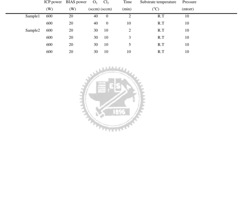
Table 2-1 The recipe for post-treatment process in oxygen and chlorine plasma ··· 44
Chapter 3
Table 3-1 AFM images of different catalysts growing at 700oC.··· 61 Table 3-2 Images of fluorescent screen monitoring the field electron emission from pillar array ··· 83 Table 3-3 Summary of Raman spectra for an as grown and CNT pillar array after O2 mix Cl2
plasma treatment. ··· 91 Table 3-4 EDS analysis ··· 92
Figure Captions
Chapter 1:
Figure 1-1 The SEM micrograph of (a) Spindt type triodes array, (b) Spindt type
Figure 1-2 Energy diagrams of vacuum-metal boundary: (a) without external electric field; and (b) with an external electric field.
field emission triode, (c) Emitting way of spindt type triode. [1.5]
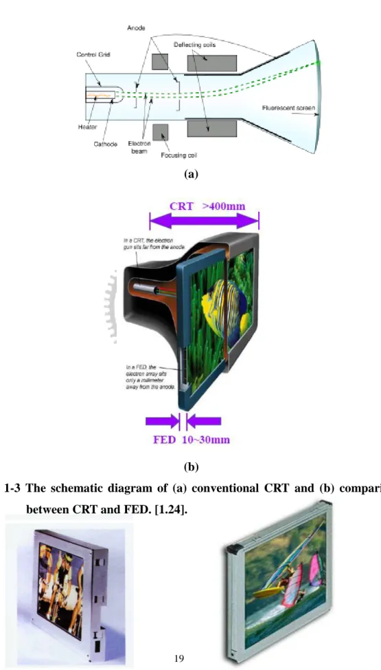
Figure 1-3 The schematic diagram of (a) conventional CRT and (b) comparison between CRT and FED. [1.24].
(b) Pixtech 5.6” color FED based on Spindt-type, (c) Futaba 7” color FED based
on Spindt-type, (d) Sony/Candescent 13.2” color FED based on Spindt-type, (e) Samsung 32“ under-gate CNT-FED, and (f) Canon-Toshiba 36” SED-TV.
Figure 1-5 (a) Si tip formed by isotropic etching and (b) Si tip field emission triodes array
formed by CMP [1.28] [1.29]
Figure 1-6 (a) The structure of SED, (b) SEM image of SCE cathode array, and (c) A 36-inch prototype of surface conduction electron emitter display. [1.30] [1.31]
Figure 1-7 High-resolution transmission electron microscopy images of (a) SWNTs, and (b) MWNTs. Every layer in the image (fringe) corresponds to the edges of each cylinder in the nanotube assembly [1.42].
Figure 1-8 Molecular models of SWNTs with (a) chiral vector (b) the categories of the configuration [1.45] [1.46].
Figure 1-9 (a) Schematic structure of the fully sealed 128 lines matrix-addressable CNT-FED. (b) Cross section SEM image of CNT cathode from Samsung’s FED.(c) A 4.5-inch FED from Samsung, the emitting image of fully sealed SWNT-FED at color mode with red, green, and blue phosphor columns. (d) A prototype of 5” CNT flat panel display by Samsung. [1.54]
Figure 1-10 The profile of LED backlight system (a) shows names of every sheet. [1.55] (b) direction of light beams in backlight system. (c) bottom lighting type of backlight system. (d) edge lighting type of backlight system. [1.56]
Chapter 2:
Figure 2-1 Simulation of the equipotential lines of the electrostatic field for tubes of different distances between tubes.
Figure 2-2 High Density Plasma Reactive Ion Etching System, HDP-RIE.[2.9] Figure 2-3 Schematic of a typical backlight unit.
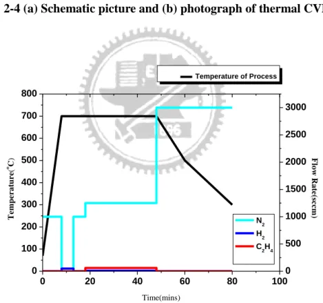
Figure 2-4 (a) Schematic picture and (b) photograph of thermal CVD.
Figure 2-5 Process of CNTs synthesis (an example of CNTs growing 30min at 700℃.
Figure 2-6 High vacuum measurement system.
Figure 2-7(a) SEM image of pillars of aligned CNT bundles grown by thermal CVD. (b) Cross-sectional SEM image of the pillar[2.12]
Figure 2-8 Masks design: (a)-(c) show array of three different inter-distance for 8 0μm、 150μm and 250μm defined in 1cm×1cm area, respectively.
Figure 2-9 Fabrication flow diagrams (a) ~ (j). (f) Co-Ti / Alcatalyst by sputtering system, (h) pretreatment with H2 (50 sccm), and (j) CNTs
Figure 2-10 (1) Process of two steps growing for CNTs’ synthesis. (2) Fabrication flow diagrams (a) ~ (e). (d) pretreatment in H2 at 50 sccm
Figure 2-11 Fabrication procedures for CNTs treated by plasma etching.
Figure 2-12 Schematic representation of fabrication procedures of triode structure. Figure 2-13 The under etching condition of N-type Poly-silicon by Die-electric Material
RIE 200L[2.13]
Figure 2-14 The aligned nanotubes in the bunch have variable heights and may protrude t hrough the gate opening, as shown in the figure, or lie beneath the gate electrode plane.[2.14]
Chapter 3:
Figure 3-1-1 Tilt AFM images of Co-Ti/Al catalyst growing nanoparticles during 5min at 700oC.
Figure 3-1-2 The schematic profiles of thin film catalyst change into nano-sized particle (a) without Al buffer layer (b) with Al buffer layer.
Figure3-1-3 Co-deposition catalyst of Co and Ti improved reliability obviously Figure 3-1-4 The surface energy effected on interface reaction.
Figure 3-1-5(a)Band structure of double-barrier model for field emission of CNT films. EFM
and EFCNT is the Fermi level of substrate metal and CNTs, respectively. Vjunction is
the voltage dropped on the substrate–CNTs junction.(b) Band structure of cathode for CNT films on titanium. The disappearing of interface
barrier was due to formation of conductive TiC interlayer.
Figure 3-1-6 Sketch for side-contact of CNT and electrode. (a) Electrons tunnel through finite energy barrier created by oxide at CNT–metal interface. (b) Electrons can transport into CNT smoothly through conductive TiC layer at CNT–Ti interface. Figure 3-1-7 AFM images of different catalysts growing at 700oC.
Figure 3-2-1 (a)~(g) SEM images of aligned CNT pillar array in inter-distance of 80μ m for (a)R/H=18.18,(b)R/H=11.2,(c)R/H=8,(d)R/H=7.8,(e)R/H=6.06,(f)R/H=3.6, (g)R/H=1.5.
Figure 3.2.2 (a)~(g) SEM image of aligned CNT pillar array in inter-distance of 150μm for(a)R/H=10.7,(b)R/H=7.5,(c)R/H=6,(d)R/H=4.7,(e)R/H=3.2,(f)R/H=2.5,
(g)R/H=1.87.
Figure 3-2-3 (a)~(e) SEM images of aligned CNT pillar array in inter-distance of 250μm for (a)R/H=14,(b)R/H=10,(c)R/H=5.1,(d)R/H=3.1,(e)R/H=2.5.
Figure 3-2-4 Length of the aligned CNTs as a function of formation time (a) with 60sccm flow for C2H4, (b) with 135sccm flow for C2H4.
Figure 3-2-5 (a)Plot of the FE current density versus the applied electric field (b) current density in log scale versus the applied electric field (c) the corresponding F–N plots of CNT pillar array synthesized in pattern of inter-distance 80μm .
Figure 3-2-6 Variation of (a) turn-on field (Eto) and (b) field-enhancement factor (β)
with the ratio of inter-distance (80μm) to pillar height (H) .
Figure3-2-7 (a)Plot of the FE current density versus the applied electric field (b) current density in log scale versus the applied electric field (c) the corresponding F–N plots of CNT pillar array synthesized in pattern of inter-distance 150μm .
Figure 3-2-8 Variation of (a) turn-on field (Eto) and (b) field-enhancement factor (β)
with the ratio of inter-distance (150μm) to pillar height (H) .
Figure 3-2-9 (a)Plot of the FE current density versus the applied electric field (b) current density in log scale versus the applied electric field (c) the corresponding F–N plots of CNT pillar array synthesized in pattern of inter-distance 250μm.
Figure 3-2-10 Variation of (a) turn-on field (Eto) and (b) field-enhancement factor (β)
with the ratio of inter-distance (250μ m) to pillar height (H) .
Figure 3-2-11 Optimal R/H value for the height of CNT pillar to inter-pillar distance ratio. Figure 3-2-12 Field emission property of different inter-pillar distances with R/H values of
about 5.5
Figure 3-3-1 SEM analysis for one-step growth. Figure 3-3-2 SEM analysis for two-step growth.
Figure 3-3-3 Analysis diameters for one-step and two-step growth.
Figure 3-3-4 The Raman spectra of direct growth CNT pillar and two-step growth CNT pillar array.
Figure 3-3-5 Field emission properties of pillars of aligned CNT bundles: (a) current density-electric field plot, (b) current density in log scale versus electric field plot and (c) Fowler-Nordheim plot.
Figure 3-3-6 Image of fluorescent screen monitoring the field electron emission from the pillar array (10mm × 10mm) at an electric field of 0.66 V/μm.
Figure 3-3-7 TEM analysis
Figure 3-4-1 SEM images after post-treatment of pure oxygen in the top view (a) 2min (b) 10min.
Figure 3-4-2 SEM images after post-treatment of pure oxygen in the cross-section view. Figure 3-4-3 SEM images after post-treatment of oxygen mix chlorine for 2 min (a) (b) in the
tilt view (c) in the top view (d) oxygen mix chlorine compound around the CNTs.
Figure 3-4-4 SEM images after post-treatment of oxygen mix chlorine for 3 min (a) in the tilt view (b) in the top view.
Figure 3-4-5 SEM images after post-treatment of oxygen mix chlorine for 5 min (a) in the cross-section view (b) at the tip of the pillar.
Figure3-4-6 SEM images after post-treatment of oxygen mix chlorine for 10 min (a) in the tilt view (b) in the top view.
Figure 3-4-7 Raman spectra of pillar sample after O2 mix Cl2 plasma post-treatment obtained
using 514.5nm excitations. The inset image is an optic microscope image at the top of a pillar.
Figure 3-4-9 Plot of the IG/ID versus the time for O2 plus Cl2 plasma post-treatment.
Figure 3-4-10 EDS spectra for the nanoparticles at the tip of the CNT.
Figure 3-4-11Field emission current density vs electric field for a vertically aligned CNT pillar array (a) after O2 plasma post-treatment and (b) after O2 mix Cl2 plasma post-treatment.
Figure 3-4-12 Image of fluorescent screen monitoring the field emission from the pillar array (10mm×10mm) at an electric field of 3.33V/μ m.
Figure 3-5-1 Central CNTs were used to be cathode electric emitter, and surrounding N-type poly-Si was used to be gate of this triode structure by Simulation.
Figure 3-5-2 Cross-section view for the nanotriode 3D model used for computing the electric field with Simion 3D 7.0. The aligned nanotubes in the bunch have variable heights and may protrude through the gate opening, as shown in the figure, or lie beneath the gate electrode plane.(a) electric field emission without gate structure.(b) electric field emission with 35V gate voltage supplied.
Figure 3-5-3 Equipotential lines near CNT tips – detail with the gate supplied 35V.
Figure 3-5-4 The corresponding cross-sectional SEM micrographs showing the CNT lengths of (a) 0.5μm and (b) 1μm. Inset image is triode structure with 9μm
inter-distance after CNTs growth.
Figure 3-5-5 The SEM images micrographs showing the CNT lengths of 5μm (a)(e)tilt image (b)cross-section view for triode pillar array (c)(d) the gate-to-emitter gap kept at 0.8μ m (f) few CNTs shorted gate to cathode
Figure 3-5-6 The corresponding JA-VB plots of the CNT triodes for 1μm and 5μm of
nanotubes.
Figure 3-5-7 The corresponding F-N plots of the CNT triodes for 1μm of nanatubes
Figure 3-5-8 Images of fluorescent screen monitoring the field electron emission from the CNT triode array (3mm × 3mm) at the gate voltage (a) 20 V, (b) 30 V , respectively.
Chapter 1
Introduction
1.1 Overview of Vacuum Microelectronics
In 1991, carbon nanotubes (CNTs) were discovered by Sumio lijima who observed hollow carbon nanotubes by TEM. Since the diameter of nanotubes is on the order of a few nanometers, and the length can be up to several micrometers, they have very height-to-diameter ratios. Carbon nanotubes are cylindrical carbon molecules with novel properties that make them potentially used in nano-electronics and optics etc. Due to the nanometer-sized , hollow center, and large surface area﹐CNTs are ideal field emission sources and used in vacuum microelectronics.
1.1.1 History of Vacuum Microelectronics
In 1948, vacuum tubes have been gradually replaced by solid state devices, which tiny volume, low cost, better reliability, and more power efficient transistors were invented by John Bardeen, Walter Bratain, and William Shockley [1.1].
But nowadays, there has been a growing interest in vacuum microelectronics. Some reasons for the increasing interest have to do with the superior theoretical electrical characteristics of the vacuum microelectronic devices over semiconductor devices. The so called vacuum microelectronic devices using the professional micro fabrication technology have been successfully fabricated and gave a new life to vacuum electronics due to great improvements on semiconductor manufacturing technology for the past decades.
“Vacuum state” devices have many superior advantages with respect to the present “solid state” devices, including radiation hardness, temperature insensitivity, and fast drift velocity. For example, there is negligible radiation effect in vacuum devices due to medium being damaged as the electrons fly in the vacuum [1.2].
Moreover, there is no medium for electrons fly in the vacuum, so there is no lattice scattering or bulk carrier generation/recombination. Therefore, the vacuum microelectronic devices can suffer to 500 ℃ or above as long as the structures of the vacuum devices do not destroyed and greatly reduced (nearly eliminated) temperature
sensitivity problem which usually comes along with semiconductor devices. Additionally, the saturation drift velocity is limited to less than 3107 cm/s in all semiconductor due to scattering mechanism whereas the saturation drift velocity in vacuum is limited theoretically to 31010 cm/s and practically to about 6-9108 cm/s [1.3].
Table 1-1 shows the comparison between vacuum microelectronic and
semiconductor devices. Vacuum electronics can be broadly separated into two categories: Thermionic emission or Field emission. The theory of field emission started in 1928, when R. H. Fowler and L. W. Nordheim published the first theory of electron field emission (Fowler- Nordheim theory) from metals using quantum mechanics [1.4]. The difference concerns the way electrons are emitted from the cathode. Thermionic emission relies on a heated electron emitter, or cathode. The cathode is heated up enough such that the electrons receive enough kinetic energy to leave the surface of the cathode. Field emission, unlike thermionic emission, is possible with a cold cathode. Field emission is a form of quantum tunneling in which electrons pass through a barrier in the presence of a high electric field. This phenomenon is highly dependent on both the properties of the material and the shape of the particular cathode, so that higher aspect ratios produce higher field emission currents. According to the Fowler-Nordheim theory, an applied electric field of approximately 103 V/m is needed for electrons to tunnel through the sufficiently narrow barrier [1.2]. To reach this high field at reasonable applied voltage, it is customary to machine the field emitters into protruding objects to take advantage of field enhancement.
It was not until 1968 when C. A. Spindt camp up with a fabrication method to create very small dimension metal cones that vacuum microelectronic triodes became possible [1.2]. Fig.1-1 is a schematic diagram of the triode fabricated by Spindt [1.5]. From the late 1960s to the year 1990, Ivor Brodie, Henry F. Gray, and C. A. Spindt made many contributions to this field. Also, most of research was focused on the devices similar to the Spindt cathode during the past three decades.
In 1991, a group of research of the French company LETI CHEN reported a microtip display at the fourth International Vacuum Microelectronics Conference [1.6]. Their display was the first announcement of a practical vacuum microelectronic device. From then on, a great amount of researchers all over the world devoted themselves to this
interesting, challenging, and inventive field. Part of the work focused on fabricating very small radius silicon tip by utilizing modern VLSI technology [1.7-1.8]. Some of them increased the emission current by coating different metals, such as W, Mo, Ta, Pt etc., even diamond on field emission arrays [1.9-1.10]. Different device schemes also have been proposed to enhance the emission current density, stability, and reliability.
1.1.2 Theory Background
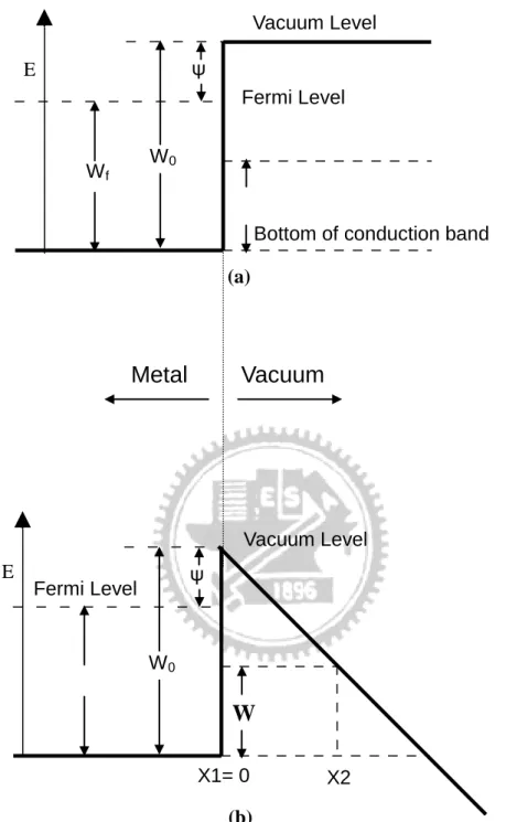
In quantum mechanical, electron field emission is a tunneling phenomenon of electrons extracted from the conductive solid surface, such as a metal or a semiconductor, where the surface electric field is extremely high.
If a sufficient electric field is applied on the emitter surface, electrons will be emitting through the surface potential barrier into vacuum, even under a very low temperature. On the other hand, thermionic emission is the hot electron emission under high temperature and low electric field. Fig. 1-2(a) demonstrates the band diagram of a metal-vacuum system.
Here W0 is the energy difference between an electron at rest outside the metal and an
electron at rest inside, whereas Wf is the energy difference between the Fermi level and
the bottom of the conduction band. The work function is defined as = W0 - Wf. If an
external bias is applied, vacuum energy level is reduced and the potential barrier at the surface becomes thinner as shown in Fig. 1-2(b).
Figure 1-2 Energy diagrams of vacuum-metal boundary: (a) without external electric field; and (b) with an external electric field.
Vacuum
Metal
Bottom of conduction band Fermi Level ψ E Vacuum Level Fermi Level ψ Vacuum Level X1= 0 X2 (b) (a) Wf W0 E W0
W
Then, an electron having energy “W” has a finite probability of tunneling through the surface barrier. Fowler and Nordheim derive the famous F-N equation (1.1) as follow [1.2]:
e x p [ 2 ( )/ ] 3 2 2 E y v b y t aE J , (1-1)where J is the current density (A/cm2). E is the applied electric field (V/cm), is the work function (in eV), a = 1.5610-6, b = -6.83110-7, y = 3.79x10-410-4E1/2/, t2(y)~1.1 and v(y) can be approximated as [1.10]
v(y)cos(0.5y), (1-2) or
v(y)0.95y2. (1-3)
Typically, the field emission current I is measured as a function of the applied voltage V. Substituting relationships of J = I/ and E = V into Eq.(1-1), where is the emitting area and is the local field enhancement factor of the emitting surface, the following equation can be obtained
exp[ ( ) ] ) ( 2 3 2 2 2 V y bv y t V A I . (1-4) Then taking the log. form of Eq. (1-4) and v(y) ~ 1
] 2.97 10 ( ( )) ) ( 10 54 . 1 log[ ) log( 2 3 7 2 2 6 2 V y v y t V I , (1-5)
from Eq. (1-5), the slope of a Fowler-Nordheim (F-N) plot is given by
2.97 10 ( ) 2 3 7 slopeFN S , (1-6)
The parameter can be evaluated from the slope S of the measured F-N plot if the work function was known
2.97 10 ( ) 2 3 7 S (cm-1), (1-7) The emission area can be subsequently extracted from a rearrangement of Eq.(1-5)
exp( 9.89)exp(6.53 10 ) 10 4 . 1 ) ( 2 3 7 2 6 2 V V I (cm2). (1-8)
For example, the electric field at the surface of a spherical emitter of radius r concentric with a spherical anode (or gate) of radius r+d can be represented analytically by
( ) d d r r V E , (1-9) Though a realistic electric field in the emitter tip is more complicated than above equation, we can multiply Eq.(1-9) by a geometric factor ` to approximate the real condition. Etip function of (r,d) =` ( ) d d r r V , (1-10)
where r is the tip radius of emitter tip, d is the emitter-anode(gate) distance and ` is a geometric correction factor [1.11].
For a very sharp conical tip emitter, where d >> r, Etip approaches to `(V/r). And
for r>>d, Etip approaches to `(V/d) which is the solution for a parallel-plate capacitor
and for a diode operation in a small anode-to-cathode spacing.
As the gated FEA with very sharp tip radius, Eq. (1-10) can be approximated as:
Etip=`(V/r), (1-11). Combining E = V and Eq. (1-11), we can obtain the relationship:
Etip =V =`(V/r), and `= r., (1-12) The tip radius r is usually in the range from a few nm to 50 nm, corresponding to the
Besides, transconductanceg of a field emission device is defined as the change in m
anode current due to the change in gate voltage [1.1].
g C m V I g |Vc, (1-13)
Transconductance of a FED is a figure of merit that gives as an indication of the amount of current charge that can be accomplished by a given change in grid voltage. The transconductance can be increased by using multiple tips or by decreasing the gate-to-cathode spacing for a given anode-to-cathode spacing.
The following approaches may therefore be taken to reduce the operating voltage of the field emission devices according to the equations above mentioned:
a. Narrow the cone angle for increasing
b. Reproducibly sharpen the tips to the atomic level for increasing c. Choose the tip material which has the lower work function () d. Reduce the gate-opening diameter for increasing.
1.2 Applications of Vacuum Microelectronic Devices
Due to the superior properties of vacuum microelectronic devices, potential applications include high brightness flat-panel display [1.12-1.16], high efficiency microwave amplifier and generator [1.17-1.19], ultra-fast computer, intense electron/ion sources [1.20-1.21], scanning electron microscopy, electron beam lithography, micro-sensor [1.22-1.23], temperature insensitive electronics, and radiation hardness analog and digital circuits
1.2.1 Vacuum Microelectronic Devices for Electronic Circuits
Either vacuum or solid-state devices can generate power at frequency in the GHz range. Solid-state devices, such as impact avalanche transit time (IMPATT) diodes, Si
bipolar transistors, and GaAs FETs [1.24], are typically used in the lower power (up to 10 W) and frequency (up to 10 GHz) range. Vacuum devices still remain the only technology available for high power and high frequency applications. These devices include traditional multi-terminal vacuum tubes, like triodes, pentodes, and beam power tubes, and distributed-interaction devices, such as traveling wave tubes (TWTs), klystrons, backward-wave oscillators (BWOs).
The performance of FEAs in conventionally modulated power tubes, like TWT, is determined primarily by their emission current and current density capability. On the other hand, application of FEAs in the microwave tubes in which modulation of the beam is accomplished via modulation of the emission current at source, such as capacitance and transconductance. Successful operation of a gated FEA in a 10 GHz TWT amplifier with conventional modulation of electron beam has been demonstrated by NEC Corporation of Japan [1.25]. The amplifier employed a modified Spindt-type Mo cathode with circular emission area of 840 m in diameter. The modified cathode structure incorporated a resistive poly-Si layer as a current limiting element. The emission current from the cathode was 58.6 mA. The prototype TWT could operate at 10.5 GHz with the output power of 27.5 W and the gain of 19.5 dB. The bandwidth of the tube was greater than 3 GHz. The prototype was operated for 250 h.
1.2.2 Field Emission Displays
Among wide range applications of the vacuum microelectronics, the first commercial product could be the field emission flat-panel display. The field emission fluorescent display is basically a thin cathode ray tube (CRT), which was first proposed by SRI International and later demonstrated by LETI [1.6].
Various kinds of flat-panel displays, such as liquid crystal display (LCD), electroluminescent display (EL), vacuum fluorescent display (VFD), plasma display panel (PDP), and light emitting display (LED), are developed for the better characteristics of small volume, light weight, and low power consumption. LCDs have become the most popular flat panel displays, however, LCDs have some drawbacks, such as poor viewing angle, temperature sensitivity and low brightness. As a result, some opportunities still exist and waiting for the solutions from other flat panel displays such as FED.
FED features all the pros of the CRTs in image quality and is flat and small volume. The schematic comparisons are revealed in Fig. 1-3 [1.24]. The operation of CRTs involves deflection of the beam in such a way that the electron spot scans the screen line-by-line. In FEDs, multiple electron beams are generated from the field emission cathode and no scanning of beams is required. The cathode is a part of the panel substrate consists of an X-Y electrically addressable matrix of field emission arrays (FEAs). Each FEA is located at the intersection of a row and a column conductor, with the row conductor serving as the gate electrode and the column conductor as the emitter base. The locations where the rows and columns intersect define a pixel. The pixel area and number of tips are determined by the desired resolution and luminance of the display. Typically, each pixel contains an FEA of 4-5000 tips. The emission current required for a pixel varies from 0.1 to 10 A, depending on the factors such as the luminance of the display, phosphor efficiency and the anode voltage.
Compared to the active matrix LCDs and PDPs, FEDs are energy efficient and could provide a flat panel technology that features less power consumption. They can also be cheaper to make, as they have fewer total components. Moreover, FEDs could generate three times the brightness with wilder viewing angle at the same power level. Full color FEDs have been developed by various research groups from different aspects such as Motorola, PixTech, Futaba, Sony/Candescent, Samsung, and Canon-Toshiba are presently engaged in commercially exploiting FEDs. the products of above mentioned companies are shown in Fig. 1-4.
1.2.3 Cathode Structure and Materials for Field Emission Displays
Field emission display is one of the most promising emissive type flat-panel displays, which can overcome the drawbacks of TFT-LCD, such as poor viewing angle, temperature sensitivity, low contrast and low brightness. This section introduces some novel cathode structures and synthesizes these novel emitter materials for FED operations
1.2.3.1 Spindt-type Field Emitters
The “Spindt” cathode was first proposed by C. A. Spindt in 1968 [1.25]. The scanning electron microscope (SEM) image of a spindt type field emission triode has
been shown in Fig. 1-1 agian. It was first invented by Spindt of SRI and improved for the electron source of high-speed switching devices or microwave devices [1.2]. In 1970s, Meyer of LETI applied Spindt-typed emitters for a display and introduce a resistive layer as the feedback resistance to stabilizing the field emission from Spindt-type emitters [1.26].
The structure of Spindt-type FED includes a substrate, a cathode electrode of an electron emission unit formed thereon having a substantially conical shape, and a gate electrode of a lead-out electrode stacked on a substrate around the cathode electrode having an insulating layer. In the Spindt type FED a voltage is applied between the cathode electrode and the gate electrode in a vacuum to thereby produce a high electric field. As a result, electrons are emitted from a tip end of the cathode electrode through the electron emission mechanism in an electric field. In addition, the Spindt-type FED has a conical electron emission portion formed on a cathode electrode. It higher electron drawing efficiency since the electron emission portion is arranged in the vicinity of the center of the gate electrode where the electric field is most concentrated, and the directivity of electron emission is regular.
The merits of the Spindt-type field emitters are summarized as following: (1) High emission current efficiency, more than 98 % anode current to cathode current can be achieved for the symmetric structure of Spindt tip and the gate hole, the lateral electric field to the metal tip can be cancelled out. (2) The fabrication is self-aligned, easy process; uniform field emission arrays can be fabricated easily. Some research groups have successfully fabricated commercial FED products based on Spindt-type field emitters such as motorola, Pixtech, Futaba and Sony/Candesent.[1.27], the products of above mentioned companies are shown in Fig. 1-4.
However, there are some drawbacks of Spindt-type field emitters when fabricating Spindt-type FED such as (1) High gate driving voltage required; for a Spindt-type field emission triode with 4 m gate aperture, the driving voltage is typically more than 60 V, which results in the high cost of the driving circuits. To reduce the gate driving voltage, frontier lithography technologies such as E beam lithography must be applied to reduce the gate aperture to the sub-micron level. (2) The emission property degrades for the chemically instable of the metal tips. (3) Huge, expensive high vacuum deposition system
required during fabricating large area Spindt-type FED.
1.2.3.2 Silicon Tip Field Emitters
An alternative approach to fabricate tip type field emitters is to fabricate the Si tip field emitters based on the semiconductor fabricating process. Figure 1-5 depicts the SEM micrographs of Si tips array, Si tip field emission triodes array formed by chemical mechanical polishing (CMP) [1.28] and double gate of Si field emitter arrays [1.29]. Symmetric device structure and similar advantages with Spindt-type field emitters can be obtained. However, high temperature oxidation sharpening process prohibits Si tip from large area fabrication
1.2.3.3 Surface Conduction Electron Emitters
A surface conduction electron emitter (SCE) display is a flat panel display technology that uses surface conduction electron emitters for every individual display pixel. The surface conduction emitter emits electrons that excite a phosphor coating on the display panel, the same basic concept found in traditional CRT televisions. The key technology to the electron emitters begins with the creation of an extremely narrow slits (~ several nanometers) between two electric poles in thin film of PdO (Palladium Oxide). Electrons are emitted from one side of the slit when approximately 10 V of electricity are applied. Some of these electrons are scattered at the other side of the silt and accelerated by the voltage (approximately 10 kV) applied between the glass substrates; causing light to be emitted when they collide with the phosphor-coated glass plate. The PdO film is coated by inject printing or screen-printing technology and this is a low cost process. This means that SEDs use small cathode ray tubes behind every single pixel (instead of one tube for the whole display) and can combine the slim form factor of LCDs and plasma displays with the superior viewing angles, contrast, black levels, color definition and pixel response time of CRTs. The major problem of SED is that the efficiency is still low and the power consumption will be very high. Fig. 1-6 shows the SEM image of SCE cathode array, structure and a 36-inch display of SED [1.30][1.31].
The research of SED was began by Canon in 1986, and in 2004, Toshiba and Canon announced a joint development agreement originally targeting commercial production of
SEDs. In October 2006, Toshiba's president announced the company plans to begin full production of 55" SED TVs in 2007. In December 2006, Toshiba President and Chief Executive Atsutoshi Nishida said Toshiba is on track to mass-produce SED TV sets in cooperation with Canon by 2008.
1.2.3.4 Carbon and Nano-sized Emitters
So-called carbon nanotubes (CNTs) is the nano-sized and carbon emitters, is known to be useful for providing electron emission in field emission devices, such as cold cathodes that are used in a field emission display. Although Spindt-type emitters are generally used for FEDs, they still have a problem in that the life span of micro-tips is shortened due to atmospheric gases or a non-uniform field during a field emission operation. Moreover, the work function of the conventional metal emitters is too high to decrease a driving voltage for field emission. To overcome the problem, CNTs which have a substantially high aspect ratio, excellent durability due to their structure and excellent electron conductivity have been instead of Spindt-type emitters for field emission. CNTs are are anticipated to be an ideal electron emission source since they feature a low work function, the resultant electron emission source can be driven by applying low voltages, and the method of fabricating the same is not complicated. They will thereby offer advantages to realize a large size panel display in terms of view angle, definition, power consumption, and temperature stability.
1.3 Field Emission Properties of Carbon Nanotubes
Since the discovery of carbon nanotubes (CNTs) by Iijima in 1991, [1.32] CNTs have attracted considerable interests because of their unique physical properties and many potential applications [1.33]. CNTs have numerous potential applications in nanoelectronics, nanometer-scale structural materials, hydrogen storage, field-emission devices, and so on. Among these applications, CNTs seem to be very promising as electron emitters for field-emission displays (FEDs).
Carbon nanotubes (CNTs) have been extensively investigated for the synthesis using arc discharge, laser vaporization, pyrolysis, solar energy, and plasma-enhanced chemical vapor deposition (CVD), for its unique physical and chemical properties and for applications to nanoscale devices. However, common methods of CNT synthesis include: (1) arc-discharge [1.34], (2) laser ablation [1.35], (3) thermal CVD [1.36-1.38], and (4) plasma enhanced CVD [1.39][1.40].
The laser ablation can synthesize pure carbon nanotubes in high fabrication temperature, but large scale display panel can not be fabricated in the high fabrication temperature above the melting point of glass substrate. The arc discharge can synthesize carbon nanotubes in shorter fabrication times, but it has some issues, such as (1) poor purity, (2) hard to control growth orientations of carbon nanotubes, and (3) poor emission uniformity.
Compared to laser ablation and arc discharge, using CVD for carbon nanotube growth has some features, such as (1) high purity carbon nanotubes, (2) selective growth only for catalyst metal, (3) controlling growth direction, and (4) much suitable to semiconductor fabrication procedure. However, with the display technology trend, it is the time for large panel display. We need to synthesize carbon nanotubes using CVDs on large panel substrates. For this reason, carbon nanotube growth at low temperatures is unavoidable, but the purity of carbon nanotubes at low temperatures is poor. So, we still try some methods to increase growth rates at low temperatures, such as (1) multilayer catalysts, (2) plasma CVDs, (3) post-treatment, and so on.
1.3.2 Structure and Properties of Carbon Nanotubes
CNTs can be divided into two categories. The first is called multiwalled carbon nanotubes (MWNTs). MWNTs are close to hollow graphite fibers [1.41], except that they have a much higher degree of structural perfection. They are made of sheets of carbon atoms with a cylindrical shape and generally consist of co-axially arranged 2 to 20 cylinders「Fig. 1-7(b)」. The interlayer spacing in MWNT (d(002) = 0.34 nm) is slightly
larger than that in single crystal graphite (d(002) = 0.335 nm) [1.42]. This is attributed to a
combination of tubule curvature and van der Waals force interactions between successive garphene layers. The second type of the nanotube is made up of just a single layer of
carbon atoms. These nanotubes are called the single-walled nanotubes (SWNTs) and possess good uniformity in diameter about 1.2 nm Fig.[1-7(a)]. They are close to fullerenes in size and have a single-layer cylinder extending from end to end [1.43][1.44]. Most experimentally observed CNTs are multi-walled structures with outer most shell diameters exceeding 10 nm. Since current conduction in a MWNT is known to be mostly confined to the outermost single-walled nanotube and since band gap of a SWCNT varies inversely with its diameter, MWNTs are metallic in nature. SWNTs can be either metallic or semiconducting depending on the way the roll-up of the graphene sheet occurs - an aspect termed as Chirality, and if all the roll-up types are realized with equal probability, 1/3 of the SWNTs end up being metallic and 2/3 semiconducting. The structure of a SWNT can be conceptualized by wrapping a one-atom-thick layer of graphite called graphene into a seamless cylinder. The way of the graphene sheet is wrapped is represented by a pair of indices (n,m) called the chiral vector. The integers n and m denote the number of unit vectors along two directions in the honeycomb crystal lattice of graphene. If m=0, the nanotubes are called "zigzag". If n=m, the nanotubes are called "armchair". Otherwise, they are called "chiral". Fig. 1-8 depicts these structures of a SWNT [1.45] [1.46].
CNTs have been attracting much attention for their unique physical and chemical properties such as high mechanical strength, chemical stability, high aspect ratio, super-therml conductivity, and electron emission properties [1.47] [1.48]. CNTs could be one of the strongest and stiffest materials known, in terms of tensile strength and elastic modulus respectively. This strength results from the covalent sp2 bonds formed between the individual carbon atoms. The highest tensile strength an individual multi-walled carbon nanotube has been tested to be is 63 GPa [1.49]. Under excessive tensile strain, the tubes will undergo plastic deformation, which means the deformation is permanent. This deformation begins at strains of approximately 5% and can increase the maximum strain the tube undergoes before fracture by releasing strain energy. For the thermal conductivity of CNTs , it is predicted that carbon nanotubes will be able to transmit up to 6000 watts per meter per kelvin at room temperature; compare this to copper, a metal well-known for its good thermal conductivity, which only transmits 385 W/m/K. The temperature stability of carbon nanotubes is estimated to be up to 2800 degrees Celsius in
vacuum and about 750 degrees Celsius in air [1.50].
1.3.3 Potential Applications of Carbon Nanotubes
Since the discovery of CNTs in 1991, CNTs had attracted much attention for their unique physical and chemical properties. Their extensively potential applications lead them to become a super star of nano technology, which cover: (1) Chemical sensor [1.51], (2) IR detector, (3) Nano-conducting Wire, (4) Vehicles for Hydrogen Storage [1.52], (5) Field Effect Transistor [1.53], (6) Field Emission Display (FED), (7) Probe of AFM and etc.
In the wide-ranging applications of CNTs, FED arouses researchers’ interest particularly. In virtue of the superior field emission characteristics, CNTs are applied to the emitting source of cold cathode. The advantages of FED are its low response time, wide view angle, high brightness, high working temperature range and well combination with mature phosphor technology. However, a major problem needs to be solved in this field. It is not allowed to effectively analyze CNTs on a flat panel at relatively lower temperature (<500˚C) and this barrier restriction obstructs the development of CNT-FED so far. The products of CNTs FED is shown in Fig. 1-9.
1.4 Motivation
For technological commercialization of products today, the cost is the most important issue. The main concern for manufactures is cost down. It is worth noted that lower cost will provide more advantages for a product. In our research of CNT field-emission backlight unit (FE-BLU), we ensure that if the cost of field-emission backlight unit (FE-BLU) continuously decreases, it can even replace the traditional light bulbs or light-emitting diode (LED) in the future. So the following motivation will focus on decreasing the cost and increasing the quality of CNT FE-BLU.
Nowadays, the backlight unit of liquid crystal display (LCD) is CCFL, but CCFL backlight system contains several components for providing planar and uniformity illumination. The following are designs of LED-BLU:
lamp.
2. Light guide panel is used to transform spot or linear light source to planar light source.
3. The prism sheet and diffusion sheet are playing the crucial roles in spreading the brightness.
Fig. 1-10 shows the complex system of LED backlight unit on LCD below [1.55] [1.56]. The uniformity become better due to the uniformity-assisted layer of backlight system, but thickness and cost increase obviously. For a LCD, the cost of backlight system on the total cost is about 14% for 17inch TFT-LCD, and 21% for 32inch TFT-LCD, which are shown in Fig. 1-11 [1.57]. As this result, we could easily to make a prediction that we will require more cost on backlight system for a larger size TFT-LCD.
Many relative researches for the synthesis or the field-emission characteristics improvements of the carbon nanotubes-based field-emission devices have been reported so far. However, only few of them discussed the problems of reliability and uniformity in the field-emission devices. For the purpose of applications, the issues of reliability and uniformity are two of the most critical keys for the commercialization of field-emission displays and back-light units. Therefore, we focus on the issue of uniformity of the carbon nanotubes-based field-emission devices. Furthermore, the increase of emission current density and power efficiency of the carbon nanotubes-based field-emission devices are also discussed here (in Chapter 2 and Chapter 3).
1.4.1 Uniformity
Uniformity is the most difficult challenge for the applications of field-emission displays and back-light units, especially for the displays with image size. Due to the difficulty of controlling the diameter, length, direction, and distribution of the carbon nanotubes, it is still hard to obtain a uniform emission current from the carbon nanotubes-based field-emission devices. In Chapter 2 Experiment A, man-made emitters are defined by lithography to control the morphologies and distribution of the emitters. In Chapter 2 Experiment C, try to improve uniformity of field-emission displays by plasma post-treatment.In Chapter 2 Experiment D, triode emitters are defined by lithography to control the morphologies and gate-control distribution of the emitters precisely.
1.5 Thesis Organization
The overview of vacuum microelectronics, field emission display and basic principles of field emission theory was described in chapter 1.
The experimental procedures were revealed in chapter 2. First, we utilize three types of different inter-pillar distance patterns, such as 80, 150 and 250 μm then use them on silicon substrate to compare their morphology and discussion their uniformity. We discussed the effect of R/H ratios of CNTs pillars. In the part, we investigated and found the relations of R/H ratios (inter-pillar spacing (R)/pillar height (H) ratios) to obtain the optimization and perimeter of the field emission characteristics. We also post-treat CNT pillar array by plasma bombardment and find the optimal condition of plasma. Finally, try to enhance emission electron from triode-pillar array by gate voltage.
Results and discussion were summarized in chapter 3. then, we accomplished many important results including, (1) SEM images, (2) TEM images, (3) AFM images, (4) Raman analysis, (5) EDS analysis, and (7) Field Emission Measurement.
Table 1-1
Comparison between vacuum microelectronics and solid-state electronics.
Items
Solid State Microelectronics
Vacuum Microelectronics Current Density 104 – 105 (A/cm2) similar Turn-on Voltage 0.1 – 0.7 V 5 – 300 V
Structure solid/solid interface solid/vacuum interface Electron Transport in solid in vacuum Electron Velocity 3107 (cm/sec) 31010 (cm/sec) Flicker Noise due to interface due to emission Thermal & Short Noise comparable comparable Electron Energy < 0.3 eV a few to 1000 eV Cut-off Frequency < 20 GHz (Si) &
100 GHz (GaAs)
< 100 – 1000 GHz Power small – medium medium – large Radiation Hardness poor excellent Temperature Effect -30 – 50 C < 500 C Fabrication & Materials well established (Si) &
fairly well (GaAs)
not well established
field emission triode, (c) Emitting way of spindt type triode. [1.5]
(a)
(b)
Figure 1-3 The schematic diagram of (a) conventional CRT and (b) comparison between CRT and FED. [1.24].
(a) (b)
(c) (d)
(e) (f)
Figure 1-4 The full color FED products: (a) Motorola 5.6” color FED based on Spindt-type , (b) Pixtech 5.6” color FED based on Spindt-type, (c) Futaba 7” color FED based on Spindt-type, (d) Sony/Candescent 13.2” color FED based on Spindt-type, (e) Samsung 32“ under-gate CNT-FED, and (f) Canon-Toshiba 36” SED-TV.
(a)
(b)
Figure 1-5 (a) Si tip formed by isotropic etching and (b) Si tip field emission triodes array formed by CMP [1.28] [1.29]
t (b) (c)
Figure 1-6 (a) The structure of SED, (b) SEM image of SCE cathode array, and (c) A 36-inch prototype of surface conduction electron emitter display. [1.30] [1.31]
(b)
Figure 1-7 High-resolution transmission electron microscopy images of (a) SWNTs, and (b) MWNTs. Every layer in the image (fringe) corresponds to the edges of each cylinder in the nanotube assembly [1.42].
(b)
Figure 1-8 Molecular models of SWNTs with (a) chiral vector (b) the categories of the configuration [1.45] [1.46].
(a)
(b)
Figure 1-9 (a) Schematic structure of the fully sealed 128 lines matrix-addressable CNT-FED. (b) Cross section SEM image of CNT cathode from Samsung’s FED.(c) A 4.5-inch FED from Samsung, the emitting image of fully sealed SWNT-FED at color mode with red, green, and blue phosphor columns. (d) A prototype of 5” CNT flat panel display by Samsung. [1.54]
(a)
(b)
(c) (d)
Fig 1.10 The profile of LED backlight system (a) shows names of every sheet. [1.55] (b) direction of light beams in backlight system. (c) bottom lighting type of backlight system. (d) edge lighting type of backlight system. [1.56]
(b)
Chapter 2
Experimental Procedures
2.1 Introduction
Carbon nanotubes (CNTs) are one of the field-emission materials because of their high geometric aspect ratio, small tip radius of curvature, high electrical conductivity, high mechanical strength, and chemical stability[2.1].So far, the usefulness of electron sources using a CNT emitter as a cold cathode has been demonstrated for vacuum electronic devices such as field-emission displays[2.2][2.3], backlight sources[2.4], and x-ray tubes[2.5]. For such device applications, CNT emitters are required to possess a low driving voltage and durability for a long lifetime.In recent years, CNT emitters have been fabricated by two main methods: chemical vapor deposition (CVD)[2.6] and screen printing[2.4]. In both methods, it is important to control the length and the inter-tube distance of CNTs to reduce the screening effect in adjacent CNTs[2.7] shown in Fig.2.1. It has been reported that field emission can effectively enhanced for aligned CNTs as field emitters when the ratio of the inter-tube distance to the height of each CNT is about 2[2.8], but, in our research, the ratio of the inter-tube distance to the height of each CNT is not approximately 2. However, the reduction of the field screening effect, and the optimal ratio of the inter-tube distance to the height which are components of an efficient field emitter, has not been sufficiently investigated.
Reports have stated that field emission is dependent on the direct parameters of CNTs such as the number of walls, the shape and structure of the tips, and indirect parameters such as surface treatment and CNT-alignment methods on a substrate. Recent works on CNT field emission are focused on several post-treatment methods and new growth method of CNTs to improve the uniformity and density of the electron emission site. Plasma surface treatment has been used as one of the post-treatment methods to improve the field emission properties of carbon-based materials. For example, hydrogen, oxygen, and argon plasma are all found to improve the field emission properties of carbon-based material films by changing the atomic configurations on the surface.
edge shaped emitter array by plasma of O2 and Cl2 gases. The pillar arrays have been
fabricated on a patterned silicon wafer by thermal chemical vapor deposition technique (T-CVD). The ring edge formed after the plasma treatment by high density plasma reactive ion etching system (HDP-RIE) shown in Fig.2.2 [2.9], of almost perfect shape, are found to be excellent field emitters. The improved emission current density is attributed to enhancement in the field at the tip of the emitter, reduction in screening effect, and increase in the aspect ratio.
Triode type CNT field emitters have some advantages such as field emission at a lower electric field, the uniformity and stability of field emission, easy adjustment, and high-quality screen, compared with diode type CNT emitters in display applications of CNTs. In order to fabricate the triode type CNT field emitters, it is desirable to selectively synthesize vertically aligned CNTs on substrates with patterned trench structure. Vertical alignment of CNTs on the substrate is crucial for the practical applications of CNTs as field emitters. The trench structure can permit a favorable condition for a vertically aligned growth of CNT emitters. In our research, we got a selective growth of CNTs has been carried out by thermal chemical vapor deposition (T-CVD) on plat substrates, while there were rare research on the vertically aligned growth of CNTs in triode type trench structure by chemical vapor deposition (CVD) method.
The application in industry recently, the schematic of a typical BLU is shown in
Fig.2-3 [2.10] including light source, reflector, light guide, diffuser, and brightness
enhancement film (BEF). The light source can be an incandescent light bulb, light emitting diodes (LED), cold cathode fluorescent lamp (CCFL), hot cathode fluorescent lamp (HCFL). All the backlights employ a diffuser and a BEF. The diffuser posited between the light source and the display panel is used to scatter the light for display uniformity. The BEF is used to enhance display brightness. The cost structure of materials for TFT-LCDs is described in Fig. 1-11 [1.57].
If we success to solve the reliability and uniformity problems, CNT-BLU will replace the traditional backlight system of LCD, it will be ensure to decrease amount of cost.

![Figure 1-8 Molecular models of SWNTs with (a) chiral vector (b) the categories of the configuration [1.45] [1.46]](https://thumb-ap.123doks.com/thumbv2/9libinfo/8238250.171236/42.918.337.585.105.669/figure-molecular-models-swnts-chiral-vector-categories-configuration.webp)

![Fig 1.11 The cost of the overall (a) 17inch (b) 32inch TFT-LCD [1.57].](https://thumb-ap.123doks.com/thumbv2/9libinfo/8238250.171236/45.918.177.705.105.734/fig-cost-overall-inch-b-inch-tft-lcd.webp)