國 立 交 通 大 學
光 電 工 程 研 究 所
碩士論文
利用濕蝕刻基板提高氮化鎵發光二極體外部量
子效應
Enhancement of external quantum efficiency for
GaN-based blue light emitting diodes on
patterned sapphire substrate
研
研
究
究
生
生
:
:
蘇
蘇
柏
柏
傑
傑
..指
指
導
導
教
教
授
授
:
:
王
王
興
興
宗
宗
、
、
郭
郭
浩
浩
中
中
教
教
授
授
中
中
華
華
民
民
國
國
九
九
十
十
五
五
年
年
六
六
月
月
利用濕蝕刻基板提高氮化鎵發光二極體外部量子效應
Enhancement of external quantum efficiency for
GaN-based blue light emitting diodes on patterned sapphire
substrate
研究生:蘇柏傑 Student : Bor-Jye Su
指導教授:王興宗 教授 Advisers : S. C. Wang
郭浩中 教授 Hao-Chung Kuo
國 立 交 通 大 學
光電工程研究所
碩 士 論 文
A ThesisSubmitted to Institute of Electro-Optical Engineering College of Electrical Engineering and Computer Science
National Chiao Tung University in Partial Fulfillment of the Requirements
for the Degree of Master
In
Electro-Optical Engineering
June 2006
Hsinchu, Taiwan, Republic of China
利用濕蝕刻基板提高氮化鎵發光二極體外部量子效應
研究生:蘇柏傑 指導教授:王興宗 教授
郭浩中 教授
交通大學光電工程研究所
摘要
在本篇論文中,主要是利用圖樣化的藍寶石基板,製作氮化鎵發光二極體元件,並 且利用蒙地卡羅光束追跡法,設計基板表面的圖樣。由於我們利用濕式蝕刻的方式來製 作圖樣化基板,會在表面蝕刻出R-plane的晶面,由於R-plane和基板原本的表面 (C-plane)具有57.6度的夾角,這樣的結構可以大幅提高元件的光取出效率。 利用圖樣化的藍寶石基板,我們製作了兩種不同結構的發光二極體,其一利用兩次 基板轉移以及雷射剝離技術,將基板作為一個底部的反射鏡,在這一部份之中,模擬和 量測的結果皆顯示,元件最高可以提高約40%的發光效率,兩者互相吻合。 其二是利用圖樣化藍寶石基板作為發光二極體磊晶層的基板,此舉可以同時提高磊 晶層的品質並且改善元件的光取出效率。由量測中我們發現,這樣的結構在20mA的電流 之下,可以提高40%的發光效率,和模擬的結果相為呼應。並且,在信賴度測試之中, 這樣的結構有較好的表現。Enhancement of external quantum efficiency for GaN-based blue
light emitting diodes on patterned sapphire substrate
Student: Bor-jye Su Advisors: Dr. S. C. Wang Dr. Hao-Chung Kuo
Department of Photonics & Institute of Electro-Optical Engineering, National Chiao Tung University
Abstract
In this thesis, we employed patterned sapphire substrate (PSS) to fabricate two kinds of light emitting diodes (LEDs), V-shape sapphire facet reflector LEDs and chemical wet-etched patterned sapphire substrate(CWE-PSS) LEDs.
In the first part, GaN-based LEDs with V-shape sapphire facet reflector was fabricated using the double transferred scheme and sapphire chemical wet etching. The {1-102} R-plane V-shape facet reflector with a 57o against {0001} C-axis has the superior capability for enhancing the light extraction efficiency. The light output power of the V-shape sapphire facet reflector LED was 1.4 times higher than that of a flat reflector LED at an injection current of 20 mA. The significant improvement is attributable to the geometrical shape of sapphire facet reflector that efficiently redirects the guided light inside the chip toward to the top escape-cone of the LED surface.
In the second part, characterization of GaN-based LEDs grown on the CWE-PSS with different evolved crystallography-etched facets was investigated. According to high-resolution X-ray rocking curves (HR-XRDs) and reliability test results, the CWE-PSS LEDs exhibited a better epitaxical film quality comparing to conventional LEDs. In addition, CWE-PSS LEDs
also demonstrated significant increase on light extraction efficiency due to the contribution of high-slope inclined crystallography-etched facets. An impressive improvement of 40 % on the overall external quantum efficiency was achieved by adopting this novel CWE-PSS scheme. A Monte-Carlo ray-tracing method was also employed to derive the optimized condition of sapphire etching time, and the calculated result was consistent with the real device measurement. Therefore, the achieving improvement by CWE-PSS was not only due to the improvement of the internal quantum efficiency upon the good epitaxial quality, but also contributed to increase of the extraction quantum efficiency since crystallography-etched facets efficiently scattered the guided light to enter the escape cone on the top of device surface.
誌
謝
在這兩年的碩士生生涯之中,首先要感謝的是王興宗、郭浩中老師的
諄諄教誨,讓我學習到科學研究應有的態度及方法,也要感謝盧廷昌老師
在論文研究上的建議。
接著要感謝朱榮堂學長、李亞儒學長、姚忻宏學長、高志強學長、李
佳恩學長以及梁文燈學長在實驗上的幫助以及提供寶貴的經驗。感謝這兩
年來一起努力的同學,宗鼎、剛帆、文凱、志堯、意偵、游敏以及皇伸,
一起修課、一起實驗、一起出遊的生活,未來都會成為我美好的回憶。也
很感謝實驗室的學弟妹,碩均、立凡、孟儒、家樸、秉寬、瑞農、卓奕、
潤琪在實驗上的大力支援。另外要特別感謝晶元光電研發處的徐大正經理
以及謝明勳協理對於這篇論文的協助。
最後要感謝我的爸媽、哥哥以及陪伴我的朋友們,長久以來給予我精
神上的支持與鼓勵。
Contents
摘要 ………
i
Abstract ……… Ii
誌謝 ……… iv
Contents ……… v
List of tables ……… vi
List of figures ……… vii
Chapter 1 Introduction………. 1
Chapter 2 Optical property of LEDs and instruments………. 4
2.1 Theorem on optical properties of semiconductor LEDs……. 4
2.2 The light escape cone………... 8
2.3 Monte Carlo raytracing………... 9
Chapter 3 V-shape sapphire facet reflector LEDs………... 13
3.1 Monte-Carlo ray-tracing calculations………... 13
3.2 Fabrication of V-shape sapphire facet reflector LEDs……... 14
3.2.1 Process procedure………... 14
3.2.2 SEM images of patterned sapphire substrates……… 16
3.3 Characteristics of V-shape sapphire facet reflector LEDs... 16
Chapter 4 chemical
wet-etched patterned sapphire substrate
(CWE-PSS) LEDs……….. 27
4.1 Fabrication of CWE-PSS LEDs………... 27
4.1.1 Process procedure………... 27
4.1.2 SEM images of patterned sapphire substrates……… 28
4.2 Characteristics of CWE-PSS LEDs……… 28
4.2.1 The HR-XRDs of the CWE-PSS LEDs………... 28
4.2.2 L-I measurement and external quantum efficiency………… 29
4.2.3 Monte-Carlo ray-tracing calculations………... 30
4.2.4 Life test of CWE-PSS LEDs………... 32
Chapter 5 Conclusions and future work……….. 42
5.1 Conclusions………. 42
5.2 Future work………. 43
List of tables
Table 3-1 variables of the simulated models………..…... 19
List of figures
Fig. 1-1 Geometry of the truncated-inverted-pyramid(TIP) LED. ………… 3
Fig. 1-2 (a) Schematic cross section of an LED with surface roughening.
(b) SEM micrographs of an N-face GaN surface etched by a
KOH-based PEC method. ……… 3
Fig. 2-1 Band diagram of active region of LEDs. ………. 11
Fig. 2-2 Reservoir analogy. ………... 11
Fig. 2-3 Definition of the escape cone by the critical angle θ. ………... 12
Fig. 2-4 Image of Tracepro software. ……… 12
Fig. 3-1 (a) shown the structure of the simulated models. (b) shown the
models in the TracePro software. (c) is a sketch of the pattern on
the sapphire substrate. ……….. 20
Fig. 3-2 The Monte-Carlo ray-tracing calculated results of radiation
patterns of the calculated enhancement on the light extraction
efficiency with the increasing of sapphire etching time. ……... 21
Fig. 3-3 show the simulated results with long etching time from 0 to 750
sec. ……… 23
Fig. 3-4 Schematic of fabrication steps for GaN LEDs with sapphire facet
mirror adopting double-transferred technique. ……… 23
Fig. 3-5 shown the detail size of the V-shape sapphire facet reflector LEDs.
The conventional LEDs have the same structure except sapphire
substrate. ………... 24
Fig. 3-6 SEM images of the wet etching sapphire substrate with R-plane of
{1-102}. (a) top view , (b) and (c) cross-section side view
images. ..………... 24
Fig. 3-7 (a)The output power (L-I curve) and (b) current-voltage (I-V
curve) characteristics of flat and V-shape Al-deposited sapphire
reflector LEDs as a function of forward driving
current. ……….. 25
Fig. 3-8 The top view light-emission images. (a) Plan-view photograph of
the GaN-based V-shape Al-deposited sapphire reflector LED. (b)
The light-emission image of the enlarged
photograph. ………...
26
Fig. 4-1 The schematic drawing of process charts with chemical
wet-etched patterned sapphire substrate (CWE-PSS). ………. 34
Fig. 4-2 (a) and (b) show the SEM images of the CWE-PSS of the etching
time of 90s and 120s, respectively. (c) A top-view drawing depicts
the evolution of CWE-PSS with the increasing of etching
time. ………... 34
Fig. 4-3 The high-resolution X-ray rocking curves . Measurements over (a)
wide range and (b) narrow range. ………... 36
Fig. 4-4 (a) The measurement results of room-temperature output power
(b) the enhancement factor on output power, and (c) the external
quantum efficiency (EQE) of the conventional and CWE-PSS
LEDs. ………... 37
Fig. 4-5 The Monte-Carlo ray-tracing calculated results of radiation
patterns of (a) the conventional (b) CWE-PSS LEDs with etching
time of 30s. (c) The calculated enhancement on the light extraction
efficiency with the increasing of sapphire etching
time. ……….. 38
Fig. 4-6 A schematic ray-tracing of the CWE-PSS LEDs with the
increasing of sapphire etching time. ……… 40
Fig. 4-7 The cross-section side-view SEM images of CWE-PSS LEDs with
different etching time of (a) 30s, (b) 60s, (c) 90s, and (d)
120s. ………. 40
Fig. 4-8 show the simulated results with long etching time from 0 to 750
sec. ……… 41
Fig. 4-9 Reliability test of the conventional and CWE-PSS LEDs under
stress condition of 55
oC and 50 mA. ………... 41
Fig. 5-1 double-side patterned sapphire substrate LED. ……… 44
Chapter 1
Introduction
III-V nitrides wide band gap materials have attracted considerable attention in recent years [1-3]. The band gap energy of AlInGaN varies from 0.8 to 6.2 eV depending on its composition. Therefore, the high brightness light emitting diodes (LEDs) in these wavelength regions have been widely employed on versatile applications, such as traffic signals, backside lighting in liquid crystal display (LCD) and illumination lighting [4-6].
In general, GaN-based LEDs are grown on the top of sapphire substrate and a high dislocation density in the order of 108-1010 cm-2 is induced owing to the large mismatch of lattice constant and thermal expansion between the epitaxial GaN film and the underneath sapphire substrate [7]. The large order of magnitude of dislocation density suppresses the further performing of GaN-based LEDs. Additionally, due to the significant difference of the refractive index between the GaN-based material and air, the light extraction efficiency is limited by the total internal reflection. Approximately 1/(4n2) of light from the active region can escape from the top and bottom of device, where n denotes the refractive index of semiconductor material [8]. Even though GaN has a lower refractive index (n ~ 2.5) than that of other semiconductor materials, only about 4 % of the total emitted light can be extracted from one face according to above equation. Therefore, the major effort is then how to get the photons that had been generated inside the active region out into the outside of semiconductor LEDs where they could be used.
Many methods have been proposed towards achieving this objective. For example, Krames et al. [9] changed chip shaping to decrease the mean photon path-length within the crystal, and thus reduced the effects of internal loss mechanisms(Fig. 1-1). And the top p-type GaN: Mg surface roughening process [10-11]. Gao et al. [12-13] used the n-type GaN: Si
surface roughening process with laser lift-off technique. Oder et al. [14] used photonic crystal to enhance the output power of blue and UV LEDs. Our group has proposed several investigations towards achieving this objective [15-21]. Recently, the single-step growth on the maskless patterned sapphire substrate (PSS) fabricated by dry etching has been widely proposed and a considerable improvement on both internal quantum efficiency and light extraction efficiency has been demonstrated [22-27]. Although previous investigations supported the contribution of the PSS fabricated by dry etching, the sapphire surface was unavoidable to be damaged during dry etching process. Thus the threading dislocation would easily propagate to the top epitaxial films through GaN layers deposited on the sidewalls of the sapphire patterns whose surfaces have already been damaged, limiting the further improvement of epitaxial quality [28].
In this report, we fabricate two kinds of structures. First, we fabricate GaN-based LEDs with high reflectivity V-shape sapphire facet reflector using a double transferred scheme and sapphire chemical wet etching technique. Second, we propose a patterned sapphire substrate fabricated by chemical wet etching, hence the surface damage on the sapphire substrate mentioned above can be eliminated. The detail of fabrication and characterization of GaN-based LEDs will be discussed and the optimized dimension of chemical wet-etched patterned sapphire substrate (CWE-PSS) will also be calculated by the Monte-Carlo ray tracing method.
Fig. 1-1 Geometry of the truncated-inverted-pyramid(TIP) LED: (a) photomicrograph of a TIP LED under forward bias; (b) schematic cross section showing means by which photons are redirected by total internal reflection.
(a)
(b)
Fig. 1-2 (a) Schematic cross section of an LED with surface roughening. (b) SEM micrographs of an N-face GaN surface etched by a KOH-based PEC method.
Chapter 2
Optical property of LEDs and instruments
2-1 Theorem on optical properties of semiconductor LEDs
The proposition considers the current injected into LEDs, and suggests it is desirable to have all of it contributes to electrons and holes which recombine in the active region. Since the definitions of the active region and the internal quantum efficiency, ηi, are so critical to
further analysis. Active region, evolved into lowest band-gap region, is where recombining carriers contribute to photon emission. Band diagram of active region, includes separate confinement hetero-structure (SCH) band-gap region, illustrated in Fig. 2-1. Internal quantum efficiency, ηi, is the fraction of terminal current that generates carriers in the active region. It
is important to realize that includes all of the carriers that are injected into active region, not just carriers that recombine induce radiating at the desired transition energy.
The carrier density, n, in the active region is governed by a dynamic process. In fact, we could compare the process of a certain steady-state carrier density in the active region to that a reservoir analogy, which is being simultaneously filled and drained, in a certain water level. This is shown schematically in Fig. 2-2. For the double heterostructure active region, the injected current provides a generation term and various radiative and nonradiative recombination processes as well as carrier leakage provides recombination term. Thus, rate equation is determined as rec gen R G dt dn= −
where Ggen is the rate of injected electrons and Rrec is the rate of recombining electrons per
unit volume in the active region. There are ηi I/e electrons per second being injected into the
active region. V is the volume of the active region.
The recombination process is accompanied with spontaneous emission rate, Rsp, and a
nonradiative recombination rate, Rnr, depicted in Fig. 2-2. Carrier leakage rate, Rl, must be
occurred at the transverse and/or lateral potential barrier are not sufficiently high. Total recombination rate is expressed as below
l nr sp
rec R R R
R = + +
where the first three terms on the right refer to the natural carrier decay processes.
It is common to describe the natural decay processes by a carrier lifetime, τ. In the absence of
photon generation term, the rate equation for carrier decay is, dn/dt = n/τ , where n/τ = Rsp+
Rnr+ Rl, by comparison to Eq. (2-2). This rate equation defines τ. Besides, this natural decay
can be expressed in a power series of the carrier density, n, since each of the terms depends
upon the existence of carriers. Besides, we can rewrite Eq. (2-2) as
(
3)
2 An Cn Bn
Rrec = + +
where as the grouping suggests that and . The coefficient B is called the bimolecular recombination coefficient. The carrier rate equation in equivalent be expressed as τ η n eV I dt dn = i −
The spontaneous photon generation rate per unit volume is exactly equal to the spontaneous electron recombination rate, Rsp, since by definition every time an electron-hole
pair recombines radiatively, a photon is generated. Under steady-state conditions (dn/dt =0),
the generation rate equals the recombination rate, i.e.,
l nr sp i n R R R eV I = = + + τ η
The spontaneously generated optical power, Psp, is obtained by multiplying the number of
photons generated per unit time per unit volume, Rsp, by the energy per photon, hν, and the
(2-2) (2-4) 2 Bn Rsp ∝
(
)
3 cn An R Rnr + l ∝ + (2-3) (2-5)volume of the active region, V. Then I e h VR h Psp sp i r ν η η ν = =
where the radiative efficiency, ηr, is defined as
l nr sp sp r R R R R + + = η
Usually, the ηr depends upon the carrier density and the product of ηiηr is the internal
quantum efficiency, ηint. The internal quantum efficiency is defined as
e I h Psp / ) /( int ν η =
= (the number of photons emitted from active region per second)/(the number of electrons injected into LED per second)
The active region of an ideal LED emits one photon for every electron injected. Each charge quantum-particle(electron) produces one light quantum-particle(photon). Thus the ideal active region of an LED has a quantum efficiency of unity.
In an ideal LED, all photons emitted by the active region are all emitted into free space. Such an LED has unity extraction efficiency. However, in a real LED, not all the power emitted from the active region is emitted into free space. This is due to several possible loss mechanisms. For example, light emitted by the active region can be reabsorbed in the substrate of the LED, assuming that the substrate is absorbing at the emission wavelength. Light may be incident on a metallic contact surface and be absorbed by the metal. In addition, the phenomenon of total internal reflection, also referred to as the trapped light phenomenon reduces the ability of the light to escape from the semiconductor. The light extraction
efficiency is defined as ) /( ) /( ν ν η h P h p sp extraction =
=(the number of photons emitted into free space per second)/(the number of photons (2-6)
(2-7)
(2-8)
emitted from active region per second)
Where P is the optical power emitted into free space.
The extraction efficiency can be a severe limitation for high-performance LEDs. It is quite difficult to increase the extraction efficiency beyond 50% without resorting to highly sophisticated and costly device processes.
The external quantum efficiency is defined as
e I h P ext / ) /( ν η =
=(the number of photons emitted into free space per second)/(the number of electrons injected into LED per second)
=ηintηextraction
The external quantum efficiency gives the ratio of the number of useful light particles to the number of injected charge particles.
The power efficiency is defined as
IV P
power =
η
Where IV is the electrical power provided to the LED. Informally, the power efficiency is also called the “wall-plug efficiency”.
We know the output power of LEDs is dominated by two efficiencies: internal quantum efficiency and extraction quantum efficiency. In order to increase the output power of LEDs, many groups have tried to improve the internal quantum efficiency and extraction efficiency [9-27]. There are two general methods for attaining high internal efficiency: increasing the radiative recombination probability and decreasing the non-radiative recombination probability. Additionally, many groups showed different ways to improve the extraction efficiency: for instance, shaping LED dies or scattering reflector.
(2-10)
(2-11)
2.2 The light escape cone
Light generated inside a semiconductor cannot escape from the semiconductor if it is totally internally reflected at the semiconductor-air interface. If the angle of incidence of a light ray is close to normal incidence, light can escape from the semiconductor. However, total internal reflection occurs for light rays with oblique and grazing-angle incidence. Total internal reflection reduces the external efficiency significantly, in particular for LEDs consisting of high-refractive-index materials.
Assume that the angle of incidence in the semiconductor at the semiconductor- air interface is given byθ1. Then the angle of incidence of the refracted ray, θ2, can be inferred
from Snell’s law
ns sinθ1=na sinθ2
where ns and na are the refractive indices of the semiconductor and air, respectively. The
critical angle for total internal reflection is obtained usingθ2 =90˚, as illustrated in Fig. 2-3 .
Using Snell’s law, one obtains
sinθc = (na/ns) sin 90° = na/ns
θc = sin-1 (na/ns)
The refractive indices of semiconductors are usually quite high. For example, GaN has a refractive index of 2.5. The critical angle for GaN is 23.6°.
The angle of total internal reflection defines the light-escape cone. Light emitted into the cone can escape from the semiconductor, whereas light emitted outside the cone is subject to total internal reflection.
Next, we calculate the surface area of the spherical cone with radius r in order to
determine the total fraction of light that is emitted into the light escape cone. The surface area of the calotte-shaped surface is given by the integral
) cos 1 ( 2 sin 2 2 0 r rd r c dA Area c θ π θ θ π θ θ = − = =
∫
∫
= (2-13) (2-14) (2-15) (2-16)Let us assume that light is emitted from a point-like source in the semiconductor with a total power of Psource. Then the power that can escape from the semiconductor is given by
2 2 4 ) cos 1 ( 2 r r P P c source escape π θ π − = where 4πr2
is the entire surface area of the sphere with radius r.
The calculation indicates that only a fraction of the light emitted inside a semiconductor can escape from the semiconductor. This fraction is given by
) cos 1 ( 2 1 c source escape P P θ − =
Because the critical angle of total internal reflection for high-index materials is relatively small, the cosine term can be expanded into a power series. Neglecting higher-than
second-order terms yields
2 2 2 2 4 1 4 1 2 1 1 2 1 s a c c source escape n n P P ≈ = ⎥ ⎥ ⎦ ⎤ ⎢ ⎢ ⎣ ⎡ ⎟⎟ ⎠ ⎞ ⎜⎜ ⎝ ⎛ − − = θ θ
The escape problem is a significant problem for high-efficiency LEDs. In GaN and most semiconductor, the refractive index is quite high (>2.5) and thus only a few percent of the light generated in the semiconductor can escape from a planar LED. The problem is less significant in semiconductors with a small refractive index and for polymers, which have refractive indices of the order of 1.5.
2.3 Monte Carlo raytracing
TracePro is a comprehensive, versatile software tool for modeling the propagation of light in imaging and non-imaging opto-mechanical systems, as shown in Fig. 2-4. TracePro is a Monte Carlo ray tracing program that accounts for flux or light power in your optical system, as well as the irradiance or the distribution of light.
In Monte Carlo raytracing, scattering and diffraction are treated as random processes. Instead of propagating a distribution of light, discrete samples of the distribution,
(2-17)
(2-18)
or rays, are propagated with BSDFs (Bidirectional Scattering Distribution Functions) used as probability distributions for determining ray directions. Monte Carlo ray tracing has several advantages over finite element methods. Below list is the characteristic of this software.
• Geometry can be procedural • No tessellation is necessary
• It is not necessary to precompute a representation for the solution • Geometry can be duplicated using instancing
• Any type of BRDF can be handled
• Specular reflections (on any shape) are easy • Memory consumption is low
• The accuracy is controlled at the pixel/image level
To use TracePro, we set up a model of our optical system within the program including optical and non-optical surfaces, and trace rays through the model. We can set up a model importing from a lens design program like OSLO, from a CAD program via SAT, STP, or IGS files, or by creating the solid geometry directly in TracePro. The model includes not only the geometric data specifying the surfaces and optical material data, but also the radiometric properties of the surfaces, i.e., the absorptance, reflectance, transmittance, and scattering coefficients. Rays propagate through the model with portions of the flux of each ray allocated for absorption, specular reflection and transmission, and scattering. This forms a "tree" of rays. The flux of a ray is reduced at each ray-surface interaction, with its flux being reduced in value each time. This process continues until the flux of the ray falls below a threshold. We can run TracePro ray-traces in Analysis Mode and view the incident illuminance (or irradiance) on any surface in the model.
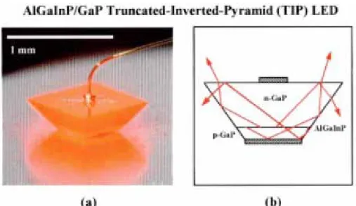
Fig. 2-1 Band diagram of active region of LEDs
Fig. 2-3 Definition of the escape cone by the critical angle θc.
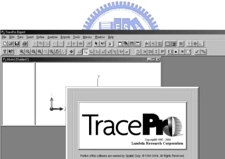
Fig. 2-4 Image of Tracepro software
Θc
90° na
Chapter 3
V-shape sapphire facet reflector LEDs
3.1 Monte-Carlo ray-tracing calculations
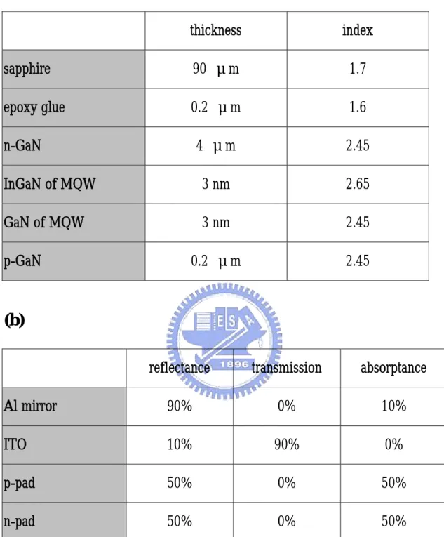
In order to investigate the fundamental of enhancement of light output with different etching time of V-shape sapphire facet reflector LEDs, we used a commercial ray-tracing software employing the Monte-Carlo algorithm for forward ray-tracing, various outputs including efficiency value, spatial distributions of radiometric and photometric data. Shape and size of the solid model for the ray-tracing calculation was shown in the Table 3-1(a), (b) and Fig. 3-1(a), (b), (c). Table 3-1(a) shown the material variable of the models ,and Table 3-1(b) shown the surface variable of the models. The wavelength and temperature in my simulation were 450 nm and 300K, respectively. Fig. 3-1(a) shown the structure of the simulated models, and Fig. 3-1(b) shown the models in the TracePro software. Because the thickness of the sapphire layer was thicker than others, the epitaxial layer was not clear in Fig. 3-1(b). Fig. 3-1(c) was a sketch of the pattern on the sapphire substrate. The circles in the figure represent holes in my models. The arrangement of the holes were hexagonal matrix ,and the distance of the center of the hole was 7 μm. The simulated models were exactly the same as the SEM images and microscopic measurements of the geometry of CWE-PSS LEDs afterward.
The solid model was built up as a combination of simple solid objects, each semiconductor layer adjacent to the other. According to the recombination process [25], light rays were generated in the active layer with a uniform random distribution. Monochromatic radiation representing the peak wavelength of the measured spectral emission (450 nm) was used in the simulation.
result of etching 120sec was better than flat, outstandingly.
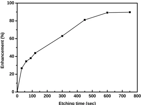
The comparison of overall light extraction efficiency was plotted and shown in the Fig. 3-2(c). According to this calculation, the light extraction efficiency is dramatically enhanced with the increasing of sapphire etching time. For this result, we select etching time 120sec to fabricate V-shape sapphire facet reflector LEDs.
Fig. 3-3 show the further simulated results with long etching time from 0 to 750 sec. The output power is increase with the raise of etching time and gradually converges. This shows that we can try to fabricate patterned sapphire substrate with longer etching time in the future.
3.2 Fabrication of V-shape sapphire facet reflector LEDs 3.2.1 Process procedure
The GaN-based LEDs used in this study were grown using a low-pressure metal-organic chemical vapor deposition (Aixtron 2600G) system onto the C-face (0001) 2”-diamerter sapphire substrate. The LED layer-structure comprised a 30-nm-thick GaN nucleation layer, a 2-µm-thick undoped GaN layer, a 2-µm-thick Si-doped n-type GaN cladding layer, an un-intentionally doped active region with five periods of InGaN/GaN multiple quantum wells (MQWs), and a 0.2-µm-thick Mg-doped p-type GaN cladding layer.
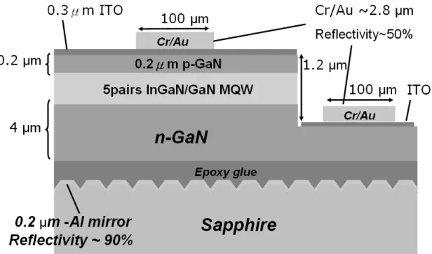
Fig. 3-4(a)~(e) shows the fabrication steps of GaN-based LEDs with an Al-deposited V-shape sapphire facet reflector by double transferred and laser-lift-off (LLO) techniques. The grown wafer was patterned with square mesas 350 x 350 µm2 in size by a standard
photolithographic process and was partially etched until the exposure of n-GaN to define the emitting area and n-electrode; a 300-nm-thick ITO was deposited as the transparent conductive layer and Cr/Au were then deposited as n and p electrodes and was alloyed at 200
oC in N
2 atmosphere for 5 minutes [Fig. 3-4(a)]. The processed wafer was then brought into
1.6 at 470 nm) at an operating temperature of 80 oC [Fig. 3-4(b)]. The bonded structure was then subjected to the LLO process [Fig. 3-4(c)]. A KrF excimer laser at a wavelength of 248 nm with a pulse width of 25 ns was used to remove the sapphire substrate. The laser with a beam size of 1.2 mm x 1.2 mm was incident from the backside of the sapphire substrate onto the sapphire/GaN interface to decompose GaN into Ga and N2. In this process, the beam size
of KrF laser was larger than that of the size of the LEDs. Therefore, the laser irradiation on the interface of sapphire and GaN was uniform. The GaN thin-film was again brought into contact with the Al-deposited V-shaped sapphire facet reflector using epoxy glue at an operating temperature of 80 oC [Fig. 3-4(d)]. The fabrication of Al-deposited V-shaped sapphire facet reflector was illustrated as following: the SiO2 film with hole-patterns of a
diameter of 3 µm was deposited onto the sapphire substrate by plasma-enhanced chemical vapor deposition (PECVD) and defined by standard photolithography to serve as the wet etching mask. The sapphire substrate was then wet etching using an H3PO4-based solution
with an etching time of 120s and etching temperature of 250 oC. The sapphire wet-etching rate is about 0.8 µm/minute in this study and can be related to the H3PO4 composition and
etching temperature [9]. A sapphire substrate with V-shape facet patterns was formed after the chemical wet etching process. A 200-nm-thick Al metal with a reflectivity of about 90 % was then deposited on the top of the V-shaped sapphire substrate by e-beam evaporation. After the re-bonding process, the GaAs carrier was removed using a NH4OH-based solution [Fig.
3-4(e)]. Thus GaN-based LEDs with high reflectivity V-shape sapphire facet reflector could be realized by adopting this what we called the double transferred technique since the LED epitaxy was firstly transferred into a sacrifice GaAs substrate and LLO process, re-transferred into a host sapphire substrate with Al-deposited V-shape reflectors. Fig. 3-5 shown the detail size of the V-shape sapphire facet reflector LEDs. The conventional LEDs have the same structure except sapphire substrate. It should also be noted that although the thermal
conductivity of epoxy glue (~0.32 W/ mK) here we used for the attaching material is lower than that of the sapphire substrate (~23W/ mK), the ability of heat dissipation of this novel structure will not be degraded due to the thin thickness of epoxy glue. By specifically adjusting the bonding pressure, the thickness of epoxy glue could be well controlled and a thickness as thin as 0.2 µm could be achieved. Therefore, the heat that generated while operating the LED can easily penetrate through the thin epoxy glue in spite of the relative low thermal conductivity, indicating that it will not exist any disadvantage in terms of heat dissipation, as comparing to the ordinary LED. The reference LED sample with exactly the same procedure, but without wet etching sapphire substrate process, was also prepared for comparison.
3.2.2 SEM images of patterned sapphire substrates
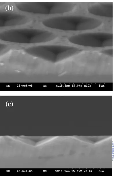
Fig. 3-6 shows scanning electron micrograph (SEM) images of the wet etched sapphire substrate. According to Fig. 3-6, the etched V-shape facet of an (0001)-oriented sapphire substrate has the R-plane {1-102} facet, and the angle against {0001} C-axis is about 57o.
This large etching slope is useful for providing appropriate slant surfaces, which are helpful to the light extraction, according to the calculated results based on the Monte-Carlo ray tracing simulation [11]. Besides, this high slope facet using chemical wet etching is difficult to achieve by using other methods, such as the ICP dry etching, and the smooth crystal facet of R-plane is quite suitable for the subsequent deposition of the metal layer serving as a reflector. Thus, a high slope and reflectivity V-shape sapphire reflector for increasing the light extraction efficiency of LEDs can be realized by adopting the sapphire wet etching process.
3.3 Characteristics of V-shape sapphire facet reflector LEDs
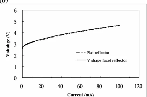
characteristics of flat and V-shape Al-deposited sapphire reflector LEDs as a function of forward driving current. The L-I-V characteristics were measured with an on-wafer testing configuration, consisting of the Si detector mounted directly above the LED and the driving current being applied through the probes. It means that the power measurement is a relative axial output from the top surface of the chip. As can be seen in Fig. 3-7(a), the light output power of both structures increased continuously as the driving current was increased from 0 to 100 mA. The light output power of the V-shape sapphire facet reflector LEDs has higher output power of about 40% compared to the flat Al-deposited sapphire reflector LEDs at an injection current of 20 mA, i.e., a significant improvement attributed to the V-shape sapphire facet reflector to effectively reflect the emission light toward to the chip surface. In Fig. 3-7(b), about 3.3 V of forward voltages was measured on both devices at the injection current of 20 mA and no significant difference of the I-V curves were observed under the measurement condition of the driving current up to 100 mA, indicating that a feasible process for high brightness GaN-based LEDs was achieved without electrical damage.
In order to realize the enhancement mechanism of output power by adopting the V-shape sapphire facet reflector, the top view light-emission of LEDs were observed by charge-coupled device (CCD) and the obtained images are shown in Fig. 3-8 The photograph of the GaN-based V-shape Al-deposited sapphire reflector LED without current driving is shown in Fig. 3-8(a). According to this figure, a V-shape sapphire facet reflector is successfully attached to the LED epitaxy using double transferred technique. Fig. 3-8(b) shows the light-emission image of the enlarged photograph of area A in Fig. 3-8(a) under a driving current of 20 mA. In this figure, the emitting light from the LED mesa edge is redirected toward to the axial direction by the V-shape sapphire facet reflector, thus higher intensity was observed on the individual V-shape pattern than that on other regions, indicating that employing the V-shape sapphire facet reflector has the superior benefit for improving the
light extraction efficiency by effectively redirecting the guided light in side the LED chip toward to the top escape cone.
(a)
thickness
index
sapphire
90 μm
1.7
epoxy glue
0.2 μm
1.6
n-GaN
4 μm
2.45
InGaN of MQW
3 nm
2.65
GaN of MQW
3 nm
2.45
p-GaN
0.2 μm
2.45
(b)
reflectance
transmission
absorptance
Al mirror
90%
0%
10%
ITO
10%
90%
0%
p-pad
50%
0%
50%
n-pad
50%
0%
50%
Table 3-1 (a) shown the material variables of the simulated models. And, (b) shown the surface variables of the models.
(a)
(C)
Fig. 3-1 (a) shown the structure of the simulated models. (b) shown the models in the TracePro software. (c) is a sketch of the pattern on the sapphire substrate.
(b)
(c)
0 30 60 90 120 0 10 20 30 40 50 En hancement (% )Etching time (sec)
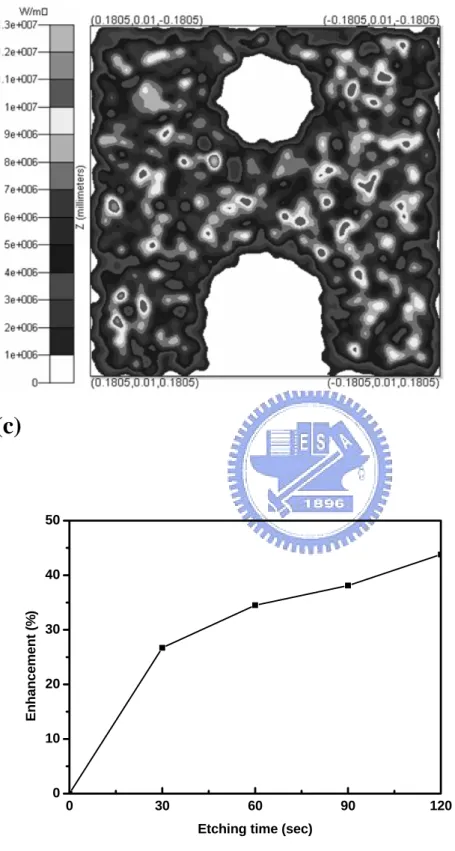
Fig. 3-2 The Monte-Carlo ray-tracing calculated results of radiation patterns of the calculated enhancement on the light extraction efficiency with the increasing of sapphire etching time. (a) and (b) shown the irradiance maps of flat and etching 120sec structures. (c) shown the comparison of overall light extraction efficiency.
0 100 200 300 400 500 600 700 800 0 20 40 60 80 100 Enhancemen t (% )
Etching time (sec)
Fig. 3-3 show the simulated results with long etching time from 0 to 750 sec.
Fig. 3-4 Schematic of fabrication steps for GaN LEDs with sapphire facet mirror adopting double-transferred technique.
Fig. 3-5 shown the detail size of the V-shape sapphire facet reflector LEDs. The conventional LEDs have the same structure except sapphire substrate.
Fig. 3-6 SEM images of the wet etching sapphire substrate with R-plane of {1-102}. (a) top view , (b) and (c) cross-section side view images.
(a)
(c)
(b)
(b)
Fig. 3-7 (a)The output power (L-I curve) and (b) current-voltage (I-V curve) characteristics of flat and V-shape Al-deposited sapphire reflector LEDs as a function of forward driving current.
Fig. 3-8 The top view light-emission images. (a) Plan-view photograph of the GaN-based V-shape Al-deposited sapphire reflector LED. (b) The light-emission image of the enlarged photograph of area A in Fig. 3-8(a) under a driving current of 20 mA.
Chapter 4
Chemical wet-etched patterned sapphire substrate (CWE-PSS)
LED
4.1 Fabrication of CWE-PSS LED 4.1.1 Process procedure
The GaN-based LEDs used in this study were grown using a low-pressure metal-organic chemical vapor deposition (Aixtron 2600G) system onto the C-face (0001) 2”-diamerter chemical wet-etched patterned sapphire substrates. The LED layer-structure comprised a 30-nm-thick GaN nucleation layer, a 2-µm-thick undoped GaN layer, a 2-µm-thick Si-doped n-type GaN cladding layer, an un-intentionally doped active region of 450-nm emitting wavelength with five periods of InGaN/GaN multiple quantum wells (MQWs), and a 0.2-µm-thick Mg-doped p-type GaN cladding layer. The grown wafer was patterned with square mesas of 350 x 350 µm2 in size by a standard photolithographic process and was
partially etched until the exposure of n-GaN to define the emitting area and n-electrode; a 300-nm-thick ITO was deposited as the transparent conductive layer and Cr/Au was then deposited as n and p electrodes and was alloyed at 200 oC in N2 atmosphere for 5 minutes. Fig.
4-1 shows the process chart of the GaN-based LED grown on CWE-PSS.
For fabricating the CWE-PSS, the SiO2 film with hole-patterns of 3-µm-diameter and
3-µm-spacing was deposited onto the sapphire substrate by plasma-enhanced chemical vapor deposition (PECVD) to serve as the wet etching mask. The sapphire substrate was then wet etched using an H3PO4-based solution at an etching temperature of 300 oC. The sapphire
wet-etching rate was about 1 µm/minute in this study and can be related to the H3PO4
4.1.2 SEM images of patterned sapphire substrates
Fig. 4-2 (a) and (b) show the SEM images of the pattern sapphire substrate of the etching time of 90s and 120s, respectively. In Fig. 4-2(a), the crystallography-etched pattern of an (0001)-oriented sapphire substrate has a flat-surface of {0001} C-plane with triangle-shape in the center. Surrounding the triangle-shape C-plane are three facets of {1-102} R-plane with angle of 57° against the [0001] C-axis. However, due to the relative fast etching rate of C-plane than that of R-plane, the triangle-shape flat-surface of {0001} C-plane in the pattern center finally vanishes with the increasing of the etching time. As shown in Fig. 4-2(b), the {0001} C-plane is absent and only {1-102} R-plane is observed on the CWE-PSS with the etching time of 120s. Fig. 4-2(c) shows the evolution of CWE-PSS with the increasing of sapphire etching time. It should be noted that the diameter of the sapphire pattern also increases with the increasing of etching time due to the side-etching effect; however, the period of the sapphire pattern keeps the same as 6-µm. Additionally, the high slope (57°) crystallography-etched facet of CWE-PSS is hard to fabricate by dry etching and it has been demonstrated in our previous work that this inclined facet has the superior capability for improving light extraction efficiency [15].
4.2 Characteristics of CWE-PSS LED 4.2.1 The HR-XRDs of the CWE-PSS LEDs
In order to investigate the film quality of CWE-PSS LEDs, the epitaxial wafers were analyzed by the high-resolution X-ray rocking curves (Bede D1 HR-XRD). Fig. 4-3 shows the HR-XRDs of the (0002) reflection of the CWE-PSS LEDs.
The measurements over wide range (-4000~3000 arcsec) and narrow range (-100~100 arcsec) are shown in Fig. 4-3(a) and Fig. 4-3(b), respectively. In Fig. 4-3(a), the same location of satellite-peaks over the wide measurement range for the conventional (sapphire etching
time of 0s) and all CWE-PSS LEDs indicates that the LED composition and growth rate were not associated with the CWE-PSS. However, according to Fig. 4-3(b), the full-width at half-maximum (FWHM) of main peak was about 40 arcsec for the conventional LED and was about 30 arcsec for all CWE-PSS LEDs. An obvious broad shoulder was observed near the main peak for the conventional LED. It suggested that the better crystalline quality was achieved on CWE-PSS LEDs and was consistent with the well accepted concept that the growth on the pattern sapphire substrate exhibited a considerable improvement on internal quantum efficiency by reducing the threading dislocation density, no matter on dry etching or chemical wet etching patterned sapphire substrates [16-22].
4.2.2 L-I measurement and external quantum efficiency
For comparing the LED performances with different crystallography-etched facet patterns, the sapphire substrates of etching times of 0s, 30s, 60s, 90s, and 120s, were employed into this report. All of these CWE-PSSs were then grown and processed at the same time, eliminating any artificial issue during LED fabrication. The LED chips were packaged into TO-18 without epoxy resin for the subsequent measurement. The typical light-current-voltage (L-I-V) measurements were performed using a high current measure unit (KEITHLEY 240). The light output power of the LEDs was measured using an integrated sphere with a calibrated power meter.
Fig. 4-4(a) shows the measurement results of room temperature output power (L-I curve) of conventional and CWE-PSS LEDs as a function of the forward-bias current. In this figure, all the CWE-PSS LEDs demonstrate a significant improvement on output power as comparing to the conventional LED under our measurement condition up to 200 mA. The enhanced factor of output power of CWE-PSS LEDs compared to the conventional LED at a driving current of 20 mA is shown in Fig. 4-4(b). According to this figure, the optimized CWE-PSS condition was achieved on the etching time of 90s, corresponding to an enhanced
factor of output power of 1.4. Fig. 4-4(c) shows the external quantum efficiency (EQE) of the conventional and CWE-PSS LEDs with the forward injection currents up to 100 mA. It was found that the EQE of the CWE-PSS LED with etching time of 90s reached a maximum value of about 25 % at an injection current of 5 mA and then decreased significantly with a further increase in the forward bias current. Nearly the same trend was also obtained for the conventional LED sample except for a lower EQE value of 17.8 %. The degradation at the higher current might be due to reflow of injection carriers and the joule heating effect. It should be pointed out that even though the CWE-PSS LEDs performance in absolute terms of external quantum efficiency does not exceed state-of-the-art devices using other approaches, comparison is being made on the overall intensity enhancement using the CWE-PSS scheme.
4.2.3 Monte-Carlo ray-tracing calculations
In order to investigate the fundamental of enhancement of light output with different etching time of CWE-PSS LEDs, we used a commercial ray-tracing software employing the Monte-Carlo algorithm for forward ray-tracing, various outputs including efficiency value, spatial distributions of radiometric and photometric data. Shape and size of the solid model for the ray-tracing calculation was determined and exactly the same as the SEM images and microscopic measurements of the geometry of CWE-PSS LEDs, as shown in Fig. 4-1 and Fig. 4-2. The solid model was built up as a combination of simple solid objects, each semiconductor layer adjacent to the other. According to the recombination process, light rays were generated in the active layer with a uniform random distribution. Monochromatic radiation representing the peak wavelength of the measured spectral emission (450 nm) was used in the simulation.
Fig. 4-5 shows the calculated radiation patterns of (a) CWE-PSS LEDs with etching time of 30s (b) the conventional. A stronger axial radiation on the CWE-PSS LED than that of the conventional LED was observed in this figure. The same epitaxial models were also built on
the other CWE-PSS LEDs with the etching time of sapphire substrate of 60s, 90s, and 120s. The comparison of overall light extraction efficiency was plotted and shown in the Fig. 4-5(c). According to this calculation, the light extraction efficiency is dramatically enhanced with the increasing of sapphire etching time and. even more than twice large of magnitude of light output was observed on the CWE-PSS LED with the etching time of 120s. Therefore, the crystallography-etched patterns that evolving with the increasing of etching time of sapphire substrate affect the light extraction efficiency profoundly. With the increasing of the etching time, the triangle-shape flat-surface of {0001} C-plane in the pattern center finally vanishes, due to its relative fast etching rate than that of {1-102} R-plane. The sustained {1-102} R-plane has an inclined crystallography-etched facet with a high slope as large as 57o, adding
the opportunity of the guided light to meet the escape cone on the top of chip surface.
Fig. 4-6 is a simple schematic ray-tracing of the CWE-PSS LEDs with the increasing of sapphire etching time. In the case of the CWE-PSS LED with the large {0001} C-plane pattern, i.e., a short period of sapphire etching time, the light emitting from the LED active region (MQW) was much easier to be guided inside the LED chip, as compared to that of the longer period of etching time, corresponding to the larger surface of high-slope crystallography-etched facets of {1-102} R-plane. As shown in Fig. 4-6, more guided light can be extracted from the LED top surface, enhancing the total light output power. This is the reason why in Fig. 4-5(b), we can observe the strong illumines in the axial direction on the CWE-PSS LED.
As comparing the ray-tracing calculation and real device measurement, an inconsistent behavior on the sapphire etching time of 120s was observed due to the un-optimization of epitaxial condition by MOCVD. The cross-section side-view SEM images of CWE-PSS LEDs with different etching time of (a) 30s, (b) 60s, (c) 90s, and (d) 120s were shown in Fig. 4-7. The crystallography-etched sapphire patterns can be buried completely by the GaN
epitaxy in all CWE-PSS LEDs, except for the sample of the etching time of 120s. According to the ray-tracing calculation, the light extraction efficiency was significantly improved with the increasing of sapphire etching time and could be contributed to the high-slope crystallography-etched facet of {1-102} R-plane. However, the large inclined crystallography-etched surface also indicates the deep depth of the sapphire pattern, and it also takes more effort for adjusting the growth condition to obtain a high-quality GaN film. As shown in Fig. 4-7 (d), a void locating inside the sapphire pattern can be observed due to the relative difficult for MOCVD to grow on this deep and inclined crystallography-etched facet pattern. Therefore, in the Fig. 4-4(b), a drop of light extraction efficiency was observed on the CWE-PSS LED of sapphire etching time of 120s. Beside, we do not consider the surface morphology while building the ray-tracing calculation model. Thus, another conflict on the absolute term of enhancement of the light output was observed, as comparing to Fig. 4-4(b) and Fig. 4-5(c). As can be seen in Fig. 4-7, the surface of LED chip is quite rough, and that is not taken into account on the ray-tracing calculation. By ignoring these epitaxial issues as mentioned above, both the ray-tracing calculation and real device measurement depict the same trend on the enhancement of light extraction efficiency, indicating the modeling of LED chip by ray-tracing calculation can be a powerful tool in predicting the efficiency of LED optics designs.
Fig. 4-8(a) and (b) show the simulated results with long etching time from 0 to 750 sec. In this figure, the enhanced factor is increase with the raise of etching time and gradually converges. In the future, if we can improve epitaxial processes, we can employ longer etching time PSS and enhance extraction efficiency further.
4.2.4 Reliability test of CWE-PSS LEDs
In Fig. 4-9, A reliability test was performed on the conventional and CWE-PSS LEDs under a driving current of 55 mA at 55 oC. Referring to previous data, the decay of the output
power at 55 mA, 55 °C after 96 hours is equal to the results at 20mA, 25 °C after 1000 hours. the EL intensity to the initial EL intensity is shown as a function of the aging time. According to this figure, all the life-testing samples exhibit the same degradation trend. However, all the CWE-PSS LEDs present a gradual degradation in the EL intensity under our measurement condition up to 600 hours. In general, the EL intensity of conventional and CWE-PSS LEDs were decayed by about 20% and 10%, respectively; indicating the improvement on the epitaxial quality could be achieved via grown on the CWE-PSS scheme.
Fig. 4-1 The schematic drawing of process charts with chemical wet-etched patterned sapphire substrate (CWE-PSS).
(a)
(a) Sapphire (c) n-GaN p-GaN MQW Patterned Sapphire (d) p-GaN Patterned Sapphire n-GaN MQW Patterned Sapphire (b) (f) p-GaN Patterned Sapphire n-GaN MQW Cr/Au (e) 300nm ITO p-GaN Patterned Sapphire n-GaN MQW(b)
(C)
Fig. 4-2 (a) and (b) show the SEM images of the CWE-PSS of the etching time of 90s and 120s, respectively. (c) A top-view drawing depicts the evolution of CWE-PSS with the increasing of etching time.
-4000 -2000 0 2000 In te ns ity (a .u.) Arcsec 0s 30s 60s 90s 120s -150 -100 -50 0 50 100 150 Intensi ty (a .u .) Arcsec 0s 30s 60s 90s 120s
Fig. 4-3 The high-resolution X-ray rocking curves (Bede D1 HR-XRD). Measurements over (a) wide range (-4000~3000 arcsec) and (b) narrow range (-100~100 arcsec).
(a)
(a)
(b)
1.0
1.1
1.2
1.3
1.4
1.5
0
30
60
90
120
150
Etching Time (s)
E
nha
nc
em
ent
(c)
Fig. 4-4 (a) The measurement results of room-temperature output power (L-I curves) of the conventional and CWE-PSS LEDs (b) the enhancement factor on output power while comparing the CWE-PSS LEDs to the conventional LED under the driving current of 20 mA, and (c) the external quantum efficiency (EQE) of the conventional and CWE-PSS LEDs with the forward injection currents up to 100 mA.
(b)
(c)
Fig. 4-5 The Monte-Carlo ray-tracing calculated results of radiation patterns of (a) the conventional (b) CWE-PSS LEDs with etching time of 30s. (c) The calculated enhancement on the light extraction efficiency with the increasing of sapphire etching time.
Fig. 4-6 A schematic ray-tracing of the CWE-PSS LEDs with the increasing of sapphire etching time.
Fig. 4-7 The cross-section side-view SEM images of CWE-PSS LEDs with different etching time of (a) 30s, (b) 60s, (c) 90s, and (d) 120s.
0 100 200 300 400 500 600 700 800 1.0 1.2 1.4 1.6 1.8 2.0 2.2 2.4 E nha nce d fa ct or
Etching time (sec)
Fig. 4-8 show the simulated results with long etching time from 0 to 750 sec.
0 100 200 300 400 500 600 0.0 0.2 0.4 0.6 0.8 1.0 1.2 E L Intensity V a riation
Aging time (hour) 0 sec
30 sec 60 sec 90 sec 120 sec
Fig. 4-9 Reliability test of the conventional and CWE-PSS LEDs under stress condition of 55 oC and 50 mA.
Chapter 5
Conclusions and future work
5.1 Conclusions
In summary, we fabricated two kinds of LEDs with novel structures. In the first structure, high light-extraction-efficiency GaN-based LEDs employing an Al-deposited, R-plane of {1-102} with 57o against C-axis and V-shape sapphire facet reflector were successfully fabricated. A Monte-Carlo ray-tracing calculation was employed to design the geometric patterns of these V-shape sapphire facet reflector LEDs. The output power is increased by approximately 40% on this novel structure compared with the standard one with a flat reflector at an injection current of 20 mA, and with an normal forward voltage of about 3.3 V. The improvement is attributable to the geometrical shape of sapphire facet reflector that enhances the light extraction efficiency by redirecting the guided light toward to the top exit cone of the LED surface.
And, in the second structure, the characteristics of GaN-based LEDs grown on patterned sapphire substrate fabricated by the chemical wet etching were specifically analyzed. By chemical wet etching, the sapphire substrate exhibited a particular crystallography-etched facet of {1-102} R-plane with an inclined slope as large as 57o, demonstrating a significant
enhancement of the light extraction efficiency. A Monte-Carlo ray-tracing calculation was also employed to further investigate and design the geometric patterns of this novel CWE-PSS LEDs, and a consistent agreement was observed between theoretical calculation and the real device measurement. Moreover, an improvement of epitaxial quality was also observed on CWE-PSS LEDs, according to the measurement results of the high-resolution X-ray rocking curves (HR-XRDs) and device reliability testing. Therefore, by using this novel
CWE-PSS scheme, an overall enhancement of 40 % on the external quantum efficiency can be achieved, that is not only due to the improvement of the internal quantum efficiency upon reducing the dislocation density, but also contributed to the geometrical shape of the inclined crystallography-etched facets that can efficiently scatter the guided light to enter the escape cone.
5.2 Future work
In this report,we discovered that the epitaxial layer grown on patterned sapphire substrate was provided with better quality. Besides, PSS structure can redirect the light emitted from active layer toward to the exit cone of the LED surface as well as enhance extraction efficiency.
In the future, we will try to fabricate double-side patterned substrate. Using photolithography and H3PO4-based solution at an etching temperature of 300 oC etch the back
side of PSS. Al metal with a reflectivity of about 90 % was then deposited on that surface. Subsequently, we will grow epitaxial layer and carry out othe processes. Furthermore, we will try to combine two structures, V-shape sapphire facet reflector LED and CWE-PSS LED, with other structures, for instance, p-GaN surface roughening process or photonic crystal(Fig. 5-1).
Reference
[1] S. Nakamura, G. Fasol, “The Blue Laser Diode,” Springer, New York, 1997.
[2] S. Nakamura, M. Senoh, N. Iwasa, and S. Nagahama, “High-brightness InGaN blue, green and yellow light-emitting diodes with quantum well structures,” Jpn. J. Appl. Phys., vol. 34, p. L797, 1995.
[3] H. Morkoc, S. Strite, G.B. Gao, M.E. Lin, B. Sverdlov, M. Burns, “Large-band-gap SIC, III-V nitride, and II-VI ZnSe-based semiconductor device technologies,” J. Appl. Phys. vol.76, pp1363–1398, 1994.
[4] M. Koike, N. Shibata, H. Kato, and Y. Takahashi, “Development of High Efficiency GaN-Based Multiquantum-Well Light-Emitting Diodes and Their Applications,” IEEE JOURNAL ON SELECTED TOPICS IN QUANTUM ELECTRONICS, vol. 8, pp 271-277, 2002.
[5] S. H. Lydecker, K. F. Leadford, C. A. Ooyen, “Lighting Industry Acceptance of Solid State Lighting,” Proc. of SPIE, vol. 5187, pp 22-33, 2004.
[6] Jianghong Jiao, Ben Wang, “Etendue Concerns for Automotive Headlamps Using White LEDs, Proc. of SPIE, vol. 5187, pp 234-242, 2004.
[7] S.D. Lester, F.A. Ponce, M.G. Craford and D.A.Steigerwald, “High dislocation densities in high efficiency GaN-based light-emitting diodes ”, Appl. Phys. Lett. vol.66, pp1249-1251, 1995.
[8] M. Broditsky and E. Yablonovitch, “Light-emitting-diode extraction efficiency,” Proc. Spie, vol. 3002, pp119-122, 1997.
[9] M.R. Krames, M. Ochiai-Holcomb, G. E. Höfler, C. Carter-Coman, E. I. Chen, I. –H. Tan, P. Grillot, N. F. Gardner, H. F. Gardner, H.C. Chui, J. -W. Huang, S. A. Stockman, F. A. Kish, and M. G. Craford, “High-power truncated-inverted-pyramid (AlxGa1–x)0.5In0.5P/GaP
light-emitting diodes exhibiting >50 external quantum efficiency,” Appl. Phys. Lett. vol. 75, pp2365-2367, 1999.
[10] C. Huh, K.-S. Lee, E.-J. Kang, and S.-J. Park, “Improved light-outputand electrical performance of InGaN-based light-emitting diode by microroughening of the p-GaN surface,” J. Appl. Phys., vol. 93, pp.9383–9383, 2003.
[11] S. J. Chang, L. W. Wu, Y. K. Su, Y. P. Hsu, W. C. Lai, J. M. Tsai, J. K. Sheu, and C. T. Lee, “Nitride-based LEDs with 800 C grown p-AlInGaN-GaN double-cap layers,” IEEE Photon. Technol. Lett., vol.16, no. 6, pp. 1447–1449, Jun. 2004.
[12] Y. Gao, T. Fujii, R. Sharma, K. Fujito, S. P. Denbaars, S. Nakamura, and
E. L. Hu, “Roughening hexagonal surface morphology on laser lift-off (LLO) N-face GaN with simple photo-enhanced chemical wet etching,” Jpn. J. Appl. Phys., vol. 43, pp. 637–637, 2004.
extraction efficiency of GaN-based light-emitting diodes via surface roughening,” Appl. Phys. Lett., vol. 84, pp. 855–855, 2004.
[14] T. N. Oder, K. H. Kim, J. Y. Lin, and H. X. Jiang, “III-nitride blue and ultraviolet photonic crystal light emitting diodes,” Appl. Phys. Lett., vol. 84, pp. 466–468, 2004.
[15] C. C. Kao, H. C. Kuo, H. W. Huang, J. T. Chu, Y. C. Peng, Y. L. Hsieh, C. Y. Luo, and S. C. Wang, “Light-output enhancement in a nitride-based light-emitting diode with 22o undercut sidewalls,” IEEE Photon. Technol. Lett. vol. 17, pp 19-21, 2005.
[16] H. W. Huang, C. C. Kao, J. T. Chu, H. C. Kuo, S. C. Wang, and C. C. Yu, “Improvement of InGaN–GaN Light-Emitting Diode Performance With a Nano-Roughened p-GaN Surface,” IEEE Photon. Technol. Lett. vol. 17, pp 983-985, 2005.
[17] Y. J. Lee, H. C. Kuo, S. C. Wang, T. C. Hsu, M. H. Hsieh, M. J. Jou, and B. J. Lee “Increasing the extraction efficiency of AlGaInP LEDs via n-side surface roughening ”, IEEE Photonic Technology Letter, vol. 17, pp2289-2291, 2005.
[18] Y. J. Lee, H. C. Tseng, H. C. Kuo, S. C. Wang, C. W. Chang, T. C. Hsu, Y. L. Yang, M. H. Hsieh, M. J. Jou, and B. J. Lee, “Improvement in Light-Output Efficiency of AlGaInP LEDs Fabricated on Stripe Patterned Epitaxy”, IEEE Photonic Technology Letter, vol. 17, pp2532-2534, 2005.
[19] Y. J. Lee, T.C. Lu, H.C. Kuo, S.C. Wang, M. J. Liou, C.W. Chang, T. C. Hsu, M. H. Hsieh, M. J. Jou, and B. J. Lee, “AlGaInP LEDs with Stripe Patterned Omni-Directional Reflector”, Jpn. J. Appl. Phys., vol. 45, pp643-645, 2006.
[20] Y. J. Lee, T.C. Lu, H.C. Kuo, S.C. Wang, M. J. Liou, C.W. Chang, T. C. Hsu, M. H. Hsieh, M. J. Jou, and B. J. Lee, “High brightness AlGaInP-based light emitting diodes by adopting the stripe-patterned omni-directional reflector”, Semicond. Sci. Technol. vol.21, pp.184–189, 2006.
[21] Y. J. Lee, J.M. Hwang, T. C. Hsu, M. H. Hsieh, M. J. Jou, B. J. Lee, T.C. Lu, H.C.Kuo, and S.C. Wang, “GaN-based LEDs with Al-Deposited V-Shape Sapphire Facet Mirror,” IEEE Photon. Technol. Lett, accepted for publication, vol.18, 2006.
[22] K. Tadatomo, H. Okagawa, Y. Ohuchi, T. Tsunekawa, Y. Imada, M. Kato, T. Taguchi, “ High Output Power InGaN Ultraviolet Light Emitting Diodes Fabricated on Patterned Substrates Using Metalorganic Vapor Phase Epitaxy,” Jpn. J. Appl. Phys. vol. 40, L583–L585, 2001.
[23] M. Yamada, T. Mitani, Y. Narukawa, S. Shioji, I. Niki, S. Sonobe, K. Deguchi, M. Sano, T. Mukai, “InGaN-Based Near-Ultraviolet and Blue-Light-Emitting Diodes with High External Quantum Efficiency Using a Patterned Sapphire Substrate and a Mesh Electrode,” Jpn. J. Appl. Phys. vol. 41, L1431–L1433, 2002.
[24] D.S. Wuu, W.K. Wang, W.C. Shih, R.H. Horng, C.E. Lee, W.Y. Lin, J.S. Fang, “Enhanced Output Power of Near-Ultraviolet InGaN–GaN LEDs Grown on Patterned
Sapphire Substrates,” IEEE Photon. Technol. Lett. vol.17, pp. 288– 290, 2005
LEDs Grown on Grooved Sapphire Substrates,” IEEE Photon. Technol. Lett. vol.17, pp. 1812– 1814, 2005.
[26] Y. J. Lee, T. C. Hsu, H.C. Kuo, S.C. Wang, Y.L. Yang, S.N. Yen, Y.T. Chu, Y.J. Shen, M.H. Hsieh, M.J. Jou, B.J. Lee, “Improvement in light-output efficiency of Near-Ultraviolet InGaN–GaN LEDs Fabricated on Stripe Patterned Sapphire Substrates”, Material Science and Engineering: B, vol. 122, pp184-187, 2005.
[27] Y. J. Lee, J.M.Hwang, T. C. Hsu, M. H. Hsieh, M. J. Jou, B. J. Lee, T.C. Lu, H.C. Kuo, and S.C. Wang, “Enhancing Output Power of GaN-based LEDs Grown on Chemical Wet Etching Patterned Sapphire Substrate,” revised for publication, IEEE Photonic Technology Letter, 2006.
[28] J. Wang, L. W. Guo, H. Q. Jia, Z. G. Xing, Y. Wang, H. Chen and J. M. Zhou, “ Origin of Selective Growth of GaN on Maskless V-Grooved Sapphire Substrate by Metalorganic Chemical Vapor Deposition,” Jpn. J. Appl. Phys., vol. 44, pp. L982-L984, 2005