Annealing dynamics of nitrogen-implanted GaAs films investigated by current–voltage
and deep-level transient spectroscopy
J. F. Chen, J. S. Wang, M. M. Huang, and N. C. Chen
Citation: Applied Physics Letters 76, 2283 (2000); doi: 10.1063/1.126322
View online: http://dx.doi.org/10.1063/1.126322
View Table of Contents: http://scitation.aip.org/content/aip/journal/apl/76/16?ver=pdfcov Published by the AIP Publishing
Articles you may be interested in
Effects of thermal annealing on deep-level defects and minority-carrier electron diffusion length in Be-doped InGaAsN
J. Appl. Phys. 97, 073702 (2005); 10.1063/1.1871334
Observed trapping of minority-carrier electrons in p -type GaAsN during deep-level transient spectroscopy measurement
Appl. Phys. Lett. 86, 072109 (2005); 10.1063/1.1865328
Deep nitrogen implantation for GaAs microstructuring using pulsed electrochemical etching J. Appl. Phys. 92, 2923 (2002); 10.1063/1.1498886
Determination of energy levels of surface states in GaAs metal–semiconductor field-effect transistor using deep-level transient spectroscopy
Appl. Phys. Lett. 74, 1108 (1999); 10.1063/1.123458
Structures and defects in arsenic-ion-implanted GaAs films annealed at high temperatures J. Appl. Phys. 81, 7295 (1997); 10.1063/1.365327
This article is copyrighted as indicated in the article. Reuse of AIP content is subject to the terms at: http://scitation.aip.org/termsconditions. Downloaded to IP: 140.113.38.11 On: Thu, 01 May 2014 07:53:08
Annealing dynamics of nitrogen-implanted GaAs films investigated
by current–voltage and deep-level transient spectroscopy
J. F. Chen, J. S. Wang, M. M. Huang, and N. C. Chen
Department of Electrophysics, National Chiao Tung University, Hsinchu 30050, Taiwan, Republic of China 共Received 16 August 1999; accepted for publication 24 February 2000兲
We present electrical data to show that, after nitrogen implantation, GaAs films become resistive after high-temperature annealing. The activation energies of the resistance are determined to be 0.34, 0.59, and 0.71 eV after annealing at 500, 700, and 950 °C, respectively. The increase in the activation energy with increasing annealing temperature can be explained by the results of traps detected in deep-level transient spectroscopy, where two traps at 0.32 and 0.70 eV are observed in the samples after annealing. The intensity of the trap at 0.32 eV is found to reduce by annealing. By comparing to the result of the x-ray diffraction, we suspect that this trap is related to the lattice-expansion defects. The trap at 0.70 eV is observed only in samples annealed at high temperatures. Since this trap contributes to the high-resistive effect, we believe that it is associated with the nitrogen ions. © 2000 American Institute of Physics.关S0003-6951共00兲04716-1兴
Recently, the band gap of GaAs1⫺xNx has been observed1–3 to decrease with increasing x and is consistent with a theoretical prediction.4An emission at around 1.3 eV
共Ref. 5兲 was observed at 2 K by high-energy, high-dose N
implantation into GaAs. In addition, nitrogen is a relatively light ion so high-energy nitrogen implantation can produce a buried layer. Because this highly damaged layer can be eas-ily removed, it can be used as a sacrificial layer for three-dimensional microstructuring.6,7Moreover, nitrogen implan-tation after annealing has been shown to compensate n-type GaAs共Ref. 8兲 that possesses highly resistive properties, and this implanted layer can be used for electric isolation. De-spite these studies, little is known about the effects of anneal-ing on the structural and electric properties and their relation to the deep traps.9 Therefore, we present in this letter the structural and electrical properties in nitrogen-implanted GaAs samples annealed at different temperatures.
A nitrogen implantation at energy of 160 keV with a dose of 2⫻1015 cm⫺2 was performed at room temperature into共001兲 n⫹-GaAs substrates with a carrier concentration of 1⫻1018 cm⫺3 grown by liquid encapsulated Czochralski
共LEC兲 and semi-insulating GaAs substrates. After
implanta-tion, the samples were annealed in a furnace between 200 and 700 °C for 30 min in N2-flowing ambient. During the furnace annealing, the samples were set face to face with GaAs wafers. For annealing temperatures higher than 700 °C, rapid thermal annealing was used for 30 s. Following implantation, Au/Ge alloys were used as ohmic contacts and Al was used for Schottky contacts in an area 1000 m in diameter. The N-implanted region was determined to be about 0.65 m thick with a peak at about 0.34m by sec-ondary ion mass spectroscopy 共SIMS兲. No redistribution of N was found even after 950 °C annealing and no pileup of N was observed at the surface.
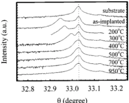
Figure 1 shows the results of共004兲 x-ray diffraction of the substrate, as-implanted and annealed samples. The peak at 33.03° originates from the GaAs substrate. The N implan-tation produces significant lattice-expansion defects as shown by the presence of an additional peak to the left of the
substrate peak. These lattice defects can be annealed out as seen by the movement of the lattice-expansion peak toward the GaAs peak. From the separation of these two peaks, the lattice expansion ⌬a/a was estimated to be 0.22%, 0.17%, and 0.09% for the as-implanted and samples annealed at 200 and 300 °C. After annealing at 500 °C, the lattice-expansion peak disappears and the GaAs peak almost recovers to the original broadness, indicating that annealing can effectively reduce the lattice-expansion defects and recovers the crystal-linity.
As previously observed,3 annealing after implantation has the effect of increasing the sample’s resistance. After annealing at 500 °C, the measured current was less than 10⫺7 A at 100 V on implanted semi-insulating substrates. Because it was difficult to measure such low current at a reasonable voltage, electric characterizations were performed on an-nealed samples using n⫹-GaAs substrates. Figure 2 shows the ohmic current–voltage (I – V) characteristics of a sample after annealing at 500 °C. The current consists of two distinct regions: a linear low-voltage region and an exponential high-voltage region. The inverse of the slope in the linear region was taken as the resistance, shown by the solid lines. Simi-larly, resistance was taken for samples after annealing at 700 and 950 °C and the results are shown in Fig. 3.
As can be seen from Fig. 3, samples annealed at
differ-FIG. 1. Results of共004兲 x-ray diffraction of the substrate: as-implanted and samples after annealing at different temperatures.
APPLIED PHYSICS LETTERS VOLUME 76, NUMBER 16 17 APRIL 2000
2283
0003-6951/2000/76(16)/2283/3/$17.00 © 2000 American Institute of Physics
This article is copyrighted as indicated in the article. Reuse of AIP content is subject to the terms at: http://scitation.aip.org/termsconditions. Downloaded to IP: 140.113.38.11 On: Thu, 01 May 2014 07:53:08
ent temperatures have different temperature dependences. Their activation energies were determined to be 0.34, 0.59, and 0.71 eV for samples annealed at 500, 700, and 950 °C, respectively. After annealing at 500 or 700 °C, the resistance of the samples was found to be about the order of 105 ⍀ at 300 K, which is more than two orders of magnitude higher than that of as-implanted samples. The high resistance ob-served in the as-implanted and annealed samples is believed to be the result of carrier depletion due to capture by traps created by implantation. Because the background electron concentration is about 1⫻1018 cm⫺3 for n⫹-GaAs sub-strates, the trap concentration is expected to be higher than this value to exhibit highly resistive behavior.
The resistance obtained from ohmic contact samples is in general consistent with that estimated from Schottky con-tact samples. The Schottky I – V characteristics at 300 K are shown in Fig. 4 for the as-implanted and annealed samples at 500, 700, and 950 °C. After annealing, forward current is significantly suppressed at large bias, characteristic of resis-tance loading effects. The resisresis-tance was estimated by select-ing the current at a large forward voltage. For example, at V⫽3 V, the current is about 10⫺5A for a sample annealed at 500 °C, giving an R of about 105 ⍀, which is in agreement with that from the ohmic contact sample shown in Fig. 2.
Figure 5 shows the deep-level transient spectroscopy
共DLTS兲 spectra for 500, 700, and 950 °C annealed Schottky
contact samples. The spectra were taken after sweeping the voltage from 0 to⫺2 V. The fill time was set to 5 s at 0 V. The measurement frequency was kept at 5⫻105 Hz. As can be seen in Fig. 5, two groups of traps were detected. One group, denoted E1, was observed around 200 K in 500 and 700 °C annealed samples with an activation energy of 0.32
eV and a capture cross section of 7.51⫻10⫺18 cm2. The other group, denoted E2, was observed around 300 K in 700 and 950 °C annealed samples. Their parameters were deter-mined to be 0.71 eV and ⫽8.88⫻10⫺12 cm2 from the 950 °C annealed sample. Since the peak of the trap was not clearly seen for the 700 °C annealed sample, its parameters were instead obtained from the capacitance–frequency (C – F) spectra shown in the inset of Fig. 5. Two trapping effects can be seen, with the high-frequency capacitance drop corresponding to the E1 trap and the low-frequency drop corresponding to the E2 trap. The parameters of the E2 trap were determined to be 0.69 eV and⫽2.4⫻10⫺12cm2 which are close to those observed in the 950 °C annealed sample. Therefore, the high-temperature traps observed for 700 and 950 °C annealed samples are treated as the same traps.
Based on the results of traps, the increase in the activa-tion energy of the resistance with increasing annealing tem-perature can be explained. For 500 °C annealed sample, only trap E1 was observed and its activation energy共0.32 eV兲 is close to 0.34 eV of the resistance. If a single acceptor trap is assumed in this sample and its concentration is large enough to pin the Fermi level, the measured activation energy of the resistance should be the energy difference between the trap position and the minimum of the conduction band. For the 700 °C annealed sample, E1 共0.32 eV兲 and E2 共0.70 eV兲 traps were observed, both of which should contribute to the resistive effect so that the measured activation energy共0.59 eV兲 of the resistance is the combined effect of these two
FIG. 3. Temperature-dependent resistance of samples after annealing at 500, 700, and 950 °C, respectively.
FIG. 4. Schottky I – V characteristics at 300 K of the as-implanted sample and samples after annealing at 500, 700, and 950 °C, respectively.
FIG. 5. DLTS spectra of samples after annealing at 500, 700, and 950 °C, respectively. The rate window is 0.42 s⫺1. Shown in the inset is the temperature-dependent C – F spectra of the sample after annealing at 700 °C, where two trapping effects can be observed, with the high-frequency one corresponding to the E1 trap and the low-high-frequency one corresponding to the E2 trap.
FIG. 2. Temperature-dependent I – V characteristics of the sample after an-nealing at 500 °C. The resistance was converted from the slope of the cur-rent in the linear region, shown by the solid lines.
2284 Appl. Phys. Lett., Vol. 76, No. 16, 17 April 2000 Chenet al.
This article is copyrighted as indicated in the article. Reuse of AIP content is subject to the terms at: http://scitation.aip.org/termsconditions. Downloaded to IP: 140.113.38.11 On: Thu, 01 May 2014 07:53:08
traps. For the 950 °C annealed sample, only the E2共0.70 eV兲 trap was observed and this trap is believed to pin the Fermi level so that the measured activation energy共0.71 eV兲 of the resistance is almost the same.
Figure 5 shows that the E1 trap decreases in intensity after annealing at 700 °C and disappears after annealing at 950 °C, suggesting that the trap can be annealed out. By comparing to the results of x-ray diffraction shown in Fig. 1, where the lattice-expansion defects are shown to be annealed out also, we suspect that the E1 trap is associated with the lattice-expansion defects by implantation. As for the midgap E2 trap, it was observed in 700 and 950 °C but not in 500 °C annealed samples, suggesting that the trap was created by annealing at a high temperature. However, a simply high-temperature annealing would not produce a highly resistive effect. Since the E2 trap contributes to the observed resis-tances, we believe it is related to the existence of implanted N ions.
The authors would like to thank the National Science Council of the Republic of China for financially supporting this research under Contract No. NSC-87-2112-M-009-022.
1
M. Weyers, M. Sato, and H. Ando, Jpn. J. Appl. Phys., Part 2 31, L853 共1992兲.
2M. Kondow, K. Uomi, K. Hosomi, and T. Mozume, Jpn. J. Appl. Phys.,
Part 2 33, L1056共1994兲.
3
K. Uesugi, N. Morooka, and I. Suemune, Appl. Phys. Lett. 74, 1254 共1999兲.
4S. Sakai, Y. Ueta, and Y. Terauchi, Jpn. J. Appl. Phys., Part 1 32, 4413
共1993兲.
5T. Shima, S. Kimura, T. Iida, A. Obara, Y. Makita, K. Kudo, and K.
Tanaka, Nucl. Instrum. Methods Phys. Res. B 118, 743共1996兲.
6J. Miao, I. M. Tinginyanu, H. L. Hartnagel, G. Irmer, J. Monecke, and B.
L. Weiss, Appl. Phys. Lett. 70, 847共1997兲.
7J. Wurfl, J. Miao, D. Ruck, and H. Hartnagel, J. Appl. Phys. 72, 2700
共1992兲.
8
W. M. Duncan and S. Matteson, J. Appl. Phys. 56, 1059共1984兲.
9K. M. Chen, Y. Q. Jia, Y. Chen, A. P. Li, S. X. Jin, and H. F. Liu, Appl.
Phys. Lett. 78, 4262共1995兲.
2285
Appl. Phys. Lett., Vol. 76, No. 16, 17 April 2000 Chenet al.
This article is copyrighted as indicated in the article. Reuse of AIP content is subject to the terms at: http://scitation.aip.org/termsconditions. Downloaded to IP: 140.113.38.11 On: Thu, 01 May 2014 07:53:08