TU3A-3
Characterization and Modeling of On-Chip Inductor
Substrate Coupling Effect
Chuan-Jane C h a ~ ' . ~ ,
Shyh-Chyi Wong2, Chia-Jen Hsu3, Ming-Jer Chen', and Len-Yi Leu3
Institute of Electronics Engineering, National Chiao-Tung University, Hsinchu 300, Taiwan, R.O.C.*
Acer Laboratories Inc., Taipei 114, Taiwan, R.O.C. Winbond Electronics Corp., Hsinchu 300, Taiwan, R.O.C.Abstract
-
The substrate coupling effects of two adjacent coplanar spiral inductors are characterized and modeled. The noise magnitude between two 45pm-away inductors can be reduced by 6.83 dB by using guard-ring surrounding each inductor, and improved by 10.28 dB further by adding patterned ground polysilicon shield beneath at 3 GHz. The inductor with patterned polysilicon shield beneath shows improved quality factor and noise isolation. Moreover, a macro model is presented for modeling quality factor and inductance of on-chip spiral inductor and associated neighboring inductor's coupling noise effect.I. INTRODUCTION
The inductor is one of the key elements in monolithic RFIC designs such as amplifiers, mixers, filters and oscillators [ 1][2]. For silicon technology, the significant coupling noise through lossy substrate is a big issue. The characterization and modeling [3][4][5] of s-parameters, inductance, quality factor, and coupling effect of coplanar spiral inductors are essential to optimize the RFIC performance and to minimize chip size and coupling noise by proper design and placement of components.
Reported here is the coupling effect of on-chip coplanar spiral inductors for various schemes, which has never been studied in previous works to the authors' knowledge. A correspondent model to characterize the coupling effect, integrated with single inductor's intrinsic high frequency characteristics, is presented. The inductor model can be used for the simulation and optimization of inductors' coupling noise, placement, and chip area.
11. COUPLING EFFECT OF ON-CHIP COUPLED COPLNAR SPIRAL INDUCTORS
A . Experimental Setup
A 0.25pm 5-level metal CMOS technology is used to fabricate the on-chip spiral inductors. The P-type substrate resistivity is lOQ-cm, M4 and M5 thickness are 5700A and 1 OOOOA, respectively, and the oxide dielectric thickness between M4 and the substrate is about 56000A.
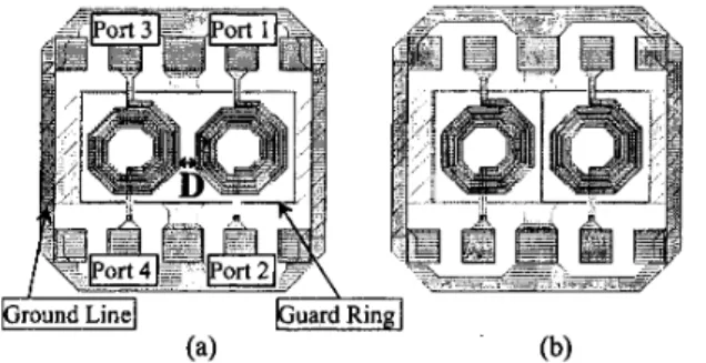
A 3.5-Turns octagonal spiral inductor is designed by using M4 and M5 stacked to form the coil and M3 to form the underpass. The layout representations of main configurations of coupled coplanar inductors are shown in Fig. 1. Fig. l(a) shows the inductors without guard-ring within, and Fig. l(b) shows the inductors with guard-rings within, and with or without patterned ground polysilicon shield beneath (PGS-inductor). A variety of inductor distances (D) are designed. M5 terminals are defined as port 1 and port 3; while, M3 terminals are defined as port 2 and port 4. The inductance (L) and quality factor (Q) in this paper are measured and extracted from the inductor between port 1 and port 2. For coupling noise measurement, a RF signal is forced to port 3 and the port 2 is sensed to measure the coupling noise (S23). All ground lines and guard-rings for coupled coplanar inductors are shorted together, and the spacing from guard-ring to coil is 20 pm.
UI
RtE
(a) (b)
Fig. I. Different configurations of on-chip coupled coplanar inductors with port numbering.
S-parameters are measured using Cascade Microtech G-
S-G RF probes and an HP8510C Network Analyzer. Pad parasitic is de-embedded by subtracting out open-pattern's y-parameters. The two-port measurements are done as the other two reminding ports are floating. L and Q are extracted from the de-embedded Z-parameters using
imag(Z1port)
.
imag(Z:lport)&f
9 = real(Zip0rt)And the coupling-noise is defined as the magnitude of L =
de-embedded SZ3. 157
B. On-Chip Coupled Inductors
B. 1. - Inductance, Quality Factor, and Self-Resonant
Frequency of Single Inductors
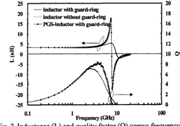
First of all, for various single inductor configurations, the L and Q characteristics are investigated and shown in Fig. 2. At low frequency, all configurations show similar L and Q performance. There is no difference for L and Q of inductors with and without guard-ring. The previous work [6] indicated the Q of PGS-inductor could be improved 33% at 2GHz. In our experiment, the maximum Q is raised from 7.21 (at 2.7GHz for inductor without pattemed ground polysilicon shield) to 8.39 (at 3.7GHz for PGS-inductor). And the maximum improvement of Q is 72% at 5.6GHz with the addition of patterned ground polysilicon shield. For PGS-inductor, the thinner dielectric thickness from coil to pattemed polysilicon shield layer results in larger parasitic capacitance and lower self- resonant frequency (FSR). As the frequency is near FSR, the inductance's drastic transition of PGS-inductor implies that the lower parasitic resistance, due to low resistance's patterned polysilicon, is in parallel with substrate parasitics. The lower parasitic resistance contributes to the observed Q's improvement of PGS-inductor.
10 - 5 5 0 cl -5 -10 -15 -20 -25 20 18 16 14 12 10 0 8 6 4 2 0 0.1 1 10 100 Fresueney(-)
Fig. 2. Inductance (L) and quality factor (Q) versus frequency. B.2. Coupling Noise Effects of Coupled Inductors
Coupling noise through substrate is a critical issue for lossy substrate technology like silicon substrate. The realization and isolation techniques of coupling noise are crucial for the compact and confident RFIC layout and design. RF noise isolation can be improved by using grounded substrate guard ring surrounding the inductor [8] and/or patterned ground polysilicon shield beneath [6]. We investigate coupling noise effects of two closely placed coplanar spiral inductors for various configurations here.
The comparison of coupling noise on various distances (D) between two coupled inductors, with and without guard-ring within, is shown in Fig. 3. The equivalent
circuit of coupled inductors, between port 3 and port 2 in Fig. 1, at low frequency can be approximated to be the one as shown in Fig. 4 and its S-parameter s b , is derived (Eq. 1) under the conditions of low to be
frequency and
kubc
being much larger thankub,
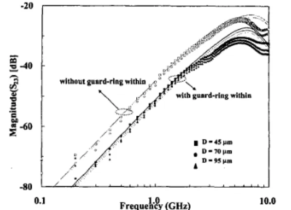
where s = jw. At low frequency, Fig. 3 shows the initial slope of the S,, of 40 dB per decade, this is due to a couple of dc zeros [9]. The existence of two dc zeros implies that the S,, is proportional to s2 with substitution of s = jw. The measured coupling noise characteristic agrees well with the derived equation, Eq. 1. The two dc zeros are created by the CO,, of two coplanar inductors, in series. The larger coupling noise for higher frequency, owing to the two zeros, results in that the coupling'noise needs to be considered more carefully for higher frequency application. At medium frequency, the magnitude of SZ3 turns down by -20dB per decade of frequency as frequency increases above 6GHz. The -20dB per decade indicates three poles occurring around this knee-point frequency. Two poles depend on the coil-to-substrate capacitors (C,,) and the two kinds of substrate resistances ( k u b andkubc);
and the third pole depends on the core inductive characteristics of inductors. The frequency ofknee-point can be derived by ( ~ ~ s u ~ C O X ) - ' . At frequency above 15GHz, the substrate capacitance between two inductors will lead the increase of S23 again, as observed
2 ( S cox) &ub2 Rsubc in Fig. 3. -20.0 -30.0 c
3
-40.03
,k -50.02
8
-60.0 -70.0 -80.0 0.1 Coupled inductors without guard-ring Coupled inductors with guard-ring withinFrequency (CHz) lo 100
Fig. 3. Coupling noise versus frequency for various coupled coplanar inductor configurations and distances D.
node a
t F ~ k - e
node bFig. 4. A equivalent circuit of coupled inductors. The coil-to- substrate capacitors of two coupled inductors are modeled by Cox. The resistance between the top substrate surface under inductor and the guard ring and the resistance between the two inductors are represented by
Kub
andKub0
respectively.As shown in Fig. 3, the 6.83dB improvement of S,, at 3GHz is obtained for couded inductors of D 4 5 ~ m with
111. MACRO MODEL OF COUPLED SPIRAL INDUCTORS FOR COUPLING EFFECT
m
-
.- .
! -35
I:
guard-ring within than tha; without guard-ring within. The within guard-ring can improve the noise isolation well at low frequency, even at high frequency. The significant improvement is because that the fraction of substrate noise is shunted to ground effectively through the path of within guard-ring pick-up, not coupled to neighboring inductor. While PGS-inductor configuration with guard-ring (GR) within can give much better noise isolation characteristic for frequency below 9.6GHz than conventional inductor with GR within. It also has S,, at 3GHz 10.28dB lower than inductor without PGS but with GR within, and 17.1 1 dB lower than that without either PGS or GR within. The coupling noise can be effectively reduced by using the within guard-ring, and further enhanced by using the beneath-inductor patterned ground polysilicon shield.
Because the typical silicon substrates are resistive up to several GHz [3], the Sz3 is inversely proportional to
kubc
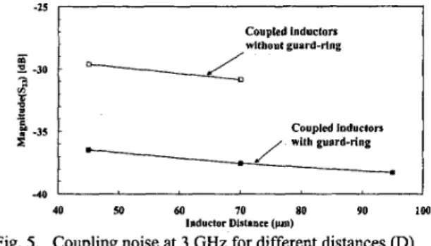
as shown in Eq. 1 . Fig. 5 shows the coupling noise effects versus coupled inductors distances at 3GHz and the distance coefficient with guard-ring within is simplified to 0.037dB/pm for a limited distance range. The linear- spacing-dependence is easy to use for the optimization of layout. The frequency limit of resistive substrate could be estimated from the relaxation time constant (T = ~ ; p =1.05- IO-IIsec) of typical substrates and the frequency at which the skin depth becomes comparable to the substrate dimensions (The characteristic fiequency for skin-effect in Si-layer is p/npo.tsi
,
where tsi is the thickness of silicon layer [IO]). Thus, based on this evidence and theory, we developed a lumped-circuit model by adding substrate resistors only between two inductors to emulate the substrate coupling effect in Section 111.The low distance coefficient in Fig. 5 implies that the significant coupling noise reduction will result in large chip area penalty. Thus, the effective substrate noise isolation techniques with maintaining compact chip size are important for RFIC design.
- Coupled inductors J with guard-ring I i -15
I
t
Coupled inductorsI
without ward-rlnl! -40 L JFig. 5. Coupling noise at 3 GHz for different distances (D).
40 so 60 70 80 90 100
Inductor Distance (pm)
Several equivalent-circuit models have been developed and successfully used to model most on-chip spiral inductors [I 1][12][13][7] for designing RF IC's. In order to accurately characterizing the eddy current effect and the skin effect, the model presented in [7] is adopted for modeling each single spiral inductor. In Fig. 6(a), the spiral coil structure is represented by an ideal inductance L,, a series resistance $, a series composition of
k,
and Lsk in parallel, external connection wires inductance L,, andL,,,
and an inter-wire capacitance C,. The shunt parasitics result from a combination of oxide capacitance (Coxlr Cox,) between coil and substrate and substrate parasitics ($ubi, Csubl, CsubZ). As a result, the model for inductor with guard-ring shows good agreements with measured L and Q in Fig. 7. And the errors of both real and imaginary parts of S-parameters are below 10% for frequency lower than 5.7GHz. Similarly, the model of PGS-inductor also is implemented with same accuracy.(a) nod# 1 node 2 4 4 node 3 node 4 Ahl (b)
(4
Fig. 6 . (a) Lumped model for single inductor. The resistive networks for the coupled coplanar inductors configurations: without GR within (c) and with GR within (d).
12 10 8
I 6
A 4 2 0 2 8 6 4 2 0 0 2 4 0.1 I .O 100 Icon Yrequmcy(G€k)Fig. 7. L and Q for inductor with guard-ring. All parameters for the lumped models are shown in Parameter List Tables.
For modeling the substrate coupling effect of coupled inductors, two simple resistive networks are presented in Fig. 6 (c) and 6(d). This macro models are for the first order estimation of coupling noise and are easy to extract. The single inductor model in Fig. 6(a) is represented as a four-port sub-circuit in Fig. 6@). For coupled inductor configuration without GR within, the resistive network for
coupling effect is composed by four
kUbc
as shown in Fig. 6(c). The parasitic substrate resistance between two coupled inductors is characterized by 7c model. Four $rare added as Fig. 6(d) for modeling the effect of guard- ring addition for coupled inductors with GR within. The four
Rube
and $r values can be assumed to be same,respectively, for the symmetry layout. Then,
kubc
and$I
can be extracted out individually by modeling S23 characteristics of coupled inductors without and with GRwithin in sequence. Fig. 8 shows, at frequency below several GHz, the good agreements of simulated and measured S23 for various coupled inductor configurations with D=45pm. However, as frequency up to 0.6GHz, the phases of the S,, start to drop from 180: that is 7c (radian). The descending slopes also indicate the poles exist as explained previously in Section 11. The frequency of knee- point of Mag@,,) can be estimated by (2ldzs~bCox)-'
-
6GH2, where h u b and Csub are from the inserted table in Fig. 7, which shows good agreement with measurement results. In this macro model, the parasitic effect for coupling noise simulation at frequency near or above self- resonant frequency is not considered in order to simplify the model but to preserve the accuracy within the application frequency range. The
kubc
should be distance- dependent resistance and extracted from coupling noise characteristics of coupled inductors with various distances D. The distance coefficient is 6 Wpm; that means, thekubc
is 13500 for D=70pm and 15000 for D=95pm. The simulation results with the distance coefficient are shown in Fig. 9, as compared with measurement data. Thus, enough accuracy can be obtained by simple resistive network we present and the macro model is helpful to optimize the coupling effect and simulate whole chip's complete characteristics. - - - 20 I 1 4 - 2 - 0 8E
-2 3s
v Hi
- 4 -6 c -8 0 iii Ps
83
4 0 h R -20 M -605
-80 J ' ' " " " ' ' ' " " " ' ' '""'
-10 0.1 1.0 10.0 100.0 Frequency (GHz)Fig. 8. Comparison of macro models for SZ3, where
Kubc
are 1.2 KR andRpr
are 190 0.IV. CONCLUSION
The characterization on coupling effect of on-chip coplanar inductors has been presented. The inductors with guard-ring within have significant noise isolation improvement, even for high frequency above 10 GHz. The PGS-inductor can enhance quality factor and noise isolation performance simultaneously. We develop the circuit simulation macro models with simple resistive networks to consider the coupling noise effect for coupled inductors as well as the inductor's intrinsic characteristics.
-20
,
II
, : / ,:;//
/,
D - 1 0 p m A D-95)m*I
, .
/.
, , , , , , , I 10.0 Freque?i& (GHz) 0.1Fig. 9. Coupling noise of macro models vs. distance dependence. REFERENCES
L. E. Lamn, "Intepted circuit technology optiom for RFICs
-
J. N. Burgha& et al, "RF circuit design aspects of spiral inductors onR Gharpmy et al, 'Modeling and analysis of substrate coupling in integrated circuits," IEEE CICC, pp. 125,1995.
M. Werthen et al, "Investigation on MMIC inductor coupling e f f i " IEEE iWIT-S Digest, 1997.
A. sa" et al, "Desigwriented subsbate noise coupling
" o d e l s for heady doped CMOS ",p" IXAS, pp. 218, 1999.
P. Yue et al, "Onchip s p d inductors with patterned ground shields for Si-Based RF ICs," IEEE JSSG33, pp. 743,1998.
C. J. Chao et al, "charactenza ' tion and modeling of on-chip spiral
inductors for Si RF ICs," accepted for IEEE TSM.
A. Pun et al, "Expenmental results and simulation of subsbate noise present status and future directi~n~," IEEE JSSC-33, p ~ . 387,1998. ~ i l i ~ n , " IEEE JSSC-33, pp. 2028,1998.
coupling via plan& spiral inductor in RF ICs," IEDM, pp. 325,1997. technology," JEEE "EM, pp. 2252,1997.
[9] J. P. Raskin et al, "Substrate crosstalk reduction using SO1
[10]H. Hasegawa, 'Roperhes of microstrip line on Si-Si02 system,"
[11]Ali M. Nhejad et al, ''Numerically stable Green W o n for modeling and analysis of substrate coupling in inkgated circuits," IEEE Trans. 0 - 1 7 , pp. 305,1998.
[12]R Groves et al, "Temperature dependence of Q in spiral inductors
fabricated in a Silicon-Gemanium43iCMOS technology,"
IEEE
BCIl4,pp. 153,1996.
[13]John R Long et al, 'The modeling, characterizab 'on, and design of monolithic inductors for silicon RF ICs," JSSC-32, pp. 357,1997. EEETran~.iWIT-l9,pp. 869,1971.