Proceedings of the 3rd European Microwave Integrated Circuits Conference
5.5 GHz Low Voltage and High Linearity
RF CMOS
Mixer Design
Senhg-Feng
Lul
andJyh-ChyurnGuo2Institute
ofElectronics, National Chiao-Tung
University, 1001Ta-Hsueh
Rd,
Hsinchu,
Taiwan, R.O.C. 1sflu@seed. net. tw2j cguo@mail. nctu. edu. tw
Abstract-A CMOS mixer was design with a new circuit scheme II. CIRCUIT DESIGN PRINCIPLE
torealize low voltage and high linearity simultaneously. A double A
5.5
GHzdown-conversion mixer aimed forhigh linearitybalanced Gilbert cell was adopted as the basic topology and
...
vat yer low voltage to 1-V was desi ned with a new circuit
TSMC 0.18pm 1P6M CMOS process was employed for the on- . g g
chip RF circuit fabrication. The proposed new circuit scheme scheme. The full circuit s composed of eight
circuit
blocks as consists of LC-tanks as a capacitively coupled resonator for low shown in Fig.2. They are arranged with three on-chip and five voltage and multi-stage parallel RC networks for linearity off-chip elements, respectively. The three on-chip elements improvement. Furthermore, multi-gated structure is applied at incorporate a pair of multiple-gate RF amplifiers [2], local the RF input as a transconductance amplifier to enhance switches (LO), and load IF circuits, denoted by the solid-line conversion gain and linearity. The new circuit scheme enables a box. The off-chip circuits represented by dash-line box coversuccessful low voltage operation at 1-V for 0.18,um technology, five elements, such as parallel LC-tanks, bypass capacitors, The measured circuit performance demonstrates superior RF baluns, LO baluns, and a measuring circuit. QFN package linearity with 11P3 of 11 dBm and P1dB of 2.2 dBm. The is
adopted
tointegrate
theon-chip
andoff-chip
circuitsconversion gain can be maintained at 8.1 dB in a wide together. Fig. 3 displays the full circuit schematics in which frequenciesof 5GHz to 6.8GHz. the circuit topology correspondingtoeach functional block in
I. INTRODUCTION Fig.2isclearlydefined.
Mixer is one of the most
important
elements in RF front- To realize a lowvoltage
design,
capacitively coupled
LCend
constituting
the modern communicationsystem.
The well tanks firstproposed by
Mankuet al.[1]
areemployed
inthis known Gilbert cell as shown inFig.
1 is the mostgenerally
down-conversion mixerdesign.
As shown inFig.3,
apair
of used mixer architecture due to its advantages in port-to-port LC tanks aredeployed
at drain terminal of RF isolation andspurious
output
rejection.
However,
the transconductancestage
for1-V
supply voltage.
Onemorepairtraditional Gilbert cell mixers generally suffer a limitation in of LC tanks are allocated at the source
terminal
of LOvtragsc.ialindert tel cascadesraucure
wit
tacked
switches and ended to theground. Ideally
for inductors freevltranesit
ingsere
withe
ccadresstoru.
ct
realize
lowvtage
from series resistances, the LC tanks can enable a shortpathoperaitsion
cpiivel
couplresso.
Ti
element,
e.g.tL
atDCandanopenpath
atresonance. Inpractice,
the existencetankstwere *propsed
anddemd
onatith
themappl,
ic.a.t
i ofseries resistances ingeneral
inductors leads to a very lowink
R crcuise[1].
Heve, poor
larity
fhe
ature
bylow
impedance
atDC state whereasaveryhigh impedance
underinP
(appearss
]aswevea,cooritic eakntyfessandremdsb
o a RFoperation.
In this way, the DCvoltage drop
across theIIP3
(-6dBm)
appears as a critical weakness and demandls a stce trcuewt nd Osae nFg3cnbsignificant
improvement.
In this paper, a new circuit schemestaced tructure
tandl
LOstages
in Fig.3 canbe
adopting multi-stage parallel
RC networks isproposed
andrdi
toerl
asnerstage to
rminimize
the power imlmne to aciv suero linartydissipation.
As forRF
operation at resonance, the LC-tanks vcc becomesanearlyopenpathand thebypass capacitorcanpassEr theRF signalacross RFand LO stages.
Vcc DC)
AL__jOff-ChipCircuit Loa Elremt
circuit
MOn
ChipCircuit IF Output 1IF + r---_- - IleasureCircuitL.I
LO Balun LO ElementCircuit
O-
VI
3M r
M4M5
M9
I-
O7I
Tank
1
|
LC-Tank|
LO - IVcc(DC) Vcc (DC)
R F + 0-1 mL1 M v R F - + Bypass +
LC-Tankl CapacitanceL LC-Tankl
L 2Circuit 2JCircuit I
>~~~~~~~~~~~~R
Bau Mut-gtORF
___'1 E R F B a u n- r- Elemrnent CirScuIt|
Fig. 1 CMOS Gilbert Cell mixer architecture Fig. 2 CMOS RF mixer circuit block diagram
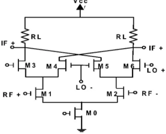
Vcc bonding pads. Fig. 5 presents the bond-wire package model. The series inductance is approximately lnH/mm. For a bond wire with a length generally exceeding that of the on-chip
T
>- 1< > inductor, it will impose a significant influence on the circuit-IF
. + IF'performance.
Duetothefact,
thepackage
model of bond-wireQ5
1
|
Q6Q7 1Q8 mustbe taken intoaccountinthe full circuit simulation.Fig.
6r
_____r_
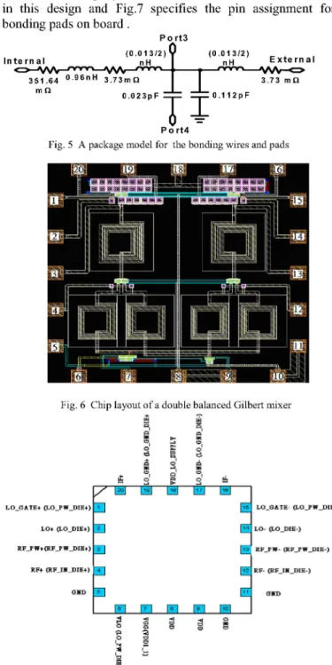
L illustrates thechip layoutof the double balanced CMOS mixerin this
design
andFig.7 specifies
thepin assignment
forbonding pads
onboard.Vcc Port3 7 (0.013/2) (0.013/2) Internal nH nH External 351.64 0.96nH 3.73mn l 3.73 mQ mn t0.023pF 0.112pF
~~~~~~~TIE
Q1 2 Q3 Q40 Port4-Fig.5 Apackagemodel for thebondingwires andpads
RFK + RF
-¢ ¢ ~~VDD1 VDD2
Fig.3The circuit schematics ofadouble balancedRFCMOSmixer with
RFstage, LOswitches,LObias, IFload, LC-tanks, bypass capacitor, and
LEM_
balunsRegarding a major target for high linearity, multi-gate transistors [2] were designed in the RF transconductance amplifiers for verification. The third-order nonlinear term cancellation realized by gate bias tuning on the multi-gated structure can help improve linearity. Besides, a new design withmulti-stage parallelRCnetworks wasimplemented atthe IF output tofurther enhance linearity. Simulationas shown in
Fig.4 indicates that the multi-stage parallel RC networks Fig. 6 Chip layout of a double balanced Gilbert mixer adoptedatIF stage, actingas ahigh-passfilter caneffectively
suppressthe higherorderharmonic components andpush out the third order intercept point. Through this mechanism, the linearitydefined byIIP3 canbe significantly improved. As to
design for higher conversion gain (CG), inductive i
degenerationwas implemented by an on-chip inductor at RF
output[3].Note thatan inductor of 3.799nHwasused in this LOGATE4
(LO4_PW_DEK)
LO_GATE-OPW-DIdesigntooptimizethe outputmatchingandimproveCG. LO+
(LIO
DIE+ LO-(LODIE-)
.0 . l |
0.0 RFJPWt(RJW_DIEt) RFPPw-(I"WW
DE---2.0
RFt(RFJN-DIE+) 4 1RF-(RFI_EDH-)
--4.0
c1i-m -0.51i l--6.0 m 1 1 @BD
IF loadw]IF load: 8.0
IFloadwocapacitor RCnetworkswicapacitors
..,,,,,,l/,,,,,,,,,,,,,11...
..
-1.C
110.00
0 1 2 3 4 5 6 7 8 9 10 0 1 2 3 4 5 6 7 8 9 10
Freq(GHz)FriFreq(GHz)
Fig4(a)IFstagewithsimple resistor network without capacitor (b)IFstage Fig. 7 Pin assignment for mixer chip on board bondingpads
withparallelRCnetworks-theparallerlRC serves as ahigh-pass filterto
effectively filterouthigher order harmonics and improve lineariy
III. RESULTS AND DISCUSSION
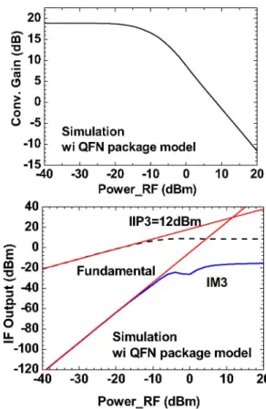
Eventually, the full circuit has to be mounted on PCB for A Smlto eut measurement. The critical points to be considered are the A.SmltoReus
parasitic inductance and resistance existing with the bond 0.18um MOSFET model was employed for on-Si-chip wires and the parasitic capacitance originated from the circuit simulation and SPIL QFN package model was
integrated with core MOSFET model for a full circuit 20 simulation. Fig.8(a) and (b) present the CG,
PIdB,
and IIP3under varying RF power, simulated using SS corner model, 15 under 1-V and 250C operation. Table 1 summarizes the full
circuit simulation results
using typical
andcornermodels(TT,
SS, FF) for MOSFETs as well as QFN package model for o 10 bonding wires and pads. The operation condition for the low
voltage mixer is a supply voltage at 1-V and temperature at
25°C. The key performance parameters include conversion 0 5 gain (CG), gain compression
(PIdB),
the third-order interceptpoint (IIP3), and power consumption.
The simulation predicted a good performance of high CG, -50 -40 -30 -20 -10 0 10 high linearity, and low power consumption. The power Power_RF (dBm)
consumption at 1-V can be push to 2-3.7mW. The high 15
linearity is featured by IIP3 of8.2A12 dBm and 1dB output E 10 OP -622dBm power compression
(OPIdB)
of 4.89-6.22 dBm. CG can 5 ldBachieve 18.7>24.2. The high linearity is realized through the o
multi-stage RC networks at IF load.
-0
TABLE I 1
Simulation results foramixeronQFNchip operating underl.OV and25°C m
(TT Typical,SS Slow,FF Fast) 20
Performance Parameters SS TT FF 0 -25
Conversion Gain(dB) 18.7 24.2 19.8 I -30
OPIdB (dBm) 6.22 5.8 4.89 -35 _
IIP3 (dBm) 12 10 8.2 -50 -40 -30 -20 -10 0 10
Power Consumption (mW) 2.03 2.74 3.71 Power_RF (dBm)
RIF/LO:5.5/5.499GHz, LO power: 2.5 dBm
Fig.8(a) Simulated conversion gain andIIP3underl.OVand250,SScorner
B. Measurement Results modelwasused for simulation
The measured
PIdB
and IIP3 are demonstrated in Fig. 9(a)and (b). The superior linearity with IIP3 of 11 dBm and
PIdB
20of 2.2 dBm proves the success of harmonic suppression m 15 X
throughthehigh-passfilterrealizedby multi-stage parallelRC 1 networks atIF load. IIP3 ashigh as 11 dBm at LO power of
2.5dBm matches very well with the simulation result of 12 5 dBm shown in Table 1. Fig. 10 (a) and (b) present the _ 0
measured CG vs.
input
powerandRFfrequency
in which CG 0 Suiabove 8.1 dB can be maintained over a wide range ofinput
S10
wiQ pacg power to OdBm and frequencies in 5-6.8GHz. ThewiQFNpackagemodel
degradation compared with simulation suggests a deviation -15 -30 -20 -10 0 10 20 from the desired optimal matching incorporating the circuit Power RF(dBm)
elements on PCB, such asLC tanks and balun. Improvement
-can be achieved by an extensive calibration on the package 40
model and that for on-board circuit elements. Table 2 20 _
summarizes the measured performance parameters, such as 0 - -CG,
PIdB,
IIP3, and power consumption. The measured power m -20consumption appears higher than simulation prediction. Fundamental
Process variation induced drift in resistances and IR drop is -M0
considered a potential reason responsible for the increased Q-60/ DC power. Fortunately, the power consumption keeps low at °-0 L
around 4 mWattributed tothe sufficientlylow voltage to 1s.OV. L Simulation
TABLE 2 -100 / Wi QFN package model
MeasurementResults undersupply voltage at1l.OV,Temp=25°C -120 I , , ,
Performance Parameters rMeasured Results l -40 -30 -20 -10 0 10 20
Conversion Gain 8.1 dB(0dBm
p1dB 2.2 dBm Power_RF (dBm)
IIP3 11 dBm Fig. 8 (b) Simulated conversion gain and IIP3 under 1.OV and 25°C. SS
Power Consumption 4.lmW corner model for MOSFET andQFNpackage modelforbonding wires and RF/LO: 5.501/5.5GHz, LO power:2.5 dBm pads were adoptedforthe full circuit simulation.
20 IV.CONCLUSION
10 r - PIdB2r7nrTvr...2dBm
...A
;v 25.5 GHz down-conversion mixer has been fabricated inco f0.18 um RF CMOS technology. The new circuit scheme
_0 , enables a successful low voltage operation at
1.OV
and lowpower
consumption
of around 4mW. This lowvoltage
mixerX ,/ demonstrates
superior linearity
with11P3
of11 dBm andP1dB
-20 of 2.2 dBm. The conversiongain canbe maintained at 8.1 dB
over abroadband operationin5GHz to 6.8 GHz.
0 -30- ,
X -30 The
superior linearity
in terms ofhigh
11P3
andPIdB
proves-40 theadvantagerealizedby mutli-stage parallelRC networks at
-6 .. .. .. IF output. The success of low voltage operation validates a
new
design adopting
LC-tanks at RF and LOstages.
TheRF_Power_In (dBm) major challenge remained with this work is a certain deviation 20 F between the wholeIIP3=1
<
1dBmchip
simulation and measurementresult. It is because that simulation accuracy isacceptable
for onchip
m 0 Fundamental balun and LC tank
design; however,
afully
qualified
-10 simulation tool islackingfor balun and LC tankdesign, which
-20 is on PCB through themethod of SMD. The PCB layout can
0-30 be improved by considering the characteristic wavelength of
a.
-40 microstrip lines. Regarding balun circuit design, a
0.-5O t
jreplacement
/ of conventionaldesign using passive
components-60
° -70 --Fundamental by active components [4,5] can
further
improve the circuit-80 -- IM3 performance and reducethe
chip
area.-90
-40 -30 -20 -10 0 10 20
RF_Power_in (dBm)(Tonel,2) ACKNOWLEDGMENT
This work was supported in part by NSC under Grants
Fig.9 Measured linearity(a)P-ldB and(b)IP NSC95-2221-E009-289 and NSC96-2221-E009-186. Also,
12 the authors acknowledge the support from NDL CiC for test
10 *
chip
fabrication and RFLab. formeasurement.
REFERENCES ._ 8
v6 \
[1]
T. Manku, G. Beck, and E.J. Shin, "A low-voltage design0 o .
~~~~~~~~~~~~~~~~technique
for RFintegrated circuits,"IEEETrans. Circuitsand>4 \ q SystemsII,vol.45,pp. 1408-1413, Oct. 1998.
> \ [2] B. Kim, J. Ko, and K. Lee, "A New Linearization Technique
0> 2 F \ X for MOSFET RFAmplifier Using MultipleGated Transistors,"
IEEE Microwave and Guide Wave Letters, Vol. 10, No.9,
0
pp.371-373,
2000.-40 -35 -30 -25 -20 -15 -10 -5 0 5 10 15 [3] B. Razzavi, RF Microelectronics, New Jersey, Prentice-Hall,
RF Power in(dBm) 1998.
[4] I. J.Lin, C. Zelley. 0. Boric-Lubecke, P. Goddl and R. Yan, "A
10|-|-|--~|e
~silicon
MMIC Active "A silicon MMIC active balun/bufferX 8-
amplifier
withhigh linearity
and low residualphase
noise,"inv~
6\-.
2000 IEEE MTT-SInternational
Microwave Symposium Din.,._ \ vol. 3.pp.1289-1292
(D4
[5] H. Koizumi, S. Nagata, K. Tateokq K. Kanazawal and D. Ueda,.° 2 "A GaAs Single balanced mixer MMIC with built-in active
en . ~~~~~~~~~~~~balunfor personal communication systems," in IEEE @ ° t \ 1 Mi~~~~~~~~crowaveand Millimeter- Wave Monolithic Circuifs
o -2 \ Symposium, May. la5- K.61e995pp.77-80.
C
~
RF inputpower:* OdBm \ -65.0 5.5 6.0 6.5 7.0
RF_in_Frequency(GHz) Fig. 1b0(a) Measured conversion gain vs. RF input power
(b) Measuredconversion gain vs.RF