A
Single Chip CMOS
APS
Camera with Direct Frame Difference Output
Shyh-Yih Ma and Liang-Gee Chen
Department of Electrical Engineering, National Taiwan University
I . Roosevelt Road Sec. 4, Taipei 106, Taiwan
-
0 0-
-
:
a Abstract--
APS array (128x96) Chip ArchitectureA CMOS active pixel sensor with direct frame difference output is reported i n this papcr. The proposed pixel circuit includes a photodiodc and 9 transistors and is optimized for low voltage operation. A 128x96 pixel prototype camera chip with an on-chip %bit pipeline ADC was fabricated in a 0.Spm double poly double metal CMOS process. At 3.3V, the power dissipation is 56mW.
Introduction
Active pixel sensor (APS) ( I ) is a very promising approach for camera-on-a-chip systems because it uses standard CMOS process and therefore can be integrated with control and signal processing circuits to form a complete camera system. The complexity and cost of the whole system can be grcatly reduced if the APS and carefully chosen signal processing functions are integrated in the same chip.
For video applications, the motion information is essential for video comprcssion, motion detection, and moving object segmentation. The complexity and computation load of the following signal processing units in these systems can be dramatically reduced if the camera can provide the frame difference output in addition to the current frame image. The traditional photo diode APS can not deliver the frame difference output. The photo gate APS has been shown (2) (3) to be capable of acquiring frame difference output. However, when the sensor is operating in this mode, the exposure time of the pixel is fixed and is equal to the frame period. A new cell circuit should be developed if both the frame difference output and electronic shutter function are desired.
Low voltage operation is another concern. In order to integrate the APS with advanced signal processing circuits that use lower supply voltage, the APS should be operated in low voltagc, too. As a result, the signal swing is reduced. Care should be taken when designing the sensor cell circuit to maximize the signal swing in low supply voltage. We proposed a low operating voltage APS cell circuit with direct frame difference output. The architecture of the camera chip is described in the next section. Then, the design and operation of the cell circuit is discussed. Finally, the experimental results are analyzed and the conclusion is given.
13.2.1
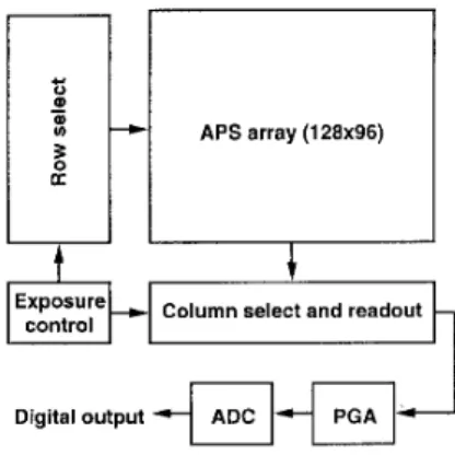
Fig. 1 shows the block diagram of the CMOS APS camera with direct frame difference output. The image-sensing portion is a 128x96 active pixel array. To the side of the sensor array is the row select circuit that controls the reset, exposure, and readout timing of the sensor cells. The pixel data in the selected row are then read out sequentially by the column select and readout circuit. After that, a programmable gain amplifier (PGA) is used to control the magnitude of the image data. An 8-bit pipeline ADC with digital error correction (4) (5) is used after the PGA to perform the analog-to-digital conversion. The signal paths are fully differential in the sensor cells, readout circuit, PGA, and ADC. Therefore, direct frame difference readout can be achieved.
Column select and readout
Digital output
+qiFl
I
Fig. I . APS camera chip block diagram Sensor Design and Operation
A . Cell Design
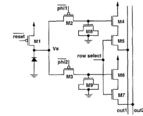
The APS cell circuit with direct frame difference output is shown in Fig. 2. The photo site is a photo diode formed by N-diffusion and P-substrate. In contrast to the traditional APS cell circuit, our cell circuit has two sample and hold sections and two signal readout paths for direct frame difference output.
A sample and hold section consists of a sampling switch and a holding node. The sampling switches (M2, M3) act as electronic shutters to control the exposure time of the pixel. The holding nodes are at the gates of the source follower
287
transistors
(M4, M6).
However, the reverse biased P-N junction leakage current at the drain node of the shutter switch can destroy the signal if the capacitance at the gate of the source follower is too small. Two MOS capacitors (M8,M9) are added at these nodes.
The reset switch (Ml) and two shutter switches (M2, M3)
are PMOS devices in our design while other transistors in the cell circuit are NMOS devices. Usually, all transistors in the cell circuit should be of the same polarity to avoid the large well spacing in the pixel layout. However, when the power supply voltage is low, the signal swing becomes the main concern.
If
the reset switch is an NMOS device, the reset voltage of the photo diode is one threshold voltage lower than the power supply voltage (Vs=V,,-VT,). The threshold voltage (V,,) of NMOS devices with body effect is about 0.W to lV, which is a significant part of the signal swing in low voltage operation. Therefore, we use PMOS devices as the reset switch (Ml) and the shutter switches (M2, M3) to eliminate this voltage drop. In this way, the signal swing is maximized at the price of a slightly increased cell area, which is acceptable in our application.U "S
I
4
1
I 1
I
OUt2.Fig. 2. APS cell circuit with frame difference output
B. Operation
Two operation modes are available in our APS camera chip, one is intra frame mode that reads out the current frame image, the other is frame difference mode, which reads out the difference between two consecutive frames.
In frame difference mode, the two electronic shutters turn on alternatively as shown in Fig. 3. In each frame period, only one of the electronic shutters turns on. The other shutter switch remains open during the whole frame period so the current frame sensing operation does not affect the previous frame signal stored in the pixel.
The timing diagram of the APS cell operated in intra frame mode is shown in Fig. 4. As can be seen from the figure, one of the shutter signals is activated in each frame period while the other shutter only turns on in the reset phase and
then turns off in the exposure phase. Therefore, one of the sample and hold sections stores the current frame pixel data and the other sample and hold section stores the reset data. The output is taken differentially from the two output lines
so the intra frame image data can be obtained.
,,,,Iu
U U U-
phli phi2L
-
row select1
n
n
n
OUti QUtPFig. 3. Timing of APS cell circuit operated in frame difference mode.
-
reset U U U
row select
1
n
n
OYti
out2
Fig. 4. Timing of APS cell circuit operated in intra frame mode.
C. FPN Suppression
Fixed pattern noise (FPN) caused by device mismatch and process variation has been a major problem with APS because it has multiple readout paths. The traditional solution is the correlated double sampling (CDS) technique. The mismatch in device. characteristics is cancelled by reading out the pixel data twice, one for the signal value and one for the reset value. Since the two values pass through the same signal path, the influences of the device characteristics are cancelled by taking the difference. W e use the CDS concept to reduce the FPN. Fig, 5 shows the structure of the cell array. At the bottom of the APS cell array, an additional row of APS cell is added (6). A metal layer covers the whole area of the pixel circuit in this row to prevent any incident light from reaching the photo diode. In this way, the readout values of pixels in this row are the reset voltage.
The readout process is divided into two phases. First, the signal value of current pixel is read out at the first half of the readout cycle. Then, at the second half of the readout cycle, the reset value of the shielded pixel in the current column is read out. These two differential values are subtracted at the input stage of the programmable gain amplifier (PGA).
13.2.2
Since these two values are obtained from the same readout circuit, the mismatch and process variation are cancelled in the subtraction operation, and the column FPN is greatly reduced.
Another source of fixed pattern noise, the pixel FPN, can not be eliminated in the same way. In order to get the reset voltage of a pixel, the reset signal must be activated before readout. This will destroy the signal in the same row because the reset line is common to all the pixels in a row. Here we use another approach in stead of the correlated double sampling, that is, the differential mode readout. The output signal is the difference of the two output lines. The pixel FPN can be reduced by differential mode readout because thc components in the signal path are close to each other. The characteristics of the active devices in both of the differential signal paths will be very similar and the effect of mismatch is minimized after taking the difference. Good
pixel
FPN
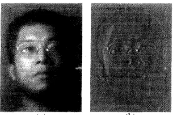
performance can be achieved.Fig, 6 . Images captured by the chip operated in (a) intra frame mode and
(b) frame difference mode.
Fig. 7 shows the readout voltage of the pixel circuit versus the incident photon energy. As shown in the figure, the saturation voltage is 820mV and the sensitivity is 0.2V/luxs
0.9 0.8 0.7 0.6 0.5 > 5 0.4 0 0.3 0
z
m m=
0.2 0.1 0 0 1 2 3 4 5 5 7 8Photon Energy (lux's)
Fig. 7. The photon response of the APS sensor circuit. Fig. 5. APS sensor array structure
Experimental Results
The APS camera chip is fabricated in a 0.5pm double poly double metal CMOS process. The dimension of a sepsor cell is 32.2pm by 32.2pm with a fill factor of 33%. The power supply voltage is 3.3V. The power consumption of
the whole chip is 56mW when operated at 30 frames per second. We built a PC interface card for the camera chip so
the image can be shown on the screen in real time or stored
in the computer for further analysis.
Two sample images captured by our chip are shown in Fig. 6. Fig. 6(a) shows the image captured in intra frame mode, the image quality is good and no observable FPlV is presented. Fig. 6(b).shows the image captured in frame difference mode, only the moving part of the scene appears in the image and the signal values are zero in the stationary hackground area.
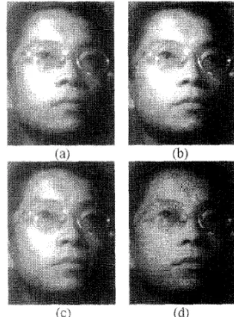
Our sensor cell circuit can provide the frame difference output because the previous frame data are stored in each pixel circuit. If the leakage current associated with the drain region of the shutter switch affects the stored image, the frame difference output can be erroneous. In order to evaluate the effect of leakage current, we use a special operating mode to repeatedly read out an image held in the sensor array. The results are shown in Fig. 8. Fig.
8(a)
shows the original image while Fig. 8(b), (c), and (d) show the output images after I second, 10 seconds, and 1 minute, respectively. The image quality degrades with time as shown in the figures, however, the degradation is not observable within a few seconds.We use the peak signal-to-noise ration (PSNR) to measure the degradation of the image quality held in the sensor array. Fig. 9 shows the PSNR of the image versus time. As shown in the figure, the PSNR is over 40dB when the hold time of the image is less than 4 seconds. In real applications, the hold time is less than 66ms if the frame rate is 3Ofps, so the image degradation is negligible and the frame difference is very accurate.
13.2.3
Fig. 8. Leakage induced quality degradation of image held i n the sensor
a m y with different hold time: (a) the original image, (b) 1 second, (c) 10
seconds, and (d) 1 minute.
45 4 0
-
m p 35 K $ 30 n 25 20 ConclusionA 128x96 pixel CMOS APS camera chip with direct frame difference output is described. We proposed a new cell circuit with in-pixel storage to obtain the frame difference. Each pixel occupies 32.2pmx32.2pm with a fill factor of 33% in a OSpm double poly double metal CMOS process. This cell circuit is optimized for low voltage operation. The power consumption of the sensor chip is 56mW at 3.3V power supply including the on-chip ADC dissipation. From the experimental results, good quality intra frame images and accurate frame difference can be obtained. This chip is suitable for video-oriented applications such as video compression, motion detection, and moving object segmentation systems.
1 5 I
1 10 100
Hold Time (s)
Fig. 10. Die photo of the APS camera chip. References
Fig. 9. Image quality degradation versus hold time.
The die photo of‘ our APS camera chip is shown in Fig. 10.
The chip area including pads is 5.8mmx5.2mm. The features of’ this chip are summarized in Table I.
TABLE I
FEATURES OF THE APS CAMERA CHIP. Technology Chip size Pixel size Power consumption Fill factor Saturation level Sensitivity FPN Power supply 0.5pn DPDM 5.81nm x S.2mm 32.2gm x 32.2~11 3.3V S6mW 3 3 8 8201nV 0.2V/lux*s 8mV
E. R . Fossum, “CMOS image sensors: Electronic camera-on-a- chip,” IEEE TrLmsuctions on Electron Devices, vol. 44, pp. 1689-
1698, Oct. 1997.
A. Dickinson, B. Ackland, E. -S. Eid, D. Inglis, and E. R. Fossum, “A 256x256 CMOS active pixel image sensor with motion detection,” in Proceedings of IEEE Ititernutionul solid-stute Circuits Conference, pp. 226-227, 1995.
R. H. Nixon, S. E. Kemeny, C. 0. Staller, and E. R. Fossum,
“256x256 CMOS active pixel sensor camera-on-a-chip,” in
Proceedings of IEEE /nternationul Solid-Stute Circuits Conference,
S. H. Lewis, H. S. Fetterman, J. George, F. Gross, R.
Ramachandran, and T. R . Viswanathan, “A 10-b 20-Msample/s analog-to-digital converter,” IEEE Journul of’ Solid-Stute Circuits,
vol. 27, pp. 351-358, Mar. 1992.
T. B. Cho and P. R. Gray, “A lob, 20Msample/s, 35mW pipeline
AID converter,” IEEE Journul of Solid-Stute Circuits, vol. 30, pp. 166-172, Mar. 1995.
S. K. Mendis, S. E. Kemeny, R. C. Gee, B. Pain, C. 0. Staller, Q. Kim, and E. R . Fossum, “CMOS active pixel image sensors for
highly integrated imaging systems,” IEEE JOUI%Ul of Solid-Stute Circuits, vol. 32, pp. 187-197, Feb. 1997.
pp. 178-179, 1996.