國
立
交
通
大
學
資訊工程系
碩
士
論
文
針對一個固定集合的應用設計一個
有效減少線路面積的可重組式硬體
DESIGINING A WIRING AREA-EFFICIENT RECONFIGURABLE
HARDWARE FOR A FIXED SET OF APPLICATIONS
研 究 生:盧惠真
指導教授:鍾崇斌 博士
針對一個固定集合的應用設計一個
有效減少線路面積的可重組式硬體
DESIGINING A WIRING AREA-EFFICIENT RECONFIGURABLE
HARDWARE FOR A FIXED SET OF APPLICATIONS
研 究 生:盧惠真
Student:Hui-Zhen Lu
指導教授:鍾崇斌
Advisor:Dr. Chung-Ping Chung
國 立 交 通 大 學
資 訊 工程 學 系
碩 士 論 文
A Thesis
Submitted to Department of Computer Science and Information Engineering College of Electrical Engineering and Computer Science
National Chiao Tung University in partial Fulfillment of the Requirements
for the Degree of Master
in
Computer Science and Information Engineering September 2005
Hsinchu, Taiwan, Republic of China
針對一個固定集合的應用設計一個有效
減少線路面積的可重組式硬體
學生:盧惠真 指導教授:鍾崇斌 博士 國立交通大學資訊工程學系碩士班摘要
可重組式硬體不但提供了利用硬體加速的效能,也同時保留軟體使用的彈性,在 市面上有一種稱作 FPGA(可程式化邏輯陣列)的產品就是此種硬體的先驅者,其已 廣泛使用在 I/C 產品的雛型驗證中。目前 FPGA 的發展趨勢在於使用較多的運算單元來 達成大量的運算,為了因應運算單元的增加,必須提高繞線的能力,因此 FPGA 上會 有許多的稱為繞線元件線和電閘,高度的繞線能力需求將使得 FPGA 大部分的硬體面 積被繞線元件所佔用。 本篇論文的目的在於提供運算最大平行度的前提下,尋求所需盡量小的繞線面 積。藉由針對特定領域的應用來設計可重組式硬體,如此一來祇需要有限度的繞線能 力,自然減少對於繞線元件的需求;因此本論文的重點在於提出減少繞線面積的演算 法。我們從特定領域的應用中,選出值得以可重組式硬體加速的迴圈,並將它們轉換 成資料流程圖,找出資料流程圖以可重組式硬體來實現時,需要用到哪些運算單元和 繞線元件。這個步驟稱為 Placement and Routing,一般的做法是先配置資料流程圖上所 有的運算應該用可重組式硬體上哪個運算單元實現,之後再找出運算跟運算之間的資 料傳送路徑在可重組式硬體上的繞線路徑。這樣的做法使得繞線時的路徑會受限於出 發點和到達點的位置,雖然繞線快速,但不見得有效減少繞線面積。因此我們所提出 的方法為邊放邊繞,在放置每一個運算到可重組式硬體上時,同時考慮如何繞出資料 傳送路徑所增加的繞線面積最小,這個步驟的繞線是已知出發點位置,找出到達點對 應的運算單元及繞線路徑,使得所需增加的繞線面積最小。我們採用了貪婪演算法, 每次找出目前所需最小繞線面積,並以盡量不增加新路線為原則,繞線時優先利用硬 體上已存在的未使用路線片段。基於這個原則,先被選出放置的運算對於後面運算的 放置位置具有影響性,因此運算被選出放置的順序亦在我們考慮之內。實驗結果顯示,我們的方法繞出來的面積比用傳統 VPR(Versatile Placement and Routing)方法繞時少了 28.2%,可以有效降低硬體的成本,當可重組式硬體需求的運 算單元增多時,我們的方法不但可避免因大量的繞線元件需求限制晶片上可容納的運 算單元數量,同時可以減少耗電甚至於因繞線而引起的延遲。
DESIGINING A WIRING
AREA-EFFICIENT RECONFIGURABLE
HARDWARE FOR A FIXED SET OF
APPLICATIONS
Student:Hui-Zhen Lu Advisor:Dr. Chung-Ping Chung Institute of Computer Science and Information Engineering
National Chiao-Tung University
ABSTRACT
The reconfigurable computing offers computation ability in hardware to increase performance, but also keeps the flexibility in software solution. There is a kind of product called FPGA (Field Programmable Gate Array) in the market, which is the harbinger of reconfigurable hardware. It has been common used in IC product verifications. The current developing trend of general FPGAs is to use more processing elements for a large number of computations. For more processing elements, the routability must be increased. Therefore there would be many wires and switches called routing resources in FPGA. High routability demand makes most of the chip area of FPGA used by routing resources.
The purpose of this thesis is to get small wiring area as far as possible and the precondition is to supply the maximal parallelism for computations. By designing our reconfigurable hardware for a fixed set of applications, so only limited routability is needed, and the demand for routing resources is decreased naturally. Therefore the focal point of this thesis is to propose an algorithm of reducing wiring area. From specific applications, we extract loops, which are worth speeding up in reconfigurable hardware. These loops are transferred to data flow graphs, and we must decide what processing elements and routing resources are needed when these data flow graphs are implemented in reconfigurable hardware. This step is called “Placement and Routing”. The general method is first to allocate all nodes in a data flow graph should be implemented by which processing elements in reconfigurable hardware and then to find all edges should be what routing paths in reconfigurable hardware. This kind of method makes routing paths limited by positions of
sources and destinations. Although it is fast, it is not necessarily to reduce wiring area efficiently. So we propose a method of simultaneous placement and routing. While place every node in reconfigurable hardware, simultaneously consider how to route edges to make added wiring area minimal. The routing in this step is that the position of the source is known and to find the processing element for the destination and the routing path to make the added wiring area minimal. We adopt greedy algorithm to find current needed minimal wiring area every time. The principle is not to add new wires as far as possible. The existed non-used wire segments in hardware are used preferentially for routing. On the basis of the principle, the former selected node’s placement would influence the latter node’s placement position. So the order of selected nodes is also one of our considerations.
The simulation results show that the area is fewer by 28.2% when use our method than use traditional VPR (Versatile Placement and Routing). When need processing elements in reconfigurable hardware are increased, to use our method is not only to prevent to limit accommodated processing elements in a chip because of a large number of routing resources and to reduce power consumption even delay comes from routing.
誌 謝
首先我要感謝我的指導老師-鍾崇斌教授,在他的諄諄教誨之下才得以順利完成 此篇論文,同時也要感謝老師這些年來的教導與勉勵,讓我在學業以及待人處世方面 有所精進。 同時也感謝實驗室另一位老師,也是我的口試委員的單智君教授,以及另一位口 試委員陳添福教授,由於他們的指導與建議,讓這篇論文更加的完整和確實。 另外,感謝計算機系統實驗室的學長姐、同學和學弟,真的很高興可以認識你們 大家,因為你們,讓我的研究生活充滿了歡樂,也讓我增廣許多知識和見聞。 還要感謝我的家人以及男朋友,謝謝你們給我的支持與關懷,讓我能無後顧之憂 的學習,讓我追求自己的理想。 最後,所有支持勉勵我的親友及師長們,在此奉上我最誠致的感謝與祝福,謝謝 你們。 盧惠真 2005/9/12 計算機系統實驗室CONTENT
摘要 ... i
ABSTRACT ... ii
誌 謝 ... iv
CONTENT ... v
List of Figures ... vii
List of Tables...viii
CHAPTER 1 INTRODUCTION ... 1
1.1 .The current situation ... 2
1.2 Motivations ... 2
1.3 Objective and Proposed approach ... 3
1.4 Organization of This Thesis... 3
CHAPTER 2 BACKGROUND AND RELATED WORK... 4
2.1Background: Features of FPGA... 4
2.2 Related work: Simulated Annealing Placement ... 6
2.3 Related work: Basic Routing Algorithms ... 8
2.3.1 Maze routing [5]... 9
2.3.2 Rip-Up and Re-Route Algorithm and Multi-Iteration Algorithm ... 10
2.4 Related work: Versatile Place and Route (VPR) tool [3][5] ... 11
2.4.1 Placement algorithm... 11 2.4.2 Routing algorithm... 12
CHAPTER 3 DESIGN ... 16
3.1 Problem Descriptions ... 16 3.2 Basic Ideas... 17 3.3 Hardware Assumptions ... 183.4 The Main Work in Our Design ... 19
3.5 Order Decision ... 21
3.6 Placement and Routing Design ... 23
3.6.1 Undirected routing graph... 23
3.6.2 Routing requirement ... 24
CHAPTER 4 SIMULATION ENVIRONMENT AND SIMULATION
RESULTS... 32
4.1 Benchmark Suite ... 32
4.1.1 Criteria for Selecting Benchmarks ... 32
4.1.2 MediaBench Benchmarks ... 33
4.2 Evaluation... 35
4.3 Simulation Results ... 37
4.3.1 Loop Order ... 37
4.3.2 nodes order ... 37
4.3.3 Compare results with VPR ... 38
CHAPTER 5 CONCLUSIONS AND FUTURE WORK ... 40
List of Figures
Figure 2-1 FPGA Structure... 6
Table 2-1 Schedule table [3] ... 8
Figure 2-2 Maze router examples ... 10
Figure 2-3 Examples of correction factors [5] ... 12
Table 2-2 Correction factors for nets with up to fifty terminals [5].. 12
Figure 3-1 the reconfigurable hardware of our design... 19
Figure 3-2 the flow chart of our main work ... 21
Figure 3-3 example of node’s order ... 22
Figure 3-4 the undirected routing graph ... 24
Figure 4-1 chip area before and after placement and routing... 36
Figure 4-2 results of “with I/O limit” ... 38
Figure 4-3 results of “without I/O limit” ... 38
List of Tables
Table 2-1 Schedule table [3] ... 8
Table 2-2 Correction factors for nets with up to fifty terminals [5].. 12
CHAPTER 1 INTRODUCTION
There are two primary methods in conventional computing for the execution of algorithms [7]. The first is to use hardwired technology, such as Application Specific Integrated Circuit (ASIC). ASICs are designed specifically to perform a given computation for which they were designed. However, the circuit cannot be altered after fabrication. This forces a redesign and re-fabrication of the chip if any part of its circuit required modification.
The second method is to use software-programmed microprocessors—a far more flexible solution. Processors execute a set of instructions to perform a computation. By changing the software instructions, the functionality of the system is altered without changing the hardware. However, the downside of this flexibility is that the performance can suffer, if not in clock speed then in work rate, and is far below that of an ASIC.
Reconfigurable computing is intended to fill the gap between hardware and software, achieving potentially much higher performance than software, while maintaining a higher level of flexibility than hardware.
The most common used reconfigurable hardware is FPGA. An FPGA contain an array of computational elements whose functionality is determined through multiple programmable configuration bits. These elements, sometimes known as configurable logic blocks or logic blocks, are connected using a set of routing resources that are also programmable. Routing resources include wires and switches. The routability of an FPGA depends on the number of wires and switches.
1.1 .The current situation
The developing trend of general FPGAs is to use more logic blocks for a large number of computations [1]. In order to use the same hardware to complete all kinds of computations, there must be very high routability in the hardware. In the other word, there are many wires and switches in the chip. These wires and switches will make the chip area very large. When different computations are completed in the hardware, some wiring area will be idle.
Although the technology grows fast, a chip could contain much more logic blocks. However, the need for high routability makes most chip area is used in routing resource (often 80-90%)[2].
1.2 Motivations
Because high routability comes at a large expense in interconnect costs, we will devise our reconfigurable hardware for some special area applications. By limiting the range of computations in the reconfigurable hardware, we can lower the needed routability.
The multimedia applications are very popular in the market. When we apply them in the reconfigurable hardware, on the one hand we can speed up the intensive computations of multimedia applications and on the other we can lower the cost by employing the same hardware to complete different multimedia applications.
According as integration technologies grow fast, the size of logic blocks will be smaller than before. However, the amount of interconnections will not decrease much. And the chip area will be limited because of many interconnections in the hardware. If we can efficiently arrange wires position, the wiring area will be reduced much more.
1.3 Objective and Proposed approach
The objective of this thesis is to reduce the needed wiring area in the reconfigurable hardware, and the prerequisite is to fix the amount of the logic blocks to keep performance. We will design a reconfigurable hardware from a given logic block array (just like FPGA), and develop a set mechanism to decide the minimal wiring area to complete all need computations selected from multimedia applications. To achieve this objective, we first need to analyze the multimedia applications. Intensive computations will be selected to process on the reconfigurable hardware. We will consider these computations as dataflow graphs, and we must determine how to accomplish these dataflow graphs on the logic block array. This step is called “placement and routing”. By placement, every node in a data flow graph will be decided to use which logic block to complete its computation. By routing, every edge in a data flow graph will be decided to use which routing resources. Good placement and routing makes the needed wiring area reduced.
1.4 Organization of This Thesis
The organization of this thesis is as follows: In Chapter 2, the background and related work are presented. In Chapter 3, the design idea and placement and routing algorithms are described. In Chapter 4, our experimental results and related analysis are presented. Finally, conclusions and future work are presented in Chapter 5.
CHAPTER 2 BACKGROUND
AND RELATED WORK
In this chapter, we will describe the FPGA features and present placement and routing algorithms.
2.1Background: Features of FPGA
Most commercial FPGA architectures have the same basic structure, a two-dimensional array of programmable logic blocks, that can implement a variety of logic functions, surrounded by channels of track segments to interconnect logic block I/O. Three main classes of FPGA architecture have evolved over the past decade: cell-based FPGA architectures, hierarchical architectures, and island-style FPGA. The features of them are listed as follow. 1. Cell-based FPGA
A. Consist of a two-dimensional array of simple logic blocks which contain two or three two-input logic structures such as XOR, AND, and NAND gates
B. Inter-logic block communication: directed wired connections from logic block outputs to inputs on adjacent logic blocks
C. Small numbers of wire segments that span multiple logic blocks offer a minimal amount of global communication but typically not enough to implement circuits with randomized communication patterns.
D. Theses routing restrictions frequently limit the application domain of these devices to circuits with primarily nearest-neighbor connectivity such as bit-serial arithmetic units and regular 2-D filter arrays.
2. Hierarchical architectures
A. Contain a 2-D array of complex logic blocks with many LUTs and flip-flops per logic block (8 or more)
B. Inter-logic block signals are carried on wire segments that span the entire device providing numerous high-speed paths between device I/O and internal logic blocks C. Lead to an ideal implementation setting for designs with many high-fanout signals D. Effectively be used to implement many types of logic circuits exhibiting a variety of
interconnection patterns. 3. Island-style FPGA
A. This style is between cell-based and hierarchical architectures and characterized by logic blocks of moderate complexity generally containing a small number of LUTs B. Routing channels with a range of wire segment lengths are available to support both
local and global device routing
C. Contain a square array of logic blocks embedded in a uniform mesh of routing resources.
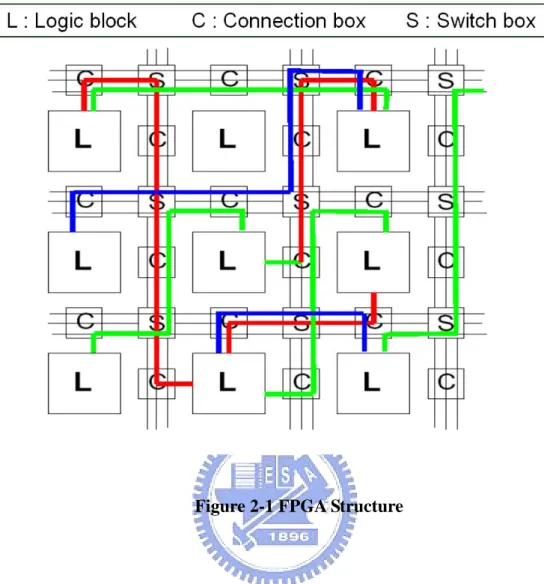
Generally to speak, a common FPGA structure is as Figure 2-1, the logic blocks are embedded in a general routing structure. Given a logic block array, the space between columns or rows is channel. A channel contains some tracks for programmable routing. The channel capacity means the amount of tracks in the channel.
Figure 2-1 FPGA Structure
2.2 Related work: Simulated Annealing Placement
The simulated annealing placement is easier to add new optimization goals or constrains than min-cut and analytic placer and it is the most common iterative technique for island-style FPGAs (and for many other design problems) [4]. It starts with a feasible placement, created either through random assignment of design logic blocks to physical logic blocks, or through the use of constructive approaches and then repeatedly generates placement perturbations in the form of logic blocks swaps. While it clearly makes sense to greedily accept perturbations that reduce overall cost, the search aspect that makes simulated annealing unique is its treatment of swaps that increase or have no effect on overall cost. To avoid local cost minima, there is a need for simulated annealing to occasionally accept logic block swaps that increase
overall cost. By accepting these moves, the global placement can be moved away from a local minimum enhancing the prospect that further cost-reducing swaps may find a more optimal final placement.
An important aspect of the simulated annealing algorithm is the determination of how frequently cost-increasing swaps are accepted. For most algorithms, this acceptance rate is
determined based on a probability, T t
e cos ∆ −
, where ∆costis the swap cost increase and T is the
temperature, a probability parameter which directly controls the acceptance rate. A common
cost function is the sum over all nets of the half-perimeter of their bounding boxes. Initially, T is set to a high value so that almost all swaps, good and bad, are accepted. During progression of the algorithm, T is repeatedly reduced and fewer higher cost permutations are accepted, thus allowing convergence to a final result. Important factors that effect the run time and quality of simulated annealing algorithms are the determination of starting temperature T, adjustment of T, number of permutations attempted at each T, and the ending criteria for the algorithm.
In [4], the pseudo code is as follows.
T = Starting()
Moves per iter = MovesPerIter() While (StoppingCriterion(T) == FALSE) Move count = 0
While (Move count < Moves per iter) Swap blocks
Evaluate ∆cost If ∆cost< 0 Accept swap
Else if (random(0, 1) < T t e cos ∆ − ) Accept swap
Else Reject swap Move count++ EndWhile
T = Adjust(T)
The initial annealing temperature is set to 20 times the standard deviation of the for performing N
cost
∆ blocks random pair-wise swaps. The temperature(T) is updated
according to the follow schedule table so that Tnew=αTold. The ideal commended default
number of moves at each temperature is . Annealing is terminated when T is less
than 3 / 4 blocks N 10 nets N Cost × 005 . 0 . 0.8 Raccept≤ 0.15 0.95 0.15 < Raccept≤ 0.8 0.9 0.8 < Raccept≤0.96 0.5 Raccept> 0.96 α
Fraction of moves accepted Raccept
Table 2-1 Schedule table [3]
2.3 Related work: Basic Routing Algorithms
In this section, we describe the basic maze routing algorithm, the rip-up and re-route algorithm, and the multi-iteration algorithm, which are the basic for many of routing algorithms. By far the most popular routing algorithms for FPGAs are maze-routing algorithms based on Dijkstra’s shortest path algorithm. The routing search starts at a net source and is followed by an iterative evaluation of track segments, based on segment cost, in an effort to avoid congested resources. If all net routed are not initially successful, selected nets are ripped-up and rerouted in an effort to free contested resources.
2.3.1 Maze routing [5]
The maze routing algorithm was designed to find the shortest path between two points on a rectangular grid by using a breadth-first search. The algorithm is guaranteed to find a path, if one exists. When applied to an FPGA, the maze routing algorithm starts at the source node of a net and expands each neighboring node. Expansions continue until the sink node of the net is reached, or all nodes have been visited and no path has been found. However the biggest weakness is very slow. So two main improvements were developed.
1. Depth-first search
Rubin showed that using a depth-first search could significantly reduce the run-time, while still finding the shortest path between two nodes []. For a two-terminal net, choosing a terminal located closer to one of the four corners of the rectangular grid helps to reduce the run-time since the edges of the grid impose boundaries on the search.
2. Directed search
Soukup altered the basic algorithm to make it expand nodes that were successively closer to the sink of a net, creating a directed search algorithm. This algorithm provides an order of magnitude speedup over the basic maze routing algorithm.
The Figure 2-2 shows examples of breadth-first search maze router and directed search maze router. The source of the net is marked with an “S” and the target sink is marked with a “T”. The black squares mark blocked nodes or congestion. The directed search expands significantly fewer nodes than the breadth-first search, since the search expands directly towards the target sink. If there is a significant amount of congestion, the directed search may end up expanding most of the nodes to find a path to the target sink. In the worst case, the
Figure 2-2 Maze router examples [5]
2.3.2 Rip-Up and Re-Route Algorithm and Multi-Iteration Algorithm
Since the routing resources in an FPGA are limited, routing algorithms face the problem of routing congestion. The problem is that routing one net using particular resources may make it impossible to route some other nets. There have been two types of algorithms to deal with the congestion problem [5]. The first type of algorithm is known as rip-up and re-route, such as the work done by Linsker. Another solution to the congestion problem, know as the multi-iteration approach, was conceived by Nair . The main features are as follows.
1. Rip-Up and Re-Route Algorithm
Nets using resources that are congested are ripped-up and re-routed
The success is dependent on the choice of which nets to rip-up and the order in which ripped-up nets are re-routed
2. Multi-iteration algorithm
A routing iteration is the ripping-up and re-routing of every single net
Each net is ripped-up and separately (leaving all the other in place) and re-routed Nets are routed in the same order, but only one net is ripped-up at a time
Nair’s technique is very effective, because nets in non-congested areas can also be relocated to allow nets using congested resources to be routed more easily.
2.4 Related work: Versatile Place and Route (VPR) tool [3][5]
Many placement and routing tools use the basic algorithms in section 2.2 and section 2.3 for their implementation goals, such as to minimize the required wiring length (wire-length-driven), to balance the wiring density across the FPGA (routability-(wire-length-driven), or to maximize circuit speed (timing-driven). In terms of minimizing routing area, VPR outperforms all published FPGA place and route tools. In this thesis, we will take VPR to compare with our design.
2.4.1 Placement algorithm
VPR uses the simulated annealing algorithm mentioned in section 2.2 for placement. A linear congestion cost function provides the best results in a reasonable computation time. The
In the above formulation, the summatio functional form of this cost function is
n is over all the nets in the circuit. For each net, bbx
] ) ( ) ( ) ( ) ( )[ ( , 1 , C n n bb n C n bb n q Cost y av y N n avx x nets + =
∑
=and bby denote the horizontal and vertical spans of its bounding box, respectively. The q(n) is
correction factor which compensates for the fact that the bounding box wire length model underestimates the wiring necessary to connect nets with more than three terminals. Its value depends on the number of terminals of net n; q is 1 for nets with 3 or fewer terminals, and slowly increases to 2.79 for nets with 50 terminals. For example, a net with just two or three terminals will have a correction factor of 1.0 as shown in Figure 2-3. The crossing count of a
four terminal net is about 1.08, since extra wiring is need to reach the fourth terminal, as shown in Figure 2-3. The correction factors for different fanout nets were determined by creating thousands of Steiner trees for randomly distributed net terminals and averaging the correction factor for each of the different fanout nets. Table 2-2 lists the correction factors for nets with up to fifty terminals. Cav,x(n) and Cav,y(n) are the average channel capacities (in
tracks) in the x and y directions, respectively, over the bounding box of net n. This cost function penalizes placements, which require more routing in areas of the FPGA that have narrower channels.
Figure 2-3 Examples of correction factors [5]
Num. Terminals Correction Factor Num. Terminals Correction Factor
2~3 1.00 15 1.69 4 1.08 20 1.89 5 1.45 25 2.87 6 1.22 30 2.23 7 1.28 35 2.39 8 1.34 40 2.54 9 1.40 45 2.66 10 1.45 50 2.79
Ta e 2-2 Correction factors for nets with up to fifty terminals [5]
VPR’s router is based on the Pathfinder negotiated congestion algorithm. Basically, this algor
bl
2.4.2 Routing algorithm
ithm initially routes each net by the shortest path it can find, regardless of any overuse of wiring segments or logic block pins that may result in route fail. An iteration of the router
consists of sequentially ripping-up and re-routing (by the lowest cost path found) every net in the circuit. The cost of using a routing resource is a function of the current overuse of that resource and any overuse that occurred in prior routing iterations. By gradually increasing the cost of oversubscribed routing resources, the algorithm forces nets with alternative routes to avoid using oversubscribed resources, leaving only the net that most needs a given resource behind.
VPR contains two routers: one router is routability-driven, and the other router is timing-drive
for custo
finder algorithm routes nets using a breadth-first maze routing algorithm. A co
= A(i,j)*d(n) + [1 – A(i,j)] * Cost(n) (2.1)
n. We describe VPR’s routability-driven router because it completely devotes to solve congestion without delay time considering. This is the same with our design. The routability-driven routing algorithm in VPR is very similar to the breadth-first routability-routability-driven Pathfinder algorithm, with a few important changes and enhancements.
The Pathfinder algorithm is based upon Nair’s method of iterative maze routing m integrated circuits. During each iteration, every net is ripped-up and re-routed, in the same order during each iteration. During early iterations, nets are allowed to share routing resources with other nets. As the iterations proceed, the sharing of routing resources is penalized, increasing gradually with each iteration. After a large number of iterations, the nets will negotiate among congested resources to try and find a way to successfully route the circuit, allocating key resources to the nets that need them the most. By re-routing all of the nets during each iteration, nets that do not absolutely require congested routing resources can also be relocated.
The basic Path
st function is applied to each node (routing resource) to try and minimize congestion and the delay of more critical nets. The cost function, C(n), applied to each node n by the maze router is:
A(i,j) is the slack ratio from the source of net i to the jth sink of net i. The congestion cost is calculated as:
Cost(n) = [b(n) + h(n)] * p(n) (2.2)
wher g ode n set to e intr sic delay of node n), h(n) is the
(i,j) to 0 for all nets makes the router mple
n) * p(n) (2.3)
excepti
he present congestion penalty, p(n), is calculated by VPR as:
where , capacity(n) is the maximum
e b(n) is the base cost of usin n ( th in
historical congestion penalty based upon the over-use of node n during previous routing iterations, and p(n) is the present congestion penalty based on the over-use of node n during the current routing iteration. If a connection lies on the critical path, then A(i,j) will equal 1.0, and cost function (2.1) will be weighted completely towards optimizing delay. If a connection lies on a path with a large slack, A(i,j) will approach 0, and the cost function (2.1) will be heavily weighted towards minimizing congestion.
VPR’s routability-driven algorithm sets A
co tely routability-driven. In the other word, cost function (2.1) becomes congestion cost function (2.2). And for avoiding having to normalize b(n) and h(n), the congestion cost function used by VPR is:
Cost(n) = b(n) * h(
VPR sets the bases costs of almost all of the routing resources to 1. the only ons are input pins, which are given a base cost of 0.95. This causes the router to expand any input pins reached first and speeds up the routability-driven router by up to 1.5 to 2 times.
T
p(n) = 1 + max(0, [occupancy(n) + 1-capacity(n)] * pfac)
occupancy is the number of nets presently using node n
number of nets that can legally use node n, and pfac is a value that scales the present
congestion penalty. The present congestion penalty is updated whenever a net is ripped-up and re-routed.
The historical congestion penalty, h(n), is calculated by VPR as:
where i al congestion penalty.
{
1,i 1 1 i h * )] capacity(n (n) [occupancy max(0, h(n)i 1 fac),)
(
n
i=
= −+ − >h
is the iteration number, and hfac is a value that scales the historic
CHAPTER 3 DESIGN
In this chapter, we will introduce the problem description and a brief introduction about our design. Then the assumption of our reconfigurable hardware is given. After all, the detail design will be described.
3.1 Problem Descriptions
About our problem, we give some conditions to be our basic design environment. 1. Given conditions
We extract computation intensive loops from benchmark suites. These computation intensive loops are worth speeding up in reconfigurable hardware. And for the convenience of our design, we use data flow graphs to represent these loops.
Because no loops would be executed at the same time, every time we only need to reconfigure one loop’s circuit in the reconfigurable hardware, and no reconfiguration occurs when a loop is executing.
That means our design will consider a loop’s placement and routing to be a main work. Every loop must run the main work one time to decide its needed circuit in the reconfigurable hardware. After all loops’ placement and routing are completed, the needed wiring area will be decided.
2. Objective
Our objective is to find small wiring area in reconfigurable hardware as far as possible to implement all computation intensive loops.
3.2 Basic Ideas
For general placement and routing tools just like VPR, first, all nodes in a data flow graph will be placed in reconfigurable hardware; then all edges will be routed in reconfigurable hardware. After all nodes positions are decided, the routing paths are almost limited in determinate field. The needed wiring area is almost decided after placement. Routing just devotes to route successfully with little influence on wiring area reducing. But, during routing, routing paths gradually dissipate routing resources; a good routing algorithm without limited by placement should make needed wiring area smaller.
Based upon above-mentioned attitude, our design advances the moment of routing. Different from that all nodes are first placed then all edges are routed, a node and its edges are placed and routed simultaneously. And this node’s position is decided by its edges’ routing to make small wiring area as far as possible.
When we decide to take a node and its edges to be placed and routed simultaneously, we find different nodes’ order would result in different needed wiring area. Because preceding nodes’ positions and edges’ routing paths will influence later nodes’ and edges’ placement and routing, the nodes’ order is one of our discussions.
For finding small wiring area as far as possible to implement all loops, we initial logic block array without tracks in it. After a loop is placed and routed, the needed tracks in the logic block array will be left for next loop to route. In the process of placing and routing a loop, the existed track in the logic block array is given higher precedence than new added track. Just like nodes’ order, different loops’ order make different needed wiring area. The loops’ order also is one of our discussions.
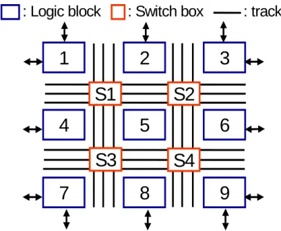
3.3 Hardware Assumptions
We assume our reconfigurable hardware is like Figure 3-1. In our reconfigurable hardware, every logic block is a processing element and every logic block is a square of equal size. Every logic block is responsible for logic functions and easy arithmetic computations such as addition, subtraction, and multiplication. For easy to evaluate the wiring area, a logic block is assigned as a square. Because of the fast growing of integration technologies, we think these assumptions about the logic blocks in our reconfigurable hardware are reasonable.
In order to get detail information of a track (which part is empty or which part is full), the track is split into track segments. A track segment is a part of a track that spans one logic block.
For the I/O pads, we have two independent assumptions. The result of these two different assumptions will be displayed in our simulations. These two different assumptions are as follows:
1. With I/O limit
In this assumption, we assign I/O pins in the logic blocks of the four sides of the logic block array. In order to keep all routing resource for interconnection, we can assign I/O pins in the logic blocks of the four sides of the logic block array. With this assignment, the routing resource can be concerned in interconnection without working for transferring data with CPU and memory. However, the placement will be more limitations. That means the I/O nodes must be placed only in the logic blocks of the four sides of the logic block array.
2. Without I/O limit
We give more flexibility to placement in this assumption. The logic blocks of the four sides of logic block array are still with I/O pins. But the other logic blocks inside the logic block array are given the ability of transferring data with CPU and memory.
However, when these inside logic blocks transfer data with CPU and memory, they must use extra track segments.
We design our reconfigurable hardware as a logic block array. If there are M*N logic blocks in the logic block array, there would be (M-1)+(N-1) channels. Among these channels, there are (M-1) horizontal channels and (N-1) vertical channels. And M*N logic blocks can implement all computation intensive loops selected from multimedia applications.
1
2
3
4
5
6
7
8
9
S3
S1
S2
S4
: Logic block
: Switch box
: track
Figure 3-1 the reconfigurable hardware of our design
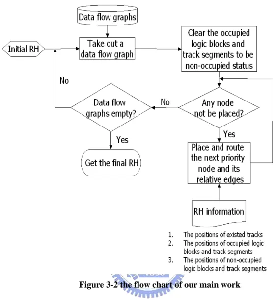
3.4 The Main Work in Our Design
Every time when a data flow graph is selected to place and route in reconfigurable hardware, we use the follow main work to decide how many wiring area is needed to implement this data flow graph.
While there are nodes in the data flow graph not be placed on reconfigurable hardware
1. Select a node u and V= {vi|vi have been placed on reconfigurable hardware
and have edge from or to u}
2. Try to route every (u,vi) to find its suitable routing path which will make
wiring area minimal at the moment, and then to place u on reconfigurable hardware
In this step, vi has been placed in reconfigurable hardware. According to vi’s
position, try to find the best routing path for every (u, vi) which the wiring
area added fewest.
The initial reconfigurable hardware is only a logic block array, and no tracks in it. After a data flow graph is implemented on the reconfigurable hardware, some needed tracks will be added on reconfigurable hardware. When other data flow graph is selected to implement on the reconfigurable hardware, the existed tracks will be given precedence for routing. The Figure 3-2 represents our flow chart.
Figure 3-2 the flow chart of our main work
3.5 Order Decision
We adopt the order dependent method to solve our problem. A good order of placement and routing will take us to a good solution. We divide the order of our problem into two parts as:
1. The loops’ order
The more edges in a data flow graph, the more routing resource needed when placing the nodes and routing the edges in the logic block array. So we can easily decide the order of all loops according to the amount of edges in every data flow graph. A data
edges to place and route in the logic block array. 2. The nodes’ order in a data flow graph
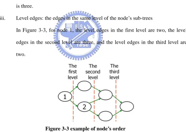
In this part, we apply three evaluations to put the nodes in a dataflow graph in order. Before describe how to decide the priority of nodes, we define these three evaluations as follows.
i. Sub-tree edges: the edges in the sub-trees of a node
In Figure 3-3, the sub-tree edges of node 1 are seven and the sub-tree edges of node 2 are four.
ii. Node degree: the summation of the in-degree and the out-degree of a node In Figure 3-3, the node degree of node 1 is two, and the node degree of node 2 is three.
iii. Level edges: the edges in the same level of the node’s sub-trees
In Figure 3-3, for node 1, the level edges in the first level are two, the level edges in the second level are three, and the level edges in the third level are two.
Figure 3-3 example of node’s order
Three hypothesizes in this thesis are given as follows:
The more a node’s sub-tree edges, the higher its routing resource requirement;
requirement;
The more the closer level edges of a node, the higher its routing resource requirement.
When a node is with higher routing resource requirement, it will be given higher priority. When we can’t use sub-tree edges evaluation select the highest priority node, we apply node-degree evaluation. If the highest priority node still can’t be taken out, the level edges evaluation is used. If still more than one node competes with the highest priority, a random node is selected from the competed nodes. Other priority nodes are selected as above-mentioned.
3.6 Placement and Routing Design
Our design would try to insert routing process into placement. By this method, our design is combined placement and routing. And because the objective is to find small wiring area as far as possible, whenever routing an edge, the existed empty track segments in the reconfigurable hardware would be given higher precedence than to add new tracks in the reconfigurable hardware for routing the edge.
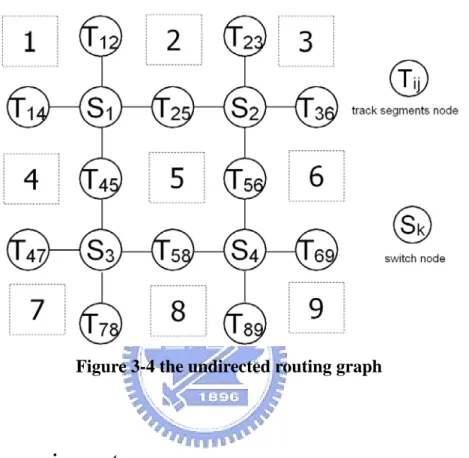
3.6.1 Undirected routing graph
We define an undirected routing graph for placement and routing. In Figure 3-4, we have two kinds of vertices. One kind is Tij and the other is Sk. Tij means a track segments node that
is the set of the track segments that transfer data for the ith logic block or the jth logic block
node, which represents the kth switch box in the reconfigurable hardware. So we can define an
undirected routing graph G(V,E):
V={Tij | data from logic blocki or logic blockj} U{Sk | switch box}E= {(Tij,Sk)| data is transferred between Tij and Sk}
Figure 3-4 the undirected routing graph
3.6.2 Routing requirement
When we try to route an edge e in a data flow graph, we may get many possible routing paths. In this moment, the best routing path for e must be decided. So we apply the three evaluations as follows.
i. The fewest added tracks: ii. The minimal added chip area iii. The shortest routing path
When more than one routing path can route e:
(2) If more than one routing path is possible, then we select the routing path which chip are added the fewest from (1).
(3) If more than one routing path is possible, then we select the routing path that is the shortest from (2).
(4) If more than one routing path is possible, then we randomly select a routing path from (3).
3.6.3 Detail placement and routing design
When we select a non-placed node u and a node set V= {vi | vi have been placed on
reconfigurable hardware and have edge from or to u}, first we can classify u according to whether u is an I/O node that means u needs to transfer data with CPU or memory. Because we have two different assumptions for I/O node placement, classification of u is necessary. Further we can classify V according to the number of elements in V. When u is not an I/O node, we describe in CASE I. When u is an I/O node, it is described in CASE II. And classification of V will be both described in CASE I and CASE II.
CASE I: u is a non-I/O node
We describe different methods for different classifications of node set V according to its number of elements as follows. CASE I.1 describes the situation of one element in node set V, and CASE I.2 describes that of more than one element in node set V.
CASE I.1: Only one element in node set V={v}, v’s position on reconfigurable hardware is
the source of the routing path for (u,v).
fewer added tracks, routing paths with more added tracks would not be found out. Because routing paths with fewer routing requirement have been found, it is unnecessary to find routing paths with more routing requirement. The follow four steps are detail method for
CASE I.1 to route (u,v) and to place u on reconfigurable hardware.
Step I.1.1: no track added
Use maze routing as mentioned in section 2.3.1, limit no track can be added, and routing should be stop in the first empty logic block. In the process, find all possible routing paths, and the end of any one routing path must be an empty logic block for u to be a possible position.
Step I.1.2: If no routing path found in Step1.1, add one track
Use maze routing, limit only one track can be added, and stop in the first empty logic block. In the process, find all possible routing paths, and the end of any one routing path must be an empty logic block for u to be a possible position.
Step I.1.3: If no routing path selected in Step1.1 and Step1.2, add two tracks
Use maze routing, allow two tracks can be added, and stop in the first empty logic block. In this step, to add two tracks to find all possible routing paths is the worst case, because a vertical track and a horizontal track would lead a source of a routing path to any destination. In the process, find all possible routing paths, and the end of any one routing path must be an empty logic block for u to be a possible position.
Step I.1.4: Place u
For the end of the selected routing path, the upper empty logic block has higher priority than the empty lower logic block, and the left empty logic block have higher priority than the right empty logic block. Select the highest priority empty logic block to place u.
CASE I.2: Multiple elements in node set V={vi| vi have been placed on reconfigurable
hardware and have edge from or to u}, and apply ei=(u,vi).
In this case, there exists more than one source must reach the same destination. In the other word, more than one edge must be assigned its suitable routing path that make u have a unique position and the wiring area added fewest in this case. If every ei is assigned a routing path with the minimal routing requirement, there may exist many positions for u. We continue to use method in CASE I.1, but route to the farthest possible empty logic blocks to give more routing paths for every ei. From these routing paths, select suitable routing path for every ei to
find the unique position to place u. The follow steps are detail method for CASE I.2 to route every (u,vi) and to place u on reconfigurable hardware.Step I.2.1: Route every ei base on the
routing method in the CASE I.1, but the farthest possible empty logic blocks is the routing end. Every empty logic block in the scope of possible routing paths would be put in candidate seti
Step I.2.2: find the intersection set of candidate sets
CASE I.2.1: the intersection is not empty
In the intersection set, select the logic block, which have the shortest distance with every vi to place u.
CASE I.2.2: the intersection is empty
Step I.2.2.1: Find the logic block (lb1) that exists at most candidate sets, and apply . Then try to place u at lb1 and route e
i 1
1 candidateset ~candidateset
lb ∈ i+1 ~ en.
Step I.2.2.2: On reconfigurable hardware, find the logic block (lb2) which have the
shortest distance with every vi . Then try to place u at lb2, and route every e I
Step I.2.2.3: compare the routing requirements of step I.1.2.1and step I.2.2.2
if routing requirement of step I.1.2.1 < routing requirement of step I.2.2.2 then place u at lb1
CASE II: u is an I/O node
In hardware assumption, we have two different assumptions in connection with I/O pins. These two different assumptions influence the placement of node u when no element in V. We describe two different placements for u as follows.
Assumption 1 Without I/O limit: Any logic block can transfer data with CPU and memory
In this assumption, we find two different cases:
Case 1 is that empty logic blocks exist in the four sides of the reconfigurable hardware,
whether u can be placed on any one of these empty logic blocks with/out tracked added will be described.
Case 2 is that no empty logic blocks exist in the four sides of the reconfigurable
hardware; whether replace and reroute preceding nodes and edges to make smaller wiring area will be described.
Case 1: try to place u on the empty logic blocks in the four sides of the
reconfigurable hardware
That will be two situations happened. One is Case 1.1: no track added. The other is Case
1.2: tracks must be added, and reroute may be used to reduce new added tracks. These
situations are described as follows.
Case 1.1: no track added when try route
We use routing methods of CASE I to try route (u,v) or every (u,vi) and limit u to be
placed on empty logic blocks in the four sides of the reconfigurable hardware. If no track added when try route, this will be the best situation for u with I/O need with CPU r memory. Because it is unnecessary for u to use extra track segments to transfer data with
CPU or memory. So we can place u on the empty logic block in the four sides of the reconfigurable hardware with the minimal routing requirement to route (u,v) or every (u,vi).
Case 1.2: track added when try route
In this situation, we want to find whether u can be placed on the empty inside logic blocks of the reconfigurable hardware and no new track added when route (u,v) or every (u,vi) using methods of CASE I . If not, preceding routing paths around empty logic
blocks in the four sides of the reconfigurable hardware may be reroute. The rerouting is try to make u can be placed on an empty logic block in the four sides of the reconfigurable hardware and (u,v) or every (u,vi) can be routed with fewer routing
requirement. The follow steps are detail method description.
Step 1.2.1: try route to find the routing path (rp1) with the minimal routing requirement (try to place u on empty logic blocks in the four sides of the reconfigurable hardware)
Step 1.2.2: try to place in the empty inside logic blocks of the reconfigurable hardware then try route to find the routing path (rp2) with the minimal routing requirement
If no area added, use rp2 to route and place the I/O node If area added:
Try to reroute the routing paths around the empty logic blocks of the four sides of the reconfigurable hardware to try route to find the routing path (rp3) with the minimal routing requirement for the I/O node’s in/out edge
If no area added, use rp3 to route and place the I/O node
Case 2: no empty logic blocks in the four sides of the reconfigurable hardware
In this case, we first try to place u on empty inside logic blocks of the reconfigurable hardware and route (u,v) or every (u,vi) to get routing paths with minimal routing
requirement. Then we try to backtrack the data flow graph, to find a node (non-I/O node), which have placed on the logic block in the four sides of the reconfigurable hardware. To see whether the routing requirement can be fewer than place u on empty inside logic blocks of the reconfigurable hardware and route (u,v) or every (u,vi), after backtrack to
release a logic block for u to place. The detail steps are as follows.
Step 2.1: try to place the I/O node in the inside empty logic blocks of the reconfigurable hardware then try route to find the routing paths with the minimal routing requirement Step 2.2: backtrack the data flow graph to replace and reroute
Backtrack to the placed non-I/O node, which are placed on the logic block in the four sides of the reconfigurable hardware
Try to release the occupied logic block to place u and rip up the non-I/O node’s edges’ routing paths.
Replace the node’s position and reroute the edgesFind a replaced node that the area will be added minimal after replaced and reroute and place u and route u or every (u,vi)
Step 2.3: compare the routing path in Step 2.1 and Step 2.2, accept the routing path with less routing requirement then place the I/O node
Assumption 2 With I/O limit: Limit the logic blocks in the four sides of reconfigurable hardware for I/O
In this assumption, when an I/O node is selected to place on the reconfigurable hardware, its possible position will be limit on the empty logic blocks in the four sides of the reconfigurable hardware. And behind this limitation, we use the routing methods in CASE I to route (u,v) or every (u,vi). Non-I/O node still can be placed on any logic
blocks, so these non-I/O nodes may exhaust the logic blocks in the four sides of the reconfigurable hardware. In this situation, we assign an initial placement for roots of a data flow graph before main placement and routing to prevent that non-I/O nodes exhaust the logic blocks in the four sides of the reconfigurable hardware
The first row of the logic block array work is assigned to roots. The initial placement for roots is as follows.
Step1: Allocate the first row of the logic block array to every root according to its descendants
Sort the roots by its descendants (from more to less)
Sequentially allocate successive logic blocks to every root from left to right of the logic blocks of the first row
CHAPTER 4 SIMULATION
ENVIRONMENT AND
SIMULATION RESULTS
In this chapter, we will describe our simulation environment and show the simulation results. For loop’s order, we will prove give a loop precedence to placement and routing is better. For nodes order, the simulation result of three evaluations mentioned in section 3.5 with six different priorities will tell us which is the best for wiring area. The end, the influence of different limits for I/O nodes will be shown and the best result of our design will compare with VPR.
4.1 Benchmark Suite
In this section, we discuss the criteria for selecting our benchmarks, and describe our benchmark suite.
4.1.1 Criteria for Selecting Benchmarks
The criteria for selecting the benchmarks of our simulation are described as follows: Embedded applications:
Since the reconfigurable system is usually utilized for embedded applications, it is important and practical to choose suitable embedded applications as our benchmarks. For the popular IA (Information Appliance) products recently, most of them are
multimedia and communication applications, such as mpeg1/2 encoder/decoder, code encrypt/decrypt, and gsm mobile communication.
Media processing applications:
The trend toward ubiquitous computing will be fueled by small embedded and portable systems that are able to run multimedia applications for audio, video, image, and graphics processing effectively. The reconfigurable system needed for such devices is actually a merged general-purpose processor and reconfigurable hardware. The challenge is to exploit the effective reconfigurable system implementations from the total execution time standpoint for media processing applications.
According to the criteria described above, we adopt the MediaBench consisting of well-known multimedia and communication applications, such as jpeg, mpeg2, gsm, etc., as our benchmark. We will introduce MediaBench in detail in the next subsection.
4.1.2 MediaBench Benchmarks
MediaBench suite is developed to address the modern embedded multimedia and communication applications. The initial goals of MediaBench are as follows.
Accurately represent the workload of emerging multimedia and communications systems.
Focus on portable applications written in high-level languages, as processor architectures and software developers are moving in this direction.
Precisely establish the benefits of MediaBench compared to existing alternatives, e.g., integer SPEC.
MediaBench is composed of complete applications coded in high-level languages. All of the applications are publicly available, making the suite available to a wider user community. MediaBench 1.0 contains applications culled from available image processing, communications, and DSP applications. We give a description of the current components in MediaBench suite as follows.
JPEG:
JPEG is a standardized compression method for full-color and gray-scale images. JPEG is lossy, meaning that the output image is not exactly identical to the input image. Two applications are derived from the JPEG source code: cjpeg, which does image compression, and djpeg, which does decompression. MPEG:
MPEG2 is the current dominant standard for high-quality digital video transmission. The important computing kernel is a discrete cosine transform for coding and the inverse transform for decoding. The two applications used are mpeg2enc and mpeg2dec for encoding and decoding, respectively. GSM:
European GSM 06.10 is a provisional standard for full-rate speech trans-coding, prI-ETS 300 036, which uses residual pulse excitation/long term prediction coding at 13Kbit/s. GSM 06.10 compresses frames of 160 13-bit samples (8 KHz sampling rate, i.e. a frame rate of 50 KHz) into 260 bits. G.721 Voice Compression:
G.721 refers to the implementations of the CCITT (International Telegraph and Telephone Consultative Committee).
PGP:
PGP uses "message digests" to form signatures. A message digest is a 128-bit cryptographically strong one-way hash function of the message (MD5). To
encrypt data, it uses a block-cipher IDEA (International Data Encryption Algorithm), or RSA for key management and digital signatures.
PEGWIT:
PEGWIT is a program for public key encryption and authentication. It uses an elliptic curve over GF ( ), SHA1 for hashing, and the symmetric block cipher square.
255
2
RASTA:
A program for speech recognition that supports the following techniques: PLP, RASTA, and Jah-RASTA. The technique handles additive noise and spectral distortion simultaneously, by filtering the temporal trajectories of a non-linearly transformed critical band spectrum.
EPIC:
EPIC is an experimental image compression utility. The compression algorithms are based on a bi-orthogonal critically sampled dyadic wavelet decomposition and a combined run-length/Huffman entropy coder. The filters have been designed to allow extremely fast decoding without floating-point hardware.
ADPCM:
Adaptive differential pulse code modulation ADPCM is one of the simplest and oldest forms of audio coding.
4.2 Evaluation
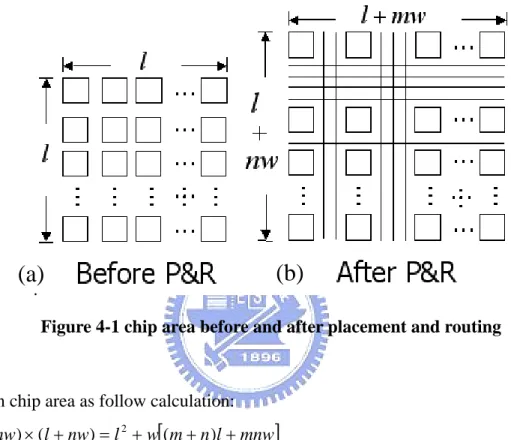
According to a beforehand experiment, we had known that there were 97 nodes in the largest loop. Therefore we design our reconfigure hardware as a 10x10 logic block array for our simulation. For the computation convenience, some assumptions are given. In our experiment, the logic block array is initially no tracks. Gradually, a loop followed a loop will
array before placement and routing is as follow left Figure 4-1(a). We assume the size the initial logic block array is l*l. When some tracks are added the wiring area will be added like Figure 4-1(b). In Figure 4-1(b), m vertical tracks and n horizontal tracks are added. We assume width or length w will be added after a track is added.
.
(b)
(a)
Figure 4-1 chip area before and after placement and routing
Given chip area as follow calculation:
ent which meet our demand such that:
p area (wiring area) after m vertical tracks and n horiz
[
m n l mnw]
w l nw l mw l+ )×( + )= + ( + ) + ( 2And take a determinate processing elem 32 * 2 , 10 * 250λ = λ = w l w l ≈39
λ is the smallest size in a layout. So we can derive the added chi ontal tracks added is:
2 ] ) ( 39 [ m+n +mn w
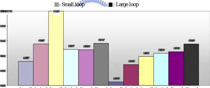
4.3 Simulation Results
der will result in different wiring area. We note subtree edges as s,
4.3.1 Loop Order
From Figure 4-2 and Figure 4-3, we can see two group bars in every figure. These two grou
4.3.2 nodes order
In section 3.5, we set three evaluations to decide nodes order. In this section, we compare diffe
In every figure, different or
node degree as n, level edges as l, and (i,j,k) as priority relation. For example: (s,n,l) means subtree edges priority is higher than node degree and node degree priority is higher than level edge.
ps represent two different loop orders: the one is that give precedence to a loop of fewer edges, and the other is that give precedence to a loop of more edges. From the two figures, we can know that give precedence to a loop of more edges will result in smaller wiring area at the end of placement and routing all loops
rent nodes order from six priorities of the three evaluations. From Figure 4-2 and Figure 4-3, when priority relation is: subtree edge higher than node degree and node degree higher than level edges, the last needed wiring area will be the smallest.
Figure 4-2 results of “with I/O limit”
4.3.3 Compare results
We combine Figure 4-2, Figure 4-3, and VPR result in Figure 4-4. VPR’s best result need 5811 6391 6211 6198 6421 5119 5703 5974 6079 6133 6399 7500 5000 5500 6000 6500 7000 7500area: w^2
: Small loop : Large loop
(s,n,l) (s,l,n) (n,s,l) (n,l,s) (l,s,n) (l,n,s) (s,n,l) (s,l,n) (n,s,l) (n,l,s) (l,s,n) (l,n,s) 6005 6302 6388 6377 6421 5455 5905 6158 6222 6301 6401 7500 5000 5500 6000 6500 7000 7500area:w^2
: Small loop : Large loop
(s,n,l) (s,l,n) (n,s,l) (n,l,s) (l,s,n) (l,n,s) (s,n,l) (s,l,n) (n,s,l) (n,l,s) (l,s,n) (l,n,s)
Figure 4-3 results of “without I/O limit”
with VPR
s 1.282 times our best result, which is no I/O, limit for all nodes. Although our result, which is with I/O limit, needs 1.065 times the best result, but it needs less computation time
because backtrack and reroute are not used.
igure 4-4 compare all res
F ults
Without I/O limit
With I/O limit
(s,n,l) (s,l,n) (n,s,l) (n,l,s) (l,s,n) (l,n,s) (s,n,l) (s,l,n) (n,s,l) (n,l,s) (l,s,n) (l,n,s) VPR 1 1.056 1.162 1.037 1.363 1.086 1.129 1.105 1.127 1.115 1.1671.163 1.465 1.065 1.173 1.153 1.231 1.202 1.247 1.215 1.245 1.231.254 1.25 1.363 1.282 0. 1. 1. 1. 1. 1.
ea/the smallest area : Small loop : Large loop
5 ar 4 3 2 1 1 9
CHAPTER 5
CONCLUSIONS AND FUTURE
WORK
Our design algorithms use no estimation in placement, but give node’s order previously, arrange an order of small area added as far as possible in iterations.
During iteration, we process small area added routing as far as possible to determine placement. Our superiority is that it is easier to get better result from actually saving area of routing to determine placement. When need processing elements in reconfigurable hardware are increased, to use our method is not only to prevent to limit accommodated processing elements in a chip because of a large number of routing resources and to reduce power consumption even delay comes from routing.
But computation time is more than VPR because of exhaustive search for the best routing path. If we can establish a cost function to more efficiently determine the best routing path, the computation time will be lower.
REFERENCE
[1] A. Takahara, T. Miyazaki, T. Miyazaki, T. Murooka, M. Katayama, K. Hayashi, A. Tsutsui, T. Ichimori and K. Fukami, “More Wires and Fewer LUTs: A Design Methodology for FPGAs”, In Proceedings of the 1998 International Symposium on Field
Programmable Gate Arrays, 1998, pp. 12 - 19
[2] André DeHon, “Balancing Interconnect and Computation in a Reconfigurable Computation in a Reconfigurable Computing Array (or, why you don’t really want 100% LUT utilization)”, In Proceedings of the International Symposium on Field
Programmable Gate Arrays, 1999, pp. 125 - 134.
[3] V. Betz and J. Rose, “VPR: A New Packing, Placement and Routing Tool for FPGA Research”, Int. Workshop on Field-Programmable Logic and Applications, 1997, pp. 213 - 222.
[4] V. Betz and J. Rose, Architecture and CAD for Deep-Submicron FPGAs,.Kluwer Academic Publishers, 1999
[5] J. Swartz, “A High Speed Timing-Aware Router for FPGAs”, Master's Thesis, Department of Electrical and Computer Engineering, 1998.
[6] Russel G Tessier, “Fast Place and Route Approaches for FPGAs”, Ph.D. thesis, Department of Electrical. Engineering and Computer Science, MIT, February 1999. [7] K. Compton, S. Hauck, "Reconfigurable Computing: A Survey of Systems and Software",
![Table 2-1 Schedule table [3]](https://thumb-ap.123doks.com/thumbv2/9libinfo/8746382.205072/18.892.120.803.280.713/table-schedule-table.webp)
![Figure 2-2 Maze router examples [5]](https://thumb-ap.123doks.com/thumbv2/9libinfo/8746382.205072/20.892.129.792.157.433/figure-maze-router-examples.webp)
![Figure 2-3 Examples of correction factors [5]](https://thumb-ap.123doks.com/thumbv2/9libinfo/8746382.205072/22.892.135.753.438.904/figure-examples-of-correction-factors.webp)