國
立
交
通
大
學
材料科學與工程學系
博 士 論 文
黃銅礦奈米晶體的合成與光學特性研究
Study on Synthesis and Optical Characteristics of
Chalcopyrite Nanocrystals
研 究 生:郭冠廷
指導教授:陳三元 博士
黃銅礦奈米晶體的合成與光學特性研究
Study on Synthesis and Characteristics of
Chalcopyrite Nanocrystals
研 究 生:郭冠廷 Student:Kuan-Ting Kuo
指導教授:陳三元博士
Advisor : Dr. San-Yuan Chen
國 立 交 通 大 學
材料科學與工程學系
博 士 論 文
A Thesis
Submitted to Department of Materials Science and Engineering
College of Engineering
National Chiao Tung University
in partial Fulfillment of the Requirements
for the Degree of Doctor in
Materials Science and Engineering
August 2009
Hsinchu, Taiwan, Republic of China
黃銅礦奈米晶體的合成與光學特性研究
研究生:郭冠廷 指導教授:陳三元
國立交通大學材料科學與工程學系
中文摘要
銅銦二硫半導體近來被認為是最佳的太陽能材料,因為其具有適合的能帶寬(1.5 eV) 和高吸收係數,與理想的太陽能光譜幾乎完全匹配,若作為太陽能電池的吸 收層可將入射光子完全吸收。過去十年,銅銦二硫薄膜被廣泛研究,其太陽能最 佳轉換效率達到12.7%。此外,銅銦二硫奈米晶體仍被認為具有相當大的潛力可 提高太陽能轉換效率,這是因為奈米晶體產生的量子侷限效應具有多重激子 (multiple excitons)與內部能帶(intra band-gap)的優點。因此本論文將探討銅銦琉 與類銅銦二硫奈米晶體的合成,結構鑑定與在太陽能電池元件的相關應用。 本論文首先利用膠體方法合成銅銦琉的奈米晶體與不同厚度包覆的核-殼結 構的銅銦二硫-硫化鋅奈米晶體,並以 X 光繞射儀(XRD)、穿透式電子顯微鏡 (TEM)、X 光光電子能譜儀(XPS)、動態雷射散射分析儀(DLS)鑑定合成奈米晶 體的結構與粒徑大小。本論文合成的均勻銅銦二硫奈米晶體的粒子半徑為2.4 奈 米,核-殼結構耐米晶體粒子半徑大小則為 4.6 奈米。由於量子侷限效應,所得銅 銦二硫奈米晶體的放射光波長在 450 奈米,明顯高於塊材的銅銦二硫半導體能 帶。硫化鋅表面改質消除了銅銦二硫奈米晶體表面的缺陷,因此可明顯提高其發 光強度。 合成銅銦二硫奈米晶體後,我們將三種不同比例的鋅導入銅銦二硫奈米晶體 中,分別為n=1,n=2和n=3(n=Cu/Zn)。並將這些奈米晶體嫁接到5μm長的氧化 鋅奈米線上,探討其太陽能轉換效率。合成後的鋅參雜銅銦二硫奈米晶體的吸收 波長分別為530(n=1),570(n=2)和650(n=3)奈米。當n=2的時候,可得到最佳的轉 換效率,其值為0.28%,短路電流(Jsc)為1.71mA/cm2,開路電壓(Voc)為0.34V,而填充係數(FF)則為0.48。此類型量子點太陽能電池的限制來自於激子快速的再 結合與電解液,當沉積硫化鋅保護層於鋅參雜銅銦二硫奈米晶體表面後,主要太 陽能電池參數都獲得提升(Jsc = 3.21 ma/cm2, Voc = 0.45 V, FF = 0.49),因此得到 轉換效率為0.71%。
本論文提出的第二個方法是在高頻磁場(High frequency magnetic field)下合 成高品質的鋅參雜的銅銦二硫奈米晶體,所有實驗過程在正常大氣環境與室溫下 即可進行。磁性的參雜提供了主體(host)在外加磁場下產生超順磁性加熱,使得 晶體以高於傳統高溫爐加熱速度的2-3個級數快速成長。隨磁場時間的作用,鋅 參雜的銅銦二硫奈米晶體形貌隨之變化,從球體,錐體,立方體,最後形成長方 體。 本論文最後將磁場下合成的,含有不同形狀銅銦二硫奈米晶體的膠體溶液製 成"奈米墨水"並應用於太陽能電池元件中,將其塗佈成銅銦二硫薄膜吸收層, 最佳轉換效率為1.01%,吸收層膜厚為1.012μm(長方體樣品)。吸收層膜厚提高 到2.132μm後效率可達到1.44%。
Study on Synthesis and Optical Characteristics of Chalcopyrite Nanocrystals
Student : Kuan-Ting Kuo Advisor : San-Yuan Chen
Department of Materials Science and Engineering National Chiao Tung University
Abstract
Copper indium disulfide (CuInS2) semiconductor has been considered as the best materials for solar-cells because it has a superior band-gap of 1.5 eV and high absorption coefficient, which matches almost ideally to the solar spectrum and assures a complete absorption of the incident photon flux in an absorber layer. In the past decade, CuInS2 film has been widely studied and the best conversion efficiency for solar cells is about 12.7 %. On the other hand, CuInS2 nanocrystals still have great potential to promote power conversion efficiency due to quantum confinement effect, such as multiple excitons and intra band-gap. Therefore, in this thesis, the synthesis, characterization and application of CuInS2 and derivative nanocrystals, will be systematically studied.
The bare CuInS2 with different shell thickness, CuInS2@ZnS core-shell nanocrystals, are first produced via a colloidal method and characterized by X-ray diffraction (XRD), transmission electron microscopy (TEM), X-ray photoelectron spectroscopy (XPS), and dynamic light scattering (DLS). The obtained nanocrystals are quasimonodisperse with an average particle size of 2.4 (bare) and 4.6 (core-shell) nm, respectively. The emission peak of obtained CuInS2 is around 450 nm, which is higher than bulk CuInS2 due to the size-dependent quantum confinement effect. ZnS modification eliminates defects on the surface of CuInS2 and significantly enhances photoluminescence consequently.
CuInS2 nanocrystals with three different Cu/Zn ratios (n value) which were and then deposited onto 5 μm long ZnO nanowire substrate as a quantum dot (QD)-based solar cell. The absorbance peak of obtained Zn doped CuInS2 nanocrystals shift from 530, 570, to 650 nm correspond to n = 1, 2, and 3, respectively. The best conversion efficiency of bare Zn doped CuInS2 is0.28 % for n =2 sample, short-circuit current density (Jsc) is 1.71 mA/cm2, open-circuit voltage (Voc) is 0.34 V, and fill factor (FF) is 0.48. It was fond that the restriction of such quantum dot-based solar cells could be due to the fast recombination time and corrosion from electrolyte. But, after depositing ZnS layer on the surface of Zn-CuInS2 nanocrystals, an optimal efficiency at 0.71 % could be obtained, resulting from the promotion of all solar cell parameters. (Jsc = 3.21 ma/cm2, Voc = 0.45 V, FF = 0.49)
The second novel method we present is using magnetic Zn doping to synthesize high quality CuInS2 nanocrystals under high frequency magnetic field at ambient conditions. The magnetic doping gives superparamagnetic heating of the resulting nanocrystals via magnetic induction, causing an accelerating growth rate of the doped CuInS2 under ambient conditions of 2-3 orders of magnitude faster than conventional autoclave synthesis. Shape evolution of the Zn doped CuInS2 nanocrystals from initially spherical, to pyramidal, cubic, and finally to a bar geometry, were detected as a function of time of exposure to magnetic induction.
Finally, these colloidal solvent with different shape nanocrystals were further used as “nanoink” to fabricate a simple thin film solar device, the best efficiency of these crystals we obtained is 1.01 % with a 1.012 um thick absorber layer (bar geometry). The efficiency can be promoted to 1.44 % after thickening absorber to 2.132 um.
Keywords: chalcopyrite, CuInS2, nanocrystal, solar cell, core-shell, high frequency magnetic field.
Ackonwledgements
My greatest debt is to my advisor, Prof. Dr. San-Yuan Chen, who provided me the opportunity to study in his group. Under his discipline, I have been enabled to develop my potential and finish this thesis. Much training he gave me to research independently and think deeply have stimulated my indomitable attitude, and enabled me to accumulate more experiences in my independent work.
I am deeply grateful to Dr. Dean-Mo Liu, whose detailed supervision and continuous supports laid a smooth foundation for my studies. From the experimental work, discussions, to the corrections of this dissertation, especially in editing of the English, he has given essential constructive and indispensable input to this dissertation. His intrinsic carefulness and patience led all my papers and this dissertation to much less errors and more readable.
During my first 4 years, I am particularly thankful for the financial support from Chunghwa Picture Tubes (CPT) Inc and Dr. Bing-Ming Cheng who serves at the National Synchrotron Radiation Research Center (NSRRC). Without their support, I might not able to continue my Ph D study.
I am especially indebted to my colleague in this lab, who contributed directly and indirectly to this accomplishment.
Last, I appriciate my family for their understanding and unconditional support, and thank my friends in “39 group” for their accompanying and listening in my difficult time. Finally, special thanks to my girl friend, Wei-Chen, who gave me the most patient and loving supports, as well as encouragement during the course of this work.
Kuan-Ting Kuo, September 2009 Hsinchu, Taiwan
Contents
中文摘要... i
Abstract... iii
Ackonwledgements ...v
Contents ... vi
Figure captions ... ix
Table captions... xiii
Chapter 1 ...1
Introduction...1
Chapter 2 ...5
Literature Review and Theory ...5
2.1 Development of Solar Cell...5
2.2 Brief Review of CuInS2...12
2.2.1 Crystal Structure of CuInS2...12
2.2.2 Physical Properties...13
2.3 Synthesis Methods of Nanocrystal CuInS2...16
2.3.1 Solvothermal...16 2.3.2 Single-source precursor...17 2.3.3 Hot-Injection ...22
Chapter 3 ...25
Experiment ...25
3.1 Chemicals...25 3.2 Characterization ...253.2.1 Structure and morphology ...25
3.2.2 Optical measurement...26
3.3.3 Solar parameter measurement...26
3.2.4 High frequency magnetic field set up...27
3.3 Material fabrication...27
3.3.1 Synthesis of CuInS2 nanocrystals ...27
3.3.3 Systhesis of ZnO nanowire...28
3.3.4 Synthesis of Zn-CIS quantum dots...28
3.3.5 ZnS coating of Zn-CIS quantum dots ...29
3.3.6 Synthesis of hydrophilic quantum dots by ligand exchange ...29
3.3.7 Assembling Zn-CIS quantum dots on ZnO Nanowires...30
3.3.8 Fabrication of solar cells ...30
3.3.9 Synthesis of Zn-CIS nanocrystals in the presence of high frequency magnetic field ...30
3.3.10 Fabrication of Zn-CIS thin film solar cells...31
Chapter 4 ...32
Synthesis and Characterization of Highly Luminescent CuInS
2and
CuInS
2/ZnS (Core/Shell) Nanocrystals...32
4.1 Introduction...32
4.2 Formation and microstructure of CuInS2...33
4.3 Photoluminescence (PL) of the CuInS2 Nanocrystals...36
4.4 Summary...38
Chapter 5 ...40
Core-Shell CuInS
2/ZnS Quantum Dot Assembled on Short ZnO
Nanowire with Enhanced Photo-Conversion Efficiency...40
5.1 Introduction...40
5.2 Quantized Zn-CIS particles and their deposition on ZnO nanowires ...42
5.3 Photovoltaic performance of the devices with various ratio of Zn dopant.46 5.4 Design of the ZnS shell as a dual-function layer ...50
5.5 Mechanistic aspects of charge transfer into ZnO nanowires...52
5.6 Effect of ZnS shell thickness ...56
5.7 Concluding Remarks ...58
Chapter 6 ...61
Magnetically-induced Synthesis of Highly-Crystalline Ternary
Semiconductor Chalcopyrite Nanocrystals at Ambient Conditions ..61
6.1 Introduction...61
6.2 Optical behavior...63
6.3 Growth of Zn-CIS nanocrystals ...65
6.5 Discussion...72
6.6 Conclusion and implication...81
Chapter 7 ...82
Application of Zn-CuInS2 Nanocrystals Synthesized through
Magnetic Field...82
Chapter 8 ...87
Conclusion ...87
Reference...89
Curriculum Vitae ...107
Publication list...108
Figure captions
Figure 2.1 Mechanism of first generation solar cell....6
Figure 2.2 Schematic cross section of a typical CuInGaSe2 solar cell. ...7
Figure 2.3 Principle of operation and energy level scheme of the dye-sensitized nanocrystalline solar cell. [35]...9
Figure 2.4 Structure of basic quantum dot solar cell. ...9
Figure 2.5 Idealized energy band diagram of a quantum dot solar cell. [8] ...10
Figure 2.6 Enhance photovoltaic efficiency in quantum dot solar cell by impact ionization. [9]...10
Figure 2.7 Schematic device of CdSe QD/ZnO-based DSSC. [37]...11
Figure 2.8 Illustration of CdSe QDs/TiO2-based DSSC. [38] ...11
Figure 2.9 Structures of (a) zincblende ZnS and (b) chalcopyrite CuInS2. ...13
Figure 2.10 Schematic band structure of CuInS2, with indication of contributions of the atomic orbitals and the corresponding energy levels. Shade areas denote the major subbands, and the boxed numbers mark the three internal gaps. [44]...14
Figure 2.11 TEM image of CIS nanorod. [39]...16
Figure 2.12 The dependence of absorption energy on the norminal Se content (mol %) for the samples. [69]...17
Figure 2.13 Molecular structure of (PPh3)2CuIn(SEt)4. [70]...18
Figure 2.14 TEM images of CuInS2 nanocrystals grown at 225 and 250oC. Scale bars in the images are both 5 nm. [73] ...19
Figure 2.15 (a) Absorption, fluorescence emission, and photoluminescent excitation spectra of a typical colloidal solution of CIS nanocrystals. (b) Absorption and fluorescence emission spectra of CIS with hexanethiol, TOPO, and pyridine organic capping ligands (from top to bottom). [73] ...20
Figure 2.16 Effect of different capping agents on the emission intensities of CIS nanocrystals generated from the photolysis. [74] ...21
Figure 2.17 Vials of samples from the irradiation of solution of precursor [(TOP)2CuIn(SR)4] in DOP for (from left to right) 0, 2, 4, 6, 8, 11, 21, 30, 50, 74, 214, and 218 h. [74] ...21
Figure 2.18 Schematic diagram of the energy levels and transitions that have been observed in single-crystal CIS. [73]...22
Figure 2.19 Raw material composition effects on optical properties: (a) UV-vis absorption and (b) PL emission spectra (excitation 500 nm). (Raw material composition Zn:Cu;In:S = 1:n:n:4 (n = 0.5-5).) [75]...23
Figure 4.1 (a)XRD patterns of pure CIS and (b) CIS/ZnS (coe/shell) NCs as well as
CIS. (vertical bars, JCPDS card No. 32-0339). ...34
Figure 4.2 (a)TEM image, and (b) HRTEM image of CIS, as well as (c) HRTEM
image of CIS/ZnS NCs. Particle size distribution histograms of (d) CIS, and (e) CIS/ZnS NCs. ...35
Figure 4.3 XPS of CIS (a) and CIS/ZnS (b) core/shell NCs...36 Figure 4.4 Uv-vis absorption, excitation and PL emission spectras of CIS NCs. The
inset highlights the ultraviolet region spectra showing an increased absorption at higher energies with increasing coverage due to direct
absorption into the ZnS shell. ...37
Figure 4.5 PL emission spectra of CIS and multi-layers ZnS coating on the surface
of CIS NCs. PL emission spectra of pure ZnS and CIS NCs are shown in the inset of the emission spectra. ...38
Figure 5.1 Schemetic diagram of charge transfer from Zn-CIS quantum dot into ZnO
nanowire...42
Figure 5.2 Absorption spectra of Zn-CIS quantum dots with various Cu/Zn ratios from
n=1, n=2, and n=3 in (a) toluene and (b) water. ...44
Figure 5.3 (a) Cross-sectional scanning electron micrograph of ZnO nanowires. (b)
High-resolution transmission electron micrograph of a Zn-CIS quantum dot capped with MPA. (c) Bright-field transmission electron micrograph of a ZnO nanowire decorated with Zn-CIS quantum dots. (d) High-resolution transmission electron micrograph of Zn-CIS quantum dots attached to a ZnO nanowire. Some quantum dots have been outlined. ...45
Figure 5.4 Photographs of different Cu/Zn ratio Zn-CIS quantum dots (a) in toluene,
(b) anchored on ZnO NWs films. (c) Absorption spectra of different Cu/Zn ratios Zn-CIS quantum dots anchored on ZnO nanowires plate...47
Figure 5.5 Current-voltage characteristics of Zn-CIS QDs-DSSC devices with
different n value under stimulated AM 1.5 solar illumination (100 mW/cm2) and active area 0.28 cm2. ...48
Figure 5.6 Current-voltage characteristics of Zn-CIS QDs-DSSC devices fabricated
with (spot) ZnS coating and (square) without. Samples were measured under stimulated AM 1.5 solar illumination (100 mW/cm2) and active area 0.28 cm2. ...51
Figure 5.7 Emission spectra of 4.5 nm (n = 2) diameter Zn-CIS quantum dot film
deposited on (a) glass and (b) ITO/ZnO NWs films. Excitation was at 410 nm. Spectra b carries a multiplication factor of 3. All of the spectra were recorded using front face geometry. ...53
Figure 5.8 Fluorescent decay of 4.5 nm (n=2) diameter Zn-CIS quantum dots deposited
decay of ZnS-coated Zn-CIS quantum dots deposited on ZnO nanowires film...55
Figure 5.9 Current-voltage characteristics of Zn-CIS@ZnS-DSSC devices fabricated
with different monolayer ZnS coating absorber under stimulated AM 1.5 solar illumination (100 mW/cm2) and active area 0.28 cm2. ...57
Figure 5.10 High-resolution transmission electron micrographs of (a) one “bare”
Zn-CIS nanocrystallite and (b) one Zn-CIS nanocrystallite with a 2.5 monolayer ZnS shell. (c) Corresponding XRD patterns for (a) Zn-CIS nanocrystals and (b) ZnS-coated Zn-CIS. Two standard data for ZnS (top inset, vertical bars, JCPDS card No. 05-0566) and CuInS2 (bottom inset, vertical bars, JCPDS card No. 75-0106) are shown for comparison. ...60
Figure 6.1 Apparatus setup for the magnetically-induced synthesis. ...63 Figure 6.2 Absorption (left) and photoluminescence (right) spectra of ZCIS colloids
obtained by HFMF in 30 and 45 seconds. Inset shows the visual image of these two ZCIS colloids under a 365 nm UV lamp irradiation...65
Figure 6.3 UV-vis absorption spectra of Zn-CIS nanocrystals under magnetic exposure
(from left to right: 30, 45, 180, 300, and 420 sec.). ...65
Figure 6.4 HRTEM images of the Zn-CIS nanocrystals with various geometries; (a)
nanoparticle, (b) nanopyramid, (c) nanocube, (d) nanobar synthesized under magnetic exposure. (e) Schematic of the growth of nanoparticles into various geometries of different size, from nanopyramids, nanocubes, and nanobars under magnetic induction. ...67
Figure 6.5 TEM images of samples (a) nanoparticles, (b) nanopyramids, (c)
nanocubes, (d) nanobars. (All the images have the same scale bars (10 nm).) ...68
Figure 6.6 Energy dispersive X-ray spectra (EDX) and corresponding TEM images
of nanobar shaped ZCIS nanocrystals. EDX analysis evidences components of ZCIS nanocrystals. Larger pyramidal shape of ZCIS crystals also found under long-term HFMF exposure, which indicated small pyramidal crystals kept growing along three directions and eventually coexisted with nanorod crystals. ...70
Figure 6.7 XRD patterns of the Zn-CIS nanocrystals of different shapes, with
bottomlines on the x-axis, denoting standard CIS powder diffraction pattern. ...71
Figure 6.8 XRD spectrum of Zn-CIS nanobar by using higher-energy XRD, bottom
inset is the chalcopyrite structure CuInS2 for comparison...72
Figure 6.9 Magnetization curves measured at room temperature for Zn-CIS QDs
the data after subtracting the high-field diamagnetic component...73
Figure 6.10 Magnetization curves measured at different temperature for Zn-CIS QDs.
...73
Figure 6.11 Mechanism of “first paramagnetic nanocrystal” formation...75 Figure 6.12 Magnetization curve of precipitation from Zn and Cu precursors. ...77 Figure 6.13 HR-TEM images of ZCIS nanocrystals synthesized through
high-temperature organic solvent method (a) and HFMF (b). This comparison indicated that crystallinity of ZCIS nanoparticles was
enhanced by HFMF...78
Figure 6.14 Fluorescence (a) and absorption (b) spectra of the Zn-CIS nanocrystals
obtained with (red) and without magnetic induction (black). The excitation wavelength for the fluorescence measurements was 366 nm. ...80
Figure 7.1 Prototype structure of Zn-CIS device. ...83 Figure 7.2 Current-voltage characteristics of Zn-CIS devices with different shape
nanocrystal under stimulated AM 1.5 solar illumination (100 mW/cm2) and active area 0.28 cm2. ...83
Figure 7.3 UV-vis absorption spectra of different shape Zn-CIS nanocrystals. ...85 Figure 7.4 Current-voltage characteristics of Zn-CIS devices with different Zn-CIS
film thickness under stimulated AM 1.5 solar illumination (100 mW/cm2) and active area 0.28 cm2. ...86
Table captions
Table 2.1 Summary of crystal structure, space group, Bravais lattice, and lattice
constants of CuInS2 in the zincblende, chalcopyrite...13
Table 2.2 Summary of the defect levels of donors and acceptors reported for CuInS2. ...15
Table 5.1 Photovoltaic performance of the Zn-CIS/ZnO DSSCs under AM1.5
illumination (Power 100 mW/cm2) and active area 0.28 cm2...50
Table 5.2 Kinetic parameters of Zn-CIS emission decay analysis ...55 Table 5.3 Photovoltaic performance of the Zn-CIS@ZnS/ZnODSSCs under AM1.5
illumination (Power 100 mW/cm2) and active area 0.28 cm2...57
Table 6.1 Composition of the varied structure Zn-CIS nanocrystal...69 Table 6.2 Zeta potential values of different shape Zn-CIS nanocrystals. Particles are the
sample obtained under HFMF duration for 30 and 45 seconds which show emission peaks at 590 and 630 nm. ...79
Table 7.1 Photovoltaic performance of the different shape-Zn-CIS nanocrystal-based
devices under AM 1.5 solar illumination (100 mW/cm2) and active area 0.28 cm2. ...85
Table 7.2 Photovoltaic performance of the different thickness of Zn-CIS nanocrystal
film devices under AM 1.5 solar illumination (100 mW/cm2) and active area 0.28 cm2. ...86
Chapter 1
Introduction
During the past decade, the energy resource concerns have become more and more imperative, great efforts have been focused on the development of renewable energy resources, [1-2] among which photovoltaic solar power holds the great potential and brilliant advantages such as unpollutedness, safety and inexhaustibleness. The development of photovoltaic community is well aware of the cost benefits which associated with the continued increase in solar cell efficiency. Over the past decade much of the cell efficiency improvements have resulted from the move towards multi-junction devices. However, as researchers continue to push the envelope, they are looking towards new approaches, such as the use of nanotechnology, in improving device efficiencies.
Semiconductor nanocrystals, and luminescent nanocrystals have attracted considerable interest during the past decade because of their numerous applications in photoelectronic devices and biotechnology. [3-6] Recently developed quantum dot-based solar cells are of special interest due to quantum size effects such as slower cooling rate of excitons and multiple exciton generation. [7-11] As a result of quantum confinement, the theoretical energy conversion efficiency of quantum dot-based solar cells is predicted to be 66%. [9] This concept has been demonstrated on TiO2 electrodes by depositing CdS [12-13] and CdSe. [14-16] Recently, it has been reported on using ZnO nanowires following a QD deposition. [17]
In comparison to the current workhorse of semiconductor nanocrystal emitters, those made from CdSe, CuInS2 (CIS) nanocrystal emitters are more acceptable for real-world applications because, in contrast to the CdSe-based ones, CIS does not contain any Class A element (Cd, Pb, and Hg) or Class B element (Se and As).CIS is one of the most important I-III-VI2 semiconductor materials for use in photovoltaic
solar cells and it has many notable advantages such as an appropriate band gap, a high absorption coefficient, and good thermal, environmental, and electrical stability.
[18-20]
Recently, ZnO nanowires have been employed in dye-sensitized [21] and hybrid solar cells (PVs) [22] to substitute for TiO2 films and particles. The nanowires can help improve electron transport by avoiding the particle-to-particle hopping that occurs in the TiO2 network. Furthermore, nanowires provide direct conduction pathways for the electrons from the point of injection to the collection electrode. To develop this new generation of devices, single-crystalline and nearly monodisperse semiconductor nanocrystals with tunable sizes are critical. Conversely, there has been barely any investigation into using CIS nanocrystals for such a new generation of devices, presumably due to the poor quality of CIS nanocrystals.
The synthesis and characterization of semiconductor nanocrystals have attracted much attention due to their potential applications in the fields of magnetics, optics, electronics, and catalysis. [23-25] These nanocrystals have controllable sizes in the nanometer range and exhibit remarkable physical properties that can be finely tuned by adjusting the crystal composition, size, and shape. [26-27] It has been demonstrated that there exist strong correlations between the shape of a nanostructure and its corresponding performance in chemistry and materials science. [28-29] CIS nanocrystals have been synthesized by a number of research groups in the recent past, but the chemistry continues to be refined to obtain nanocrystals with improved size control. Part of the challenge facing these efforts has been the need for better synthetic methods for nanocrystals of the desired CIS compound, which will be thoroughly investigated as illustrated in the thesis.
Chapter 2 starts with a introduction of development of solar cell, followed by a
properties of CIS material. Then reports about variety of synthesis of CIS nanocrystals come after introduction.
In Chapter 3, the experiment steps and characterization techniques employed in this work were outlined, that is, X-ray diffraction (XRD), transmission electron microscope (TEM), X-ray photoelectron spectroscopy (XPS), ultraviolet-visible (Uv-vis), photoluminescence emission (PL), and scanning electron microscopy (SEM) for surface, structure and morphology characterization, and optical transmission and I-V curve measurement for efficiency, respectively.
In Chapter 4, we synthesized high-quality CIS@ZnS (core-shell) nanocrystals via a colloidal solvent process and characterized for their optical properties by UV-vis, room temperature solution PL spectroscopy. All of the as-synthesized nanocrystals can be well dispersed in toluene or hexane to form stable and clear colloidal solutions, which shows strong visible emission (blue for CIS@ZnS core/shell nanocrystals, see section 4.3) under UV excitation. The growth of a ZnS shell on CIS nanocrystals, that is, the formation of CIS@ZnS core/shell NCs, resulted in an impact enhancement in the PL intensity compared to that of bare CIS nanocrystals due to the eliminated surface defects and the reduced lattice mismatch between the core and shell materials. A dramatic increase of the PL intensity can be obtained from the ZnS-capped CIS with respect to that of the bare CIS nanocrystals.
To further apply CIS nanocrystals to dye-sensitized solar cell, we developed a novel quantum-dot-based solar cell assembly consisting of core-shell Zn-doped CuInS2@ZnS (Zn-CIS@ZnS) quantum dots associated with short ZnO (5 μm in length) nanowires, as shown in Chapter 5. In section 5.2, the photo-conversion efficiency of the Zn-CIS-based solar cells without the presence of the ZnS shell can be readily tuned by controlling the Zn/Cu ratio. Furthermore, the efficiency was significantly improved upon the deposition of a thin ZnS shell on these Zn-CIS QDs,
where a significant enhancement in short-circuit current density was observed because the ZnS coating is able to effectively eliminate the excited electrons recombination and enhance the charge transfer efficiency from Zn-CIS QDs to ZnO nanowires. The power-conversion efficiency is promoted more than 2~3 times as that without ZnS coating.
In Chapter 6, we report a novel and facile method to synthesize phase pure, chemically homogeneous, and highly crystalline CuInS2, an important element for optoelectronics, optics, and solar energy applications. This ternary semiconductor compound is grown by magnetic Zn doping under high-frequency magnetic induction at ambient conditions. Nanostructural development of the nanocrystals was well characterized and a mechanism of crystal growth was proposed.
Fabrication of simple device based on colloidal nanocrystals synthesized in Chapter 6 will be discussed in Chapter 7. Efficiencies of different shapes CIS
nanocrystals will be measured, followed by a comparison. Finally, conclusion and future researches will be summarized in Chapter 8.
Chapter 2
Literature Review and Theory
2.1 Development of Solar Cell
The modern era of photovoltaic device technology reached its Golden Jubilee year in 2003. [30] Since the discovery of a p–n junction Si photovoltaic (PV) device
[31] reported in 1954, the science and technology of PV devices (solar cells) and
systems have undergone revolutionary developments. Today, the best single crystal Si solar cells have reached an efficiency of 24.7%, compared with the theoretical maximum value of 30%. However, its growth is limited largely by the ultimate cost of the PV power. Despite tremendous progress in all aspects of production of Si-based solar cells and the rapid decrease of production cost [32] from $4.2/Wp in 1992 to $1.7/Wp in 2002, large-scale household applications are not commercially viable as yet.
Based on the material sorts, variety of solar cell can be classified into three generations: (1) The first generation: single crystal Si and poly-crystal Si-based solar cells, (2) Second generation (thin film solar cell): III-V, II-VI and I-III-V group solar cells, and (3) Third generation: nanotechnology such as dye-sensitized solar cells and quantum dots-based solar cells. A brief introduction would be present below.
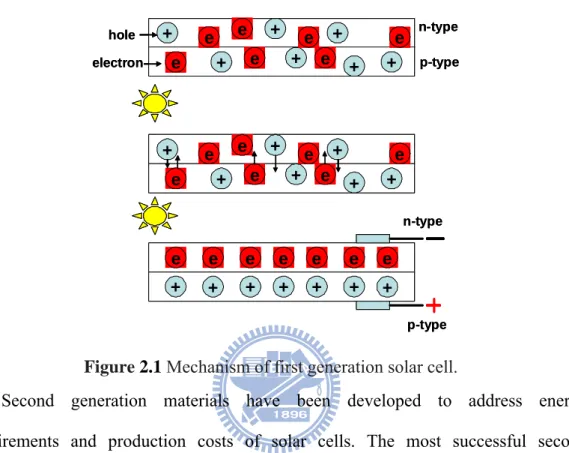
Crystalline silicon was first used to produce solar cells, and still dominates the PV market today. First generation is manufactured by silicon materials, the operation principle is shown as Figure 2.1, once sun light illuminate on the chip combined with two type semiconductors (p-n junction), electrons migrated to n-type semiconductor (holes migrated to p-type semiconductor) and consequently induced electricity. First generation cells consist of large-area, high quality and single junction devices. First Generation technologies involve high energy and labor inputs which prevent any significant progress in reducing production costs. Single junction
+ e e e e e + + + + e + + e hole electron + e e e e e + + + + e + + e n-type p-type + e e e e e + + + + + + e e n-type p-type + e e e e e + + + + e + + e hole electron + e e e e e + + + + e + + e n-type p-type + e e e e e + + + + + + e e n-type p-type
silicon devices are approaching the theoretical limiting efficiency of 31% [33] and achieve cost parity with fossil fuel energy generation after a payback period of 5–7 years.
Figure 2.1 Mechanism of first generation solar cell.
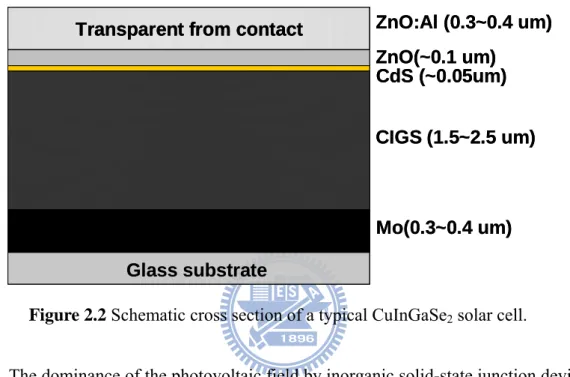
Second generation materials have been developed to address energy requirements and production costs of solar cells. The most successful second generation materials have been cadmium telluride (CdTe), copper indium gallium selenide (CIGS), amorphous silicon and micromorphous silicon. These materials are applied in a thin film to a supporting substrate such as glass or ceramics, reducing material mass and therefore costs. The thickness range of such a layer is wide and varies from a few nanometers to tens of micrometers. These technologies do hold promise of higher conversion efficiencies, particularly CIGS-CIS and CdTe offers significantly cheaper production costs. Typical CIGS materials are CuInSe2, CuInS2, CuInGaSe2 and their alloys with bandgaps ranging from 1.05 to 1.7 eV, which is favorable for absorbing the solar radiation. The high absorption coefficient of these materials of almost 105 cm-1 assures a complete absorption of the incident photon flux in an absorber layer as thin as a few microns. Polycrystalline chalcopyrite-based thin
Transparent from contact ZnO:Al (0.3~0.4 um) ZnO(~0.1 um) CdS (~0.05um) CIGS (1.5~2.5 um) Mo(0.3~0.4 um) Glass substrate
Transparent from contact
Transparent from contact ZnO:Al (0.3~0.4 um)
ZnO(~0.1 um) CdS (~0.05um)
CIGS (1.5~2.5 um)
Mo(0.3~0.4 um) Glass substrate
film solar cells have recently reached conversion efficiencies as high as 18.8%, [34] which is the highest value so far achieved for any polycrystalline thin film solar cell. This record device consists basically of a coevaporation-deposited p-type Cu(InGa)Se2 absorber layer, an n-type thin CdS buffer, and an n-type ZnO window layer, as shown in Figure 2.2.
Figure 2.2 Schematic cross section of a typical CuInGaSe2 solar cell.
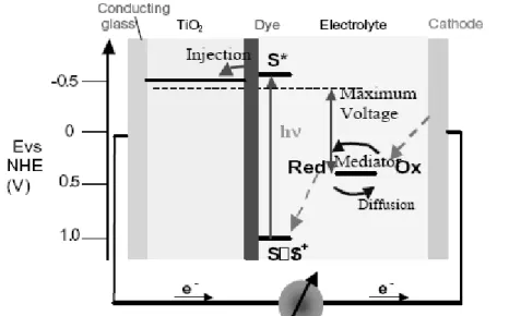
The dominance of the photovoltaic field by inorganic solid-state junction devices is now being challenged by the emergence of a third generation of cells, based, for example, on nanocrystalline and conducting polymers films. These offer the prospective of very low cost fabrication and present attractive features that facilitate market entry. It is now possible to depart completely from the classical solid-state junction device, by replacing the contacting phase to the semiconductor by an electrolyte, liquid, gel or solid, thereby forming a photo-electrochemical cell. The prototype of these devices is the dye-sensitized solar cell, which realizes the optical absorption and the charge separation processes by the association of a sensitizer as light-absorbing material with a wide band gap semiconductor of nanocrystalline morphology.
Third generation photovoltaic cell, also called advanced thin-film photovoltaic cell, is a range of novel alternatives to "first generation" (silicon p-n junction or wafer solar cells) and "second generation" (low-cost, but low-efficiency thin-film) cells. It is an even more advanced version of the thin-film cell. The dye-sensitized solar cell (DSSC) provides a technically and economically credible alternative concept to present day p–n junction photovoltaic devices [35]. In contrast to the conventional systems where the semiconductor assume both the task of light absorption and charge carrier transport the two functions are separated here. Light is absorbed by a sensitizer, which is anchored to the surface of a wide band semiconductor. Charge separation takes place at the interface via photo-induced electron injection from the dye into the conduction band of the solid. Carriers are transported in the conduction band of the semiconductor to the charge collector. A schematic presentation of the operating principles of the DSSC is given in Figure 2.3. At the heart of the system is a mesoporous oxide layer composed of nanometer-sized particles which have been sintered together to allow for electronic conduction to take place. The material of choice has been TiO2 (anatase) although alternative wide band gap oxides such as ZnO [36] has also been investigated. Attached to the
surface of the nanocrystalline film is a monolayer of the charge transfer dye. Photo-excitation of the sensitizer (S) is followed by electron injection into the conduction band of the mesoporous oxide semiconductor. The dye molecule is regenerated by the redox system, which itself is regenerated at the counter electrode by electrons passed through the load. Potentials are referred to the normal hydrogen electrode (NHE). The open-circuit voltage of the solar cell corresponds to the difference between the redox potential of the mediator and the Fermi level of the nanocrystallline film indicated with a dashed line.
p-type n-type Quantum dots p-type n-type Quantum dots
The other important new concept of third generation solar cell is quantum dots-based solar cell (Figure 2.4). Quantum dot (QD) solar cells have the potential
Figure 2.3 Principle of operation and energy level scheme of the dye-sensitized
nanocrystalline solar cell. [35]
to increase the maximum attainable thermodynamic conversion efficiency of solar photon conversion up to about 66% by utilizing hot photogenerated carriers to produce higher photovoltages or higher photocurrents. The former effect is based on miniband transport and collection of hot carriers in QD array photoelectrodes before they relax to the band edges through phonon emission (Figure 2.5). The latter effect is based on utilizing hot carriers in QD solar cells to generate and collect additional electron–hole pairs through enhanced impact ionization processes (Figure 2.6).
Current researches have introduced QDs into DSSC system to substitute for dye as the light absorber. [37, 38] They used ZnO nanowires and TiO2 nanotubes as the electrodes, combined with CdSe QDs as light absorber (see Figure 2.7 and 2.8). However, both the efficiency was less then 1 %, much lower than predicted value.
Figure 2.5 Idealized energy band diagram of a quantum dot solar cell. [8]
Figure 2.6 Enhance photovoltaic efficiency in quantum dot solar cell by impact
ionization. [9]
In spite of such low efficiency, QD-based solar cell is still worth to be developed. To overcome the bottleneck for higher efficiency, new QDs are necessary to be found and studied for their potential. CuInS2 is the most important candidate for this purpose.
In the next section, basic properties and synthesis methods of CuInS2 will be
introduced.
Figure 2.7 Schematic device of CdSe QD/ZnO-based DSSC. [37]
2.2 Brief Review of CuInS
2CuInS2 (CIS) is one of the ternary chalcopyrite compound family. A comprehensive review of chalcopyrite compounds was first reported by Shay and Wernick. [39] Recent experimental studies have been worked on thin film due to their great potential for large area PV modules. The structure and physical properties of CIS are further reported as follows.
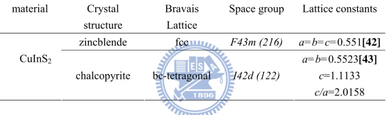
2.2.1 Crystal Structure of CuInS
2CIS has the chalcopyrite lattice structure. This is a diamond-like structure similar to the sphalerite (zincblende) structure but with an ordered substitution of the group I (Cu) and group III (In) elements on the group II (Zn) sites of sphalerite. This gives a tetragonal unit cell depicted in Figure 2.9 with a ratio of the tetragonal lattice parameters c/a close to 2 (see Table 2.1). The deviation from c/a = 2 is called the tetragonal distortion and stems from different strengths of the Cu–S and the In–S bonds. Structural and optical properties of chalcopyrite materials are compared in table 2.1. The reduced symmetry, due to two kinds of cations, leads to a primitive cell of eight atoms in the chalcopyrite structure compared to a primitive cell of two atoms in the sphalerite structure. The Bravais lattice of the chalcopyrite is body centered tetragonal, belonging to space group I42d. [40] Compared to the face centered cubic Bravais cell of the sphalerite the unit cell is doubled along the crystal c axis. At room temperature, the ternary compounds stabilize in chalcopyrite structure, however, they may crystallize in sphalerite structure at high temperature (975-1047°C) where the different cations are distributed randomly. [41]
(a) (b)
(a) (b)
Figure 2.9 Structures of (a) zincblende ZnS and (b) chalcopyrite CuInS2.
Table 2.1 Summary of crystal structure, space group, Bravais lattice, and lattice
constants of CuInS2 in the zincblende, chalcopyrite. material Crystal
structure
Bravais Lattice
Space group Lattice constants
zincblende fcc F43m (216) a=b=c=0.551[42] CuInS2
chalcopyrite bc-tetragonal I42d (122)
a=b=0.5523[43] c=1.1133 c/a=2.0158
2.2.2 Physical Properties
Figure 2.10 presents a schematic band structure of CIS, with notation of the contributions of the atomic orbitals. The valence band is separated into two parts, with the upper part reaching 5 eV and the lower one located around 7 eV. The Cu 3d and S 3p orbitals from the Cu-S bond contribute to the upper valence band whereas the S 3p and In 4p from the In-S bond form the lower valence band. At around 12 eV a band is built from S 3s states and a narrow band is set up near 17 eV by In 4d orbitals. The conduction band is formed by S 3p and In 5s orbitals. [44] This theoretical calculation of the band structure of CIS is in good agreement with the experimental results of X-ray photoemission spectroscopy in respect of the valence band structure. [45, 46] However, it underestimates the optical band gap relative to the experiment.
Figure 2.10 Schematic band structure of CuInS2, with indication of contributions of the atomic orbitals and the corresponding energy levels. Shade areas
denote the major subbands, and the boxed numbers mark the three internal gaps. [44]
CISis a direct semiconductor. Whereas bandgaps of 1.55 and 1.53 eV were found for bulk single crystals at low (2 K) and room temperature, respectively, band gaps varying between 1.38 and 1.55 eV were reported for CIS thin films at RT depending on different deposition techniques used. [39, 47-52] As is normally expected for semiconductors, the bandgap of CISfilms decreases with increasing temperature and can be characterized over the temperature range 300-77 K according to the relation
Eg = Eg0-βT2/(T+α) (2.1) with the initial bandgap Eg0=1.62 eV, two constants α =231.54 K and β = 4.3× 10⁻⁴eV/K, respectively. [52] Around the fundamental absorption edge, CIShas an absorption coefficient between 104to 105cm-1, it can thus absorb the incident light with photon energies higher than the bandgap within a few microns.
thin films have been reported. [53-58] Unlike its binary II-VI analogues that are normally n-type, CIScan be made both n- and p-type, depending upon its composition, i.e., deviation from molecularity and stoichiometry, defined as [Cu]/[In]-1 and 2[S]/([Cu]/3[In])-1, respectively. [59] It was generally observed that for CuInS2 single crystals good p-type behavior (ρ ~1-5 Ωcm, μ ~ 15-20 cm2/Vs) could be obtained by annealing in a sulfur overpressure, and good n-type characteristics (ρ ~1 Ωcm, μ ~ 100- 200 cm2/Vs), by annealing in indium or Cu + In with a minimum S pressure. [53, 54] Similar behavior was observed for CISfilms. Excess-sulfur films were generally p-type while sulfur-deficient and indium-rich films were n-type. [58] The observed behavior of the conducting type of CIScan be understood based on the predicted defect energies and on the ternary Cu-In-S phase diagram. In table 2.2, the defect levels of donors and acceptors reported for CuInS2 are summarized.
Table 2.2 Summary of the defect levels of donors and acceptors reported for
CuInS2.
Defect nature Defect assignment Ionization energy (eV) Refs
Acceptor VCu 0.10 [60-63]
Acceptor VIn 0.15 [64-66]
Donor VS(or InCu) 0.035 [61, 64-67]
Donor Ini (or InCu) 0.072 [64, 65]
2.3 Synthesis Methods of Nanocrystal CuInS
22.3.1 Solvothermal
In recent years, multinary chalcopyrite compounds have attracted much attention due to their interesting physical properties. It is well known that the device properties of CIS-based solar cells are badly affected by their stoichiometric composition, defects, and structure, which are strongly related to the preparation conditions. Some studies have been interested in the use of solvothermal routes, which are carried out at low temperatures and do not require organometallic or toxic precursors, to prepare various kinds of nanocrystalline materials with a wide range of optical and electronic properties accessible in nanoscale.
Jiang et al. [68] synthesized CIS nanorod at 280oC through elemental solvothermal reaction. Starting materials were analytical grade Cu, In, and S powders. Ethylenediamine was used as solvent. The XRD pattern of this retragonal phase yielded cell constants a = 5.5086 A, c = 11.0264 A, close to the reported data (JCPDS card, no.38-777). The TEM image (Figure 2.11) indicated that CIS is a nanorod with size of 20 nm x 800 nm.
Figure 2.11 TEM image of CIS nanorod. [39]
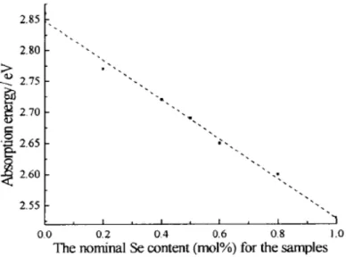
semiconductor CuIn(SexS1-x)2 nanocrystallities with composition x ranging from 0 to 1 using CuCl2.2H2O, InCl3.4H2O, Se and S as reactants. In their system, ethylenediamine was selected as the solvent due to its strong basic capacity, strong chelation, and its ability to act as an absorber of the excess heat produced in the reaction. UV-Vis absorption spectra indicate that the absorption energy varies linearly with the Se/S ratio (as shown in Figure 2.12).
Figure 2.12 The dependence of absorption energy on the norminal Se content (mol
%) for the samples. [69]
2.3.2 Single-source precursor
Colloidal synthesis of nanoparticles provides better control over morphology and size than other methods, particularly for very small particles. Single-source precursors are attracted great intention due to controllable and specific properties. Single-source precursors are discrete molecules that include all the elements required in the final materials these precursors can be designed with many properties in mind, including stoichiometry, solubility, and volatility.
Castro et al. synthesized CIS and CISe nanocrystals through single-source precursors in 2003, [70] using (PPh3)2CuIn(SEt)4 and (PPh3)2CuIn(SePh)4 (scheme
and molecular structure are shown in scheme 2.1 and Figure 2.13). Although the particle size of CIS they synthesized is not small enough (larger than 8.1 nm) to exhibit size quantization effects, these precursors provide a route to colloidal chalcopyrite QDs.
Figure 2.13 Molecular structure of (PPh3)2CuIn(SEt)4. [70]
Scheme 2.1 Reaction scheme for the conversion of the single-source precursors to
CuInS2 and CuInSe2
It is well-established that quantum confinement in semiconductors (i.e. increasing bandgap energy with decreasing semiconductor dimension) takes place at particle dimensions smaller than the Wannier-Mott (WM) exciton of the corresponding macroscopic bulk phase. [71] by knowledge of the high frequency dielectric constant, ε∞, and the reduced effective exciton mass, μ = 1/(μe-1 + μh-1 ), one can calculate the WM-exciton Bohr radius according to RB = (ε∞/μ) aB, with aB being the Bohr radius of the hydrogen atom (0.53 A). Taking the CIS bulk values [72] of ε∞ = 11, μe = 0.16 and μh = 1.3, the WM-exciton size of CIS was calculated to
be 8.1 nm.
In 2004, they successfully synthesized CIS nanocrystals smaller than 8.1 nm by modifying experiment condition. [73] The average size of these CIS nanocrystals varied from 2 nm, 2.68, and 3.35 nm with increasing temperature 200oC, 225oC, and 250oC (Figure 2.14). The absorption of these nanocrystal solutions show a broad shoulder with a long tail to lower energies, both significantly shifted from the bulk band-gap absorption of CIS (1.5 eV), resulting from quantum confinement. Shown in Figure 2.15(a) are typical absorption, emission, and photoluminescent excitation spectra for solutions of CIS colloidal nanocrystals.
Figure 2.14 TEM images of CuInS2 nanocrystals grown at 225 and 250oC. Scale bars in the images are both 5 nm. [73]
Based on their study, the nature of the surface ligands plays an important role in the PL efficiency of CIS nanocrystals. As has been observed for CdSe nanocrystals, surface defects provide sites for charge trapping, leading to nonradiative recombination of the electron and hole and quenching of the fluorescence emission. Passivation of these sites with a strong ligand leads to increased quantum yield, while a weak ligand further increases the quenching effect. As can be seen in Figure 2.15(b),
the PL efficiency is strongly affected by the nature of the surface ligands, which implies that the surface ligands of the nanocrystals provides a significant source of defects or unpassivated sites where nonradiative recombination can take place.
Figure 2.15 (a) Absorption, fluorescence emission, and photoluminescent excitation
spectra of a typical colloidal solution of CIS nanocrystals. (b) Absorption and fluorescence emission spectra of CIS with hexanethiol, TOPO, and pyridine organic capping ligands (from top to bottom). [73] Nairn et al. have also found the similar effect (Figure 2.16) in 2006, [74] which synthesized CIS nanocrystals through single-source precursor photolysis. They prepared the molecular precursors [(TOP)2CuIn(SR)4] (TOP = (octyl)3P; R = n-Pr, t-Bu) in organic solvent such as DOP, and then irradiated the precursors with a medium pressure Hg arc lamp (200 W/in.). The gradual color transition of the solution changed from colorless to yellow to orange and ultimately orange-red, as shown in Figure 2.17. The PL properties of CIS nanocrystal are complex due to its complicated defect chemistry from variation in molecularity ([Cu]/In) and stoichiometry ([S]/[Cu]). Examples of defects are copper and indium vacancies and interstitials, and excess or deficient sulfur occupancy. CIS can be prepared as either n- or p-type conductivity by varying the atomic ratios. High-quality crystalline material
Figure 2.16 Effect of different capping agents on the emission intensities of CIS
nanocrystals generated from the photolysis. [74]
of both conductivity types displays narrow band-edge emission between 1.5 and 1.55 eV, consisting of up to 10 narrow lines. These transitions arrive from recombination of free excitons, excitons bound to neutral or ionized donors and acceptors, and donor-valence band pairs; Figure 2.18 shows these energy levels and transitions. Based on the large difference between the absorption and the emission peaks and the observation of the PL at room temperature, it is concluded that PL of these CIS nanocrystals is broad-band, or donor-acceptor defect based, in nature. It is not surprising that CIS synthesized at a very low temperature would have many defects. It is difficult to grow CIS that exhibits near-edge PL, and that materials is synthesized at 700-900oC
Figure 2.17 Vials of samples from the irradiation of solution of precursor
[(TOP)2CuIn(SR)4] in DOP for (from left to right) 0, 2, 4, 6, 8, 11, 21, 30, 50, 74, 214, and 218 h. [74]
Figure 2.18 Schematic diagram of the energy levels and transitions that have been
observed in single-crystal CIS. [73]
2.3.3 Hot-Injection
Development of colloidal routes enable low-cost fabrication of inorganic solar cells through a wet-chemistry process of semiconductor nanocrystal colloidal solution has attracted a great deal of attention. It has been known that crystal structure, composition, and size of the nanocrystals may significantly affect their optoelectronic property and device performance. Although the structure of nanocrystals can be generally controlled by the capping ligands used, the reported Cu-In-S nanocrystals are still limited to the chalcopyrite structure. Nevertheless, composition of current Cu-In-S nanocrystals is mainly controlled by using a single ternary precursor. In spite of the use of a single-source precursor is convenient, this method is limited by the precursor availability and their tedious procedure.
In 2006, Nakumura et al. introduced Zn into CIS system with a kind of hot-injection method and enhanced their PL intensity. [75] The particle size varied from 2.6 to 4 nm with increasing Cu/Zn ratio, both the absorption and emission peaks also show red-shifted with increasing Cu/Zn ratio (Figure 2.19).
Figure 2.19 Raw material composition effects on optical properties: (a) UV-vis
absorption and (b) PL emission spectra (excitation 500 nm). (Raw material composition Zn:Cu;In:S = 1:n:n:4 (n = 0.5-5).) [75]
In a chalcopyrite CIS, the Cu-S bond is weaker than that of In-S and the Cu vacancy is preferably generated. In addition, the Cu vancancies induced anti-site defect generation [76] and the ionic diameters of Cu and Zn are similar. On the basis of reasons above, Zn preferentially substituted to Cu and prevented anti-site defects. Therefore, introduction of Zn ion into CIS nanocrystals was predicted to improve the PL intensity. Furthermore, the band-gap was controlled by this Zn content. The wide selectivity in components and composition by this method suggest a new series of chalcopyrite-type semiconductor nanocrystals with various properties.
Different crystal structures were obtained through a hot-injection method on Cu(dedc)2 and In(dedc)3 precursors (dedc is diethyldithiocarbamate.), with tunable [Cu]/[In] composition. [77] Zincblende CIS nanocrystals can be obtained by the co-decomposition of Cu(dedc)2 and In(dedc)3 in the presence of oleic acid. Similarly, wurtzite CIS nanocrystals can be prepared by the co-decomposition of Cu(dedc)2 and In(dedc)3 in the presence of dodecanethiol. The formation of CIS nanoparticles may
involve possible reaction routes illustrated in Scheme 2.2: the reaction of CuS or Cu2S from the decomposition of the Cu(dedc)2 in the presence of oleic acid or dodecanethiol with In2S3 from In(dedc)3, respectively, results in the formation of zincblende and wurtzite CIS nanocrystals.
Scheme 2.2 Schematic formation mechanism of CIS from Cu(dedc)2 and In(dedc)3 precursors. [77]
This study correlates the crystalline structure of the binary ZnS nanocrystals with those of ternary Cu-In-S nanocrystals, demonstrating the feasibility fabrication their alloyed or core/shell structures.
Chapter 3
Experiment
3.1 Chemicals
Copper(I) chloride (CuCl, 95%, analytical reagent), indium(III) chloride (InCl3, 98%, AR), sulfur powder (99.5%, chemically pure), Zinc stearate (10~12% as Zn, technical) and trioctylphosphine (TOP, 90%, technical grade) were purchased from Sigma-Aldrich Corp.; octadecene (ODE, 90%, technical grade) and oleylamine (70%, technical grade) were purchased from Tokyo chemical industry Co., Ltd. Diethyldithiocarbamic acid zinc salt ([(C2H5)2NCSS]2Zn, technical grade), zinc nitrate hexahydrate (Zn(NO3)2.6H2O), methenamine (C6H12N4), mercaptopropionic acid (MPA) were purchased from Sigma-Aldrich Corp.
3.2 Characterization
3.2.1 Structure and morphology X-ray diffraction (XRD)
The resulting powdercollected from the solutions was examined using X-ray powder diffraction (XRD, M18XHF, Mac Science, Japan) to identify the crystallographic phase of nanocrystals, with Cu Kα radiation (λ=0.15405 nm) (40kV, 200 mA), 2θ ranging from 10o to 70o at a scanning rate of 10o /min.
Transmission electron microscope (TEM)
TEM images were obtained using a JEOL 2010 transmission electron microscope operating at 200 kV. Samples for the TEM were prepared by depositing a drop of the samples dispersed in toluene onto a carbon grid. The excess liquid was wicked away with filter paper, and the grid was dried in air.
X-ray photoelectron spectroscopy (XPS)
XPS measurements were carried out using a Field Emission – Auger Electron Microprobe (Thermo VG Microlab 350) x-ray photoelectron spectrometer using an Mg Kα x-ray as the excitation source.
3.2.2 Optical measurement
Then UV-vis, PL emission, and excitation (PLE) spectroscopy was applied using a UV-vis spectrophotometer (UV-1600; Agelent 8453) and a spectrofluorometer (FP-6600; Jasco, Inc., Japan). For these observations, the products were precipitated with alcohol. They were further isolated by centrifugation to remove excess surfactants. The centrifuged particles were redispersed into an organic solvent such as toluene to yield a clear and colloidally stable suspension. The amounts of Zn-CIS absorbed on the ZnO films were measured with an UV-visible-NIR spectrophotometer (JASCO V-570) equipped with an integrating sphere (JASCO ISN-470).
3.3.3 Solar parameter measurement
Measurements of IV curves were made with a digital source meter (Keithley 2400, computer-controlled) with the device under one-solar AM 1.5 irradiation of a solar simulator (Newport-Oriel 91160) calibrated with a Si-based reference cell (Hamamatsu S1133) and a IR-cut filter (KG5) to correct the spectral mismatch of the lamp. The Zn-CIS/ZnO devices were operated in a back-side illumination fashion with the transparent counter electrode masked by a black plastic tape of the same size with a round hole to allow the actively illuminated area of 0.28 cm2 for all measurements. Time-resolved measurements were performed with a tunable nanosecond optical-parametric-oscillator/Q-switch-pumped neodymium doped
yttrium aluminum garnet laser system NT341/1/UV, Ekspla. Emission transients were collected with a monochromator SpectraPro-300i, ARC, detected with a photomultiplier tube R928HA, Hamamatsu connected to a digital oscilloscope LT372, LeCroy, and transferred to a computer for kinetic analysis.
3.2.4 High frequency magnetic field set up
A high frequency (50-100 kHz) magnetic field (HFMF) was applied to the precursors to provide kinetic energy for Zn-CIS nanocrystal synthesis. The HFMF was created by a power supply, function generator, amplifier, and cooling water. Similar equipment was also reported in PNAS, vol. 103, 3540–3545 (2006). The strength of the magnetic field depended on the coils. In this study, the coil was 8 loops, the frequency was 50 kHz and the strength of magnetic field (H) was 2.5 kA/m. The temperature of HFMF generator was controlled by cycling cooling water at 25 oC.
Hysteresis loop analysis
Measurements of magnetization (M) versus applied field H and temperature T were carried out using a commercial SQUID (superconducting quantum interference device) magnetometer (MPMX-XL7).
3.3 Material fabrication
3.3.1 Synthesis of CuInS2 nanocrystals
The CIS nanocrystals were prepared using a high-temperature organic solvent process. First, sulfur was dissolved in TOP. The solution was diluted with ODE to form a clear solution (solution 1). Then, CuCl and InCl3 were dissolved in oleylamine at 50oC to form another solution (solution 2). These two material solutions were mixed to produce a raw material solution. A small aliquot of raw material solution was put into
a test tube and soaked directly in an oil bath that had been preheated to 240oC and aged for 300s. The prepared solutions were limpid, reflecting their high colloidal stability.
3.3.2 Synthesis of CuInS2@ZnS core/shell nanocrystals
Preparation of the CIS@ZnS core/shell nanocrystals was achieved by modifying the above reaction system and surface coating of ZnS. Zinc stearate (ZnSt) and sulfur were each dissolved in TOP (solutions 3 and 4). After the colloidal solution of CIS nanocrystals was preheated to 240oC, solutions 3 and 4 were injected into the solution for 300s. Subsequently, the mixture was cooled to 90oC to form the ZnS shell on the surface of CIS nanocrystals. Repeating the injection step were also used to grow the multiple ZnS layers on the CIS nanocrystals. The product was diluted with toluene and PL spectra were measured.
3.3.3 Systhesis of ZnO nanowire
The ZnO thin films were deposited on F-doped SnO2 (FTO, 30 Ω/sq, Sinonar, Taiwan) substrates by RF magnetron sputtering as followed from our previous report.[126]
The seeded substrates were then suspended horizontally in a reagent solution containing 0.016 M zinc nitrate and 0.025 M methenamine and heated to 95°C to initiate nanowire growth.
3.3.4 Synthesis of Zn-CIS quantum dots
The Zn-CIS QDs were prepared using a high-temperature organic solvent process. 0.5 mmol diethyldithiocarbamic acid zinc salt was dissolved in 6 ml TOP. The solution was diluted with 24 ml ODE to form a clear solution (solution 1). Then, 0.2 mmol CuCl and InCl3 were dissolved in 6 ml oleylamine at 50oC to form another solution
(solution 2). Here, amine coordinates the Cu and In ions to produce amine complexes. These two material solutions were mixed to produce a raw material solution with a ratio Zn:Cu:In:S = 1:n:n:4 (n=1 in this composition), the composition ratios of Cu and In were varied from 1 to 3. Those of Zn and S precursors were fixed in concentration, indicated as Zn:Cu:In:S = 1:n:n:4 (n=1-3). A small aliquot of raw material solution was put into a test tube and soaked directly in an oil bath that had been preheated to 240oC and aged for 300s. The prepared solutions were limpid, reflecting their high colloidal stability.
3.3.5 ZnS coating of Zn-CIS quantum dots
A colloidal solution of ca. 20 mg of Zn-CIS nanocrystals with an average diameter of 3.6 nm in 4 mL of toluene was placed in a three-neck flask under purified argon flow. After addition of 2.5 mL of TOPO, the mixture was heated to 190 °C and then kept at this temperature till a complete heptane evaporation. Zinc stearate (316 mg) was dissolved in 2.5 mL of toluene upon gentle heating (ca. 60 °C). After cooling to room temperature, the resulting 0.2 M solution was mixed with 2.5 mL of a 0.2 M solution of Se in TOP. By means of a syringe pump this mixture was injected within 1 h into the reaction flask containing the core nanocrystals at 190-200 °C. Periodically small aliquots were removed in order to monitor the shell growth. After the addition was completed the crystals are annealed at 190 °C for an additional 1-1.5 h.
3.3.6 Synthesis of hydrophilic quantum dots by ligand exchange
Purified QDs were dissolved in a minimum amount of chloroform and excess mercaptopropionic acid (MPA) was added until the solution became cloudy, and stirred at 55°C for one night in argon atmosphere. After that, 1mL of tetrahydrofuran (THF) was added to stop the surface exchange reaction. After cooling to room
temperature, a suspension of potassium t-butoxide in THF was added to neutralize the carboxyl acid function, and then centrifuged to remove the by-products with THF. The THF washing process was repeated for 2-3 times, and finally distilled water was added to disperse hydrohilized Zn-CIS NCs into water.
3.3.7 Assembling Zn-CIS quantum dots on ZnO Nanowires
Fire ZnO plate at 450oC for 30 minutes and then after cooling in air for 5 minutes, transferred ZnO plate to ZCIS solution and left for 3 days to ensure saturated adsorption of Zn-CIS QD onto the ZnO nanowires.
3.3.8 Fabrication of solar cells
For characterization of the photovoltaic performance of our devices, the Zn-CIS/ZnO films were served as working electrode (anode); a fluorine doped tin oxide glass (typical size 1.0×2.0 cm2) coated with platinum (Pt) particles by sputtering was used as a counter electrode (cathode). The two electrodes were assembled into a cell of sandwich type and sealed with a hot-melt film (SX1170, Solaronix, thickness 25 μm); a thin layer of electrolyte was introduced into the space between the two electrodes and the device was fabricated accordingly. A typical redox electrolyte contained 0.1 M lithium iodide (LiI), 0.01 M iodine (I2), 0.5 M 4-tert-butylpyridine (TBP), 0.6 M butyl methyl imidazolium iodide (BMII), and 0.1 M guanidinium thiocynate (GuNCS) in a mixture of acetonitrile (CH3CN, 99.9%) and valeronitrile (n-C4H9CN, 99.9%) (v/v = 15/1)
3.3.9 Synthesis of Zn-CIS nanocrystals in the presence of high frequency magnetic field
solution was diluted with 24 ml ODE to form a clear solution (solution 1). Then, 0.2 mmol CuCl and InCl3 were dissolved in 6 ml oleylamine at 50oC to form another solution (solution 2). Here, amine coordinates the Cu and In ions to produce amine complexes. These two solutions were mixed to produce the raw material solution. A small aliquot of raw material solution was put into a test tube and exposed to HFMF with an input power of 90 W (Figure 6.1). The color of the mixture solution was changed with different durations of HFMF exposure from yellow (30 sec), red (45 sec) to black (120 sec). The resulting precipitated powders were collected via centrifugation at 6000 rpm, removed from the solution, and repeated three times to remove excess surfactants which were precipitated using methanol.
3.3.10 Fabrication of Zn-CIS thin film solar cells
The Mo coated soda lime glass substrates used here was fabricated by dc magnetron sputtering at Ar pressures 1.5 mTorr resulting in a 200 nm layer. Deposition of the CIS absorber layer on top of the Mo substrates is used drop casting by the nanoink solution and subsequent thermal treatments to remove the organics and sinter the films under Ar and Se atmospheres at 500 oC respectively. A ~ 50 nm CdS layer is then deposited by a chemical bath deposition (CBD) technique. The CBD bath contains 183 ml of deionized H2O, 25 ml of 0.015 M CdSO4 solution, 12.5 of 1.5 M thiourea solution, and 31.25 ml of stock NH4OH (Aldrich). Next, A ~50 nm high resistivity i-ZnO film capped with a ~300 nm high conductivity ITO layer are deposited by RF magnetron sputtering. The ZnO film is sputtered in a mixture of 10% O2 in Ar at sputtering pressure of 10 mTorr with no intentional heating. The ITO layer is sputtered with neither O2 nor intentional heating at sputtering pressure of 1 mTorr. After sputtering of the oxide layers, the final device is baked in air at 200 oC over night.
Chapter 4
Synthesis and Characterization of Highly Luminescent CuInS
2and
CuInS
2/ZnS (Core/Shell) Nanocrystals
4.1 Introduction
CuInS2 is one of the most important I-III-VI2 semiconductor materials for use in photovoltaic solar cells and it has many notable advantages such as an appropriate band gap, a high absorption coefficient, and good thermal, environmental, and electrical stability. [78-80] Also, some research aims to apply chalcopyrite materials in “spintronics” as tailorable ferromagnetic materials. [81-84] However, chalcopyrite NCs have not been systematically investigated and relatively few studies [70, 73, 75,
85-86] have achieved particle sizes small enough to exhibit quantum confinement (the
Wannier-Mott bulk exciton of the CuInS2 is 8.1 nm [86]). Although Nairn et al. combined single source precursors and photolysis methods to obtain CuInS2 NCs ~2 nm in diameter, the photoluminescence (PL) in these chalcopyrite NCs were not so strong as the well-developed II-VI group semiconductor NCs (CdSe, CdS et al.). [85] Nakamura and coworkers modified the high-temperature organic solvent method and successfully introduced Zn into the CuInS2 NCs to achieve tunable band-gap energies (Eg) and PL. Compared to the pure CIS NCs prepared by a similar method, it was found that the quantum yield for the Zn-CIS alloy (~5%) was still much less than that of CdSe. [76]
Expansion of typical II-VI group semiconductor NCs such as CdSe and PbS are necessary because of the “Restriction of the Use of Certain Hazardous Substance (RoHS)” in Europe. Based on considerations of environmental and human toxicity, biological studies confine these NCs to specific fields. Luminescent CIS NCs are sought as new candidates for building blocks of nanomaterials and biological tabs
![Figure 2.5 Idealized energy band diagram of a quantum dot solar cell. [8]](https://thumb-ap.123doks.com/thumbv2/9libinfo/8763050.208647/25.892.197.705.289.974/figure-idealized-energy-band-diagram-quantum-solar-cell.webp)
![Figure 2.7 Schematic device of CdSe QD/ZnO-based DSSC. [37]](https://thumb-ap.123doks.com/thumbv2/9libinfo/8763050.208647/26.892.193.690.190.1004/figure-schematic-device-cdse-qd-zno-based-dssc.webp)
![Figure 2.13 Molecular structure of (PPh 3 ) 2 CuIn(SEt) 4. [70]](https://thumb-ap.123doks.com/thumbv2/9libinfo/8763050.208647/33.892.188.697.288.777/figure-molecular-structure-pph-cuin-set.webp)

![Figure 2.17 Vials of samples from the irradiation of solution of precursor [(TOP) 2 CuIn(SR) 4 ] in DOP for (from left to right) 0, 2, 4, 6, 8, 11, 21, 30, 50, 74, 214, and 218 h](https://thumb-ap.123doks.com/thumbv2/9libinfo/8763050.208647/36.892.134.765.809.1032/figure-vials-samples-irradiation-solution-precursor-cuin-right.webp)
