SrTiO
3
–SiO
2
oxide films for possible high-k gate dielectric applications
Chun-Chieh Lin, Li-Wen Lai, Chih-Yang Lin, Tseung-Yuen Tseng
⁎
Department of Electronics Engineering and Institute of Electronics, National Chiao Tung University, Hsinchu 300, Taiwan Available online 6 May 2006
Abstract
Amorphous thin films of SrTiO3–SiO2high-k dielectric oxides were deposited on p-Si substrate by sputtering from the targets made by SrTiO3
and SiO2powder mixtures. The surface morphology, crystal structure, chemical bonding configuration, and depth profile of the composition were
investigated by using scanning electron microscopy, glancing incident angle X-ray diffraction, X-ray photoelectron spectroscopy, and Auger
electron spectroscopy, respectively. The capacitance–voltage (CV) and current–voltage characteristics were used for demonstrating their electrical
properties. The SrTiO3–SiO2thin films remained as amorphous structures when annealed up to 900 °C. The Pt/SrTiO3–SiO2/Si MOS structure
had a low leakage current density of∼2×10− 8A/cm2measured at 100 kV/cm and dielectric constant of 24 for 700 °C-annealed film. The films
annealed at 600 °C showed typical CV characteristics. However, the deformed CV curves were found for films annealed at 700 °C due to the
diffusion of Ti species in the SrTiO3–SiO2film into the Si substrate.
© 2006 Elsevier B.V. All rights reserved.
Keywords: High-k; Gate oxide; Leakage current; Dielectric constant
1. Introduction
In order to follow the international technology roadmap for semiconductors, the thickness of SiO2gate oxide has to be less
than 2 nm in the near-term technology requirements [1]. However, when the gate oxide thickness has been reduced to less than 2 nm, the gate leakage current will approach the limit of 1 A/cm2 at an applied gate voltage of 3 V [2]. Such an increase of gate leakage current is due to the mechanism of direct tunneling, which leads to the undesired power consump-tion in CMOS devices[3].
Since high-k gate dielectrics can provide a thicker physical thickness to reduce the leakage current flowing through the gate oxide, various high-k gate dielectrics have been investigated to replace the conventional SiO2gate dielectric in the past several
years[2–5]. Among the various possible candidates of high-k gate dielectrics, SrTiO3(STO) plays a good role because of its
large dielectric constant [6,7]. However, the crystallization temperature of STO is too low to conform to the integration technology. On the basis of the previous reports [2,8], the crystallization temperature of the oxides, such as ZrO2 and
HfO2, can be increased due to the addition of SiO2. However,
there is no report on the STO–SiO2oxide system used as gate
dielectrics. The objective of this study is to produce an amorphous thin film which is expected to have a lower leakage current density compared to polycrystalline film. Therefore, SiO2 was added into STO to increase its crystallization
temperature. It was shown in this study that the STO–SiO2
oxide thin film retains its amorphous nature up to an annealing temperature of 900 °C. Furthermore, the microstructure and electrical properties of the STO–SiO2 oxide films were also
investigated.
2. Experimental details
The boron doped p-type 4-in. Si (100) wafers were cleaned by a standard RCA cleaning process [9] and then chemically etched by dipping in dilute HF solution to remove the native oxide from the Si substrates. After the cleaning processes, the STO–SiO2thin films were deposited at 300 °C on Si substrates
by radio-frequency (rf) magnetron sputter from a powdered target, which was made from a mixture of 50 mol% of STO and 50 mol% of SiO2 powders. The STO–SiO2 thin films were
prepared at a fixed power of 100 W, background pressure of 1.33 × 10− 4Pa (1 × 10− 6Torr), and working pressure of 1.33 Pa (10 mTorr), which was maintained by a mixture of Ar and N2at
a fixed ratio of 4:1 with a total flow of 10 sccm. To study the
Thin Solid Films 515 (2007) 8005–8008
www.elsevier.com/locate/tsf
⁎ Corresponding author. Tel.: +886 3 5731879; fax: +886 3 5724361. E-mail address:[email protected](T.-Y. Tseng).
0040-6090/$ - see front matter © 2006 Elsevier B.V. All rights reserved. doi:10.1016/j.tsf.2006.03.054
effect of SiO2addition on the crystallization temperature, on a
separate study, the pure STO film was also deposited on the Si substrate using the same sputtering process, but pure STO powdered target was used.
After the deposition, the films were heat-treated by using a rapid thermal annealing furnace in N2ambient at temperatures
ranging from 600 to 900 °C for 1 min. The surface morphology and the thickness of the films were characterized by scanning electron microscopy (SEM, Hitachi S4700) with the operating voltage of 5 kV. The crystal structure of the films was identified by glancing incident angle X-ray diffraction (GIAXRD, Rigaku D/ MAX2500) with Cu Kα radiation and an incident angle of 2°. The chemical bonding state of the films was investigated by using X-ray photoelectron spectroscopy (XPS, VG ESCA-210D) with Al Kα radiation (1486.6 eV). The X-ray radiated at an incident angle of 45° from the sample surface and the photoelectron emission was received by a concentric hemispherical analyzer at a take-off angle of 90°. No sputter-etching was performed on the sample prior to the XPS examination. The compositional depth profiles of the films were measured by using Auger electron spectroscopy (AES, VG Microlab 310F) with an electron beam accelerating voltage of 10 kV and a beam current of 0.4μA. The ion beam etching profile was accomplished with an Ar ion beam voltage of 3 kV and emission current of 100 mA.
For the electrical measurement, Pt top electrodes were deposited on the films by e-gun evaporation through a shadow mask of an area of 4.9 × 10− 4cm2and then annealed at 400 °C for 5 min. An Al back side substrate electrode was deposited by thermal evaporation. The capacitance–voltage (CV) measure-ments were performed using the Agilent 4284A at 50, 100, 500 kHz, and 1 MHz. The current–voltage characteristics were recorded using the Agilent 4156A.
3. Results and discussion
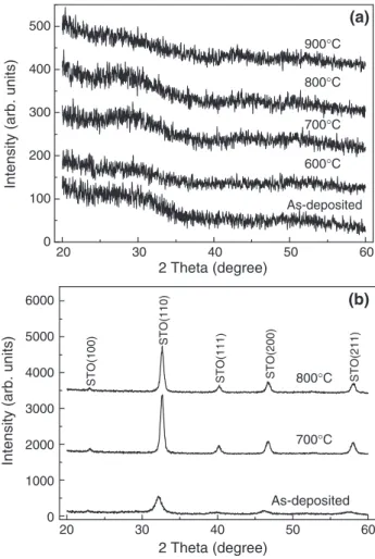
Fig. 1(a) shows the GIAXRD patterns of STO–SiO2oxide
films deposited at 300 °C and then annealed at 600, 700, 800, and 900 °C, indicating no diffraction peaks of the crystallized phases in these films. That is, these oxide films retain an amorphous nature when annealed up to 900 °C. These films have a low leakage current density of ∼2×10− 8 A/cm2 measured at 100 kV/cm, which can be attributed to the amorphous-type gate oxides with superfine grains that have large amount of high resistive grain boundaries. Nevertheless, pure STO oxide films deposited at 300 °C and then annealed at 700 and 800 °C are crystalline in structure as depicted by the GIAXRD patterns ofFig. 1(b). Consequently, the difference in the crystal structure between the STO–SiO2and the pure STO
films can be easily recognized.
Fig. 2shows the SEM image of the cross section of the STO–
SiO2thin film annealed at 700 °C indicating that the thickness of
the film is about 69 nm, which includes about 10 nm of the interface oxide layer. In addition, the surface morphology of the film was smooth, which is an important physical property that may affect the electrical properties of the film.
The dielectric constants of the as-deposited, 600, 700, and 800 °C-annealed STO–SiO2oxide films were 17.9, 23.7, 23.6,
and 19.5, respectively. The dielectric constant of the films is expected to be between the dielectric constant of SiO2(3.9) and
STO based on the mixture rule. In our experimental results, the dielectric constants of STO–SiO2films were located between
18 and 24. It can be anticipated that the dielectric constant decreases with an increase in the SiO2 content at the same
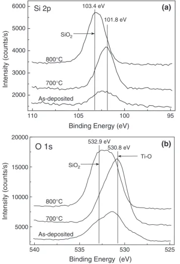
annealing temperature. The dielectric constant displays a slight lowering for the 800 °C-annealed film compared to those of the 600 and 700 °C-annealed films. These results can be explained by the XPS spectra of the STO–SiO2oxide films (Fig. 3). The
0 1000 2000 3000 4000 5000 6000 STO(100) STO(110)
STO(111) STO(200) STO(211)
(b)
As-deposited
Intensity (arb. units)
20 30 40 50 60 0 100 200 300 400 500 (a) 900°C 800°C 700°C 600°C 800°C 700°C As-deposited
Intensity (arb. units)
2 Theta (degree)
20 30 40 50 60
2 Theta (degree)
Fig. 1. GIAXRD patterns of: (a) STO–SiO2oxide films deposited at 300 °C and
then annealed at 600, 700, 800, and 900 °C and (b) pure STO oxide films also deposited at 300 °C and then annealed at 700 and 800 °C.
Fig. 2. SEM cross section image of the STO–SiO2 oxide film annealed at
700 °C.
high resolution XPS spectra of Si 2p core levels of the as-deposited, 700 and 800 °C-annealed films are shown inFig. 3
(a). The Si 2p photoelectron line of the Si–Si bond was reported to be situated at about 98.9 eV [10] and the SiO2 bonds at
103.4 eV [11]. Nevertheless, the binding energy of Si 2p corresponding to STO–SiO2 has not been reported in the
previous literatures. As indicated inFig. 3(a), the main peak of the Si 2p signal of the 700 °C-annealed film is at 101.8 eV, which is inferred to be the Sr–O or Ti–O bonds that can be supported by the XPS spectrum (Fig. 3(b)) shown in the next section. However, the main peak of the Si 2p photoelectron line of the 800 °C-annealed film is situated close to the SiO2bonds.
Consequently, the binding energy of STO–SiO2in the 700
°C-annealed film is much stronger than this in the 800 °C-°C-annealed film, while some amount of SiO2in the 800 °C-annealed film
appears to be possibly segregated from the film, which can explain why the 700 °C-annealed film has a higher dielectric constant.
Another XPS spectrum can support the above explanation.
Fig. 3(b) displays the XPS spectra of the O 1s signals of the as-deposited, 700 and 800 °C-annealed films. As revealed in this figure, the main peak of the O 1s signal of the 700 °C-annealed film is at 530.8 eV, which is the typical binding energy of the O
1s signal corresponding to Ti–O[12]. Nevertheless, the main peak of the 800 °C-annealed film is at 532.9 eV, which corresponds to the SiO2bonds[13]. Hence, the binding energy
of STO–SiO2in the 700 °C-annealed film is very strong and the
O 1s signal is less effective from the SiO2, which is consistent
with the result shown in Fig. 3(a). Again, it is supported that
110 105 100 95 2000 3000 4000 5000 6000 SiO2 SiO2 101.8 eV 103.4 eV As-deposited
Binding Energy (eV)
(a) 800°C 700°C As-deposited 800°C 700°C Si 2p Intensity (counts/s) 540 535 530 525 5000 10000 15000 20000 (b) Ti-O 530.8 eV 532.9 eV
Binding Energy (eV)
O 1s
Intensity (counts/s)
Fig. 3. XPS spectra of the as-deposited, 700 and 800 °C-annealed STO–SiO2
films: (a) high resolution selective spectrum of Si 2p and (b) high resolution selective spectrum of O 1s. 0 -6 -5 -4 -3 -2 -1 0 1 2 3 4 20 40 60 80 100 120 140 160 180 200 C (pF) VG (V) -6 -5 -4 -3 -2 -1 0 1 2 3 4 VG (V) 50 kHz 100 kHz 500 kHz 1 MHz 50 kHz 100 kHz 500 kHz 1 MHz (a) (b) 0 20 40 60 80 100 120 140 160 180 200 C (pF)
Fig. 4. CV curves of the STO–SiO2oxide films annealed at: (a) 700 and (b)
600 °C at four different frequencies indicated.
0 200 400 600 800 1000 1200 1400 0.0 0.5 1.0 1.5 2.0 2.5 Si O Ti Sr Intensity (counts/eV/s) Sputter-etching Time (s) Si Substrate Ti (x106)
Fig. 5. AES depth profile of the 700 °C-annealed STO–SiO2oxide film.
8007 C.-C. Lin et al. / Thin Solid Films 515 (2007) 8005–8008
some SiO2was possibly separated from the 800 °C-annealed
film, which results in its lower dielectric constant.
The CV characteristics of the STO–SiO2films were measured
from the inversion region to accumulation region (from positive to negative bias voltage).Fig. 4(a) depicts the CV curves of the 700 °C-annealed films measured at four different frequencies, indicating that the capacitance in the inversion region increases dramatically in comparison with the typical CV curve. This phenomenon is attributed to the Ti species in the gate oxide film diffusing into the Si substrate, which may result in an increase in the concentration of the minority carriers. The phenomenon of Ti species diffusing into the Si substrate can be indicated by the measured results of AES as indicated inFig. 5. Furthermore, as the measuring frequency increases, the capacitance of inversion region decreases due to the minority carriers in this region do not have enough time to respond immediately [14]. The films annealed at 800 °C display the similar CV results to the 700 °C-annealed films. However, the 600 °C-°C-annealed films show the typical CV behavior (Fig. 4(b)). In the inversion region (positive voltage region), the response time of the minority carrier is much longer than the period of the applied AC voltage. Therefore, the capacitance in this region is much smaller than that in the accumulation region (negative voltage region). Besides, the frequency dispersion shown in this figure may be due to extrinsic parasitic inductance and resistance[15].
The leakage current densities at 100 kV/cm of the as-deposited, 600, 700, and 800 °C-annealed STO–SiO2films are
1.8 × 10− 8, 1.4 × 10− 8, 2.0 × 10− 8, and 2.2 × 10− 8A/cm2, respec-tively. The leakage current densities slightly increase with the increase of annealing temperature, which may likely be due to the higher oxide trap density that existed in higher temperature annealed films.
The purpose of the investigation of the STO–SiO2thin film
in this study is for finding the possibility to utilize its high-k to replace the 2 nm of SiO2. However, the equivalent oxide
thickness of the STO–SiO2amorphous thin film is about 12 nm,
which is too thick to be used in near-term high-k gate oxide. How to suppress the formation of interface layer and how to prevent the diffusion of Ti species are important challenges needed to be met for realizing the alternative high-k gate dielectric applications.
4. Conclusions
The smooth STO–SiO2 thin films were successfully
deposited on Si substrates by rf magnetron sputter. These oxide films remained amorphous even after annealing at 900 °C. The films exhibited good electrical properties. The 700 °C-annealed thin film had a dielectric constant of 24 and a leakage current density of 2 × 10− 8 A/cm2 measured at 100 kV/cm. Hence, this oxide film would have an opportunity to be a good candidate for alternative high-k gate dielectric applications.
Acknowledgment
The authors acknowledge the financial support from the National Science Council of Republic of China under Contract No. NSC93-2215-E-009-048.
References
[1] International Technology Roadmap for Semiconductors, Semiconductor Industry Association, Austin, Texas, 2004.
[2] A.I. Kingon, J. Maria, S.K. Streiffer, Nature 406 (2000) 1032.
[3] G.D. Wilk, R.M. Wallace, J.M. Anthony, J. Appl. Phys. 89 (2001) 5243. [4] J.C. Lee, H.J. Cho, C.S. Kang, S.J. Rhee, Y.H. Kim, R. Choi, C.Y. Kang, C.H. Choi, M. Akbar, Tech. Dig., Int. Electron Devices Meet. (2003) 999. [5] H. Harris, K. Choi, N. Mehta, A. Chandolu, N. Biswas, G. Kipshidze, S. Nikishin, S. Gangopadhyay, H. Temkin, Appl. Phys. Lett. 81 (2002) 1065. [6] C.Y. Liu, H.T. Lue, T.Y. Tseng, Appl. Phys. Lett. 81 (2002) 4416. [7] C.Y. Liu, B.Y. Chen, T.Y. Tseng, J. Appl. Phys. 95 (2004) 5602. [8] D.A. Neumayer, E. Cartier, Appl. Phys. Lett. 90 (2001) 1801. [9] W. Kern, D. Puotinen, RCA Rev. 31 (1970) 187.
[10] F. Pavlyak, I. Bertoti, I. Biczo, J. Giber, M. Mohai, Surf. Interface Anal. 20 (1993) 221.
[11] H. Ebert, M. Knecht, M. Muhker, O. Helmer, W. Bensch, J. Phys. Chem. 99 (1995) 3326.
[12] A. Fahlman, C. Nordling, G. Johansson, K. Hamrin, J. Phys. Chem. Solids 30 (1969) 1835.
[13] T.L. Barr, J. Phys. Chem. 10 (1990) 760.
[14] E.H. Nicollian, J.R. Brews, MOS Physics and Technology, John Wiley & Sons, New Jersey, 2003, p. 105.
[15] H.T. Lue, C.Y. Liu, T.Y. Tseng, IEEE Electron Device Lett. 23 (2002) 553. 8008 C.-C. Lin et al. / Thin Solid Films 515 (2007) 8005–8008