國 立 交 通 大 學
電子工程學系 電子研究所碩士班
碩 士 論 文
使用新的量測方法探討三面閘極金氧半電晶體
氧化層隨機陷阱造成之擾動效應
The Random Trap Induced Fluctuations of Bulk Tri-gate
Devices by a New Trap Profiling Technique
研 究 生 :蔡漢旻
指導教授 :莊紹勳 博士
使用新的量測方法探討三面閘極金氧半電晶體
氧化層隨機陷阱造成之擾動效應
The Random Trap Induced Fluctuations of Bulk Tri-gate
Devices by a New Trap Profiling Technique
研 究 生 : 蔡漢旻 Student : Han-Min Tsai
指導教授 : 莊紹勳 博士 Advisor : Dr. Steve S. Chung
國立交通大學
電子工程學系 電子研究所
碩士論文
A Thesis
Submitted to Department of Electronics Engineering and
Institute of Electronics
College of Electrical and Computer Engineering
National Chiao Tung University
In Partial Fulfillment of the Requirements
for the Degree of
Master of Science
in
Electronics Engineering
August 2012
Hsinchu, Taiwan, Republic of China
使用新的量測方法探討三面閘極金氧半電晶體
氧化層隨機陷阱造成之擾動效應
研究生:蔡漢旻 指導教授:莊紹勳博士
國立交通大學電子工程學系電子研究所
摘要
CMOS 元件快速微縮的情況下,元件進入奈米世代以後,有相當多的
挑戰必須克服,諸如短通道、效能的提升、閘極氧化層漏電流。截至目前,
大部份挑戰皆是可以被克服的,諸如:使用極淺接面(ultra-thin junction)來
克服短通道效應、strained Silicon 來提昇元件性能。除此之外,通道中的載
子濃度以及陷阱所在位置其結果會反映在元件特性的擾動上,例如驅動電
流以及元件的臨界電壓上會產生擾動,導致元件特性不一致(mismatch)。
在此篇論文中,我們引用了一個新的機制,稱作隨機陷阱造成的擾動
效應
Random Trap Fluctuation (RTF),由於元件在長時間的操作下會產生相當多
的隨機陷阱在通道表面,例如:閘級和汲極偏壓在汲極端所產生的熱載子
(Hot Carrier stress)或利用加溫度產生熱載子(NBTI)對氧化層產生的缺陷,因
此,該效應對於元件可靠度而言相當的重要,因為當元件被 stress 之後的陷
阱是造成元件擾動的主要來源,但是以現在的量測技術而言,無法清楚的
方法成功的解決電荷幫浦法在面積太小的元件中無法量測的問題,因為元
件尺寸在未來的元件趨勢中一定是越來越小,因此利用此方法即使元件面
積很小也可以找出氧化層內缺陷的位置。
本文中,我們成功的使用新的方法來探討一批28奈米製程的三閘極電
晶體,並成功的找出通道中陷阱的分佈位置,並且獲得幾項結論: (1) 我們
成功的將通道中因為受到掺雜載子影響以及元件經過長時間操作後產生的
陷阱對造成的影響分開。(2) 兩種不同的操作機制 (HC以及NBTI)分別操作
在兩種不同類型的電晶體中,對於N通道來說,因為受到HC stress的影響,
因此會在汲極端產生大量的陷阱,反觀P通道元件,因為受到NBTI的影響,
其產生的陷阱分佈是在通道中間。(3) 最重要的一點,我們利用此方法發現
到無論是 HC stress 或者是 NBTI stress都會因為通道表面的不均勻(surface
roughness effect),或是因為上表面與側壁之間的角落效應(corner effect)而產
生許多的陷阱,這是影響三維元件可靠性的重要原因。
本文利用改良式萃取缺陷水平位置的方法,可以深入了解小尺寸元件
缺陷位置,對於未來在研究新的CMOS元件可靠性以及性能上的優越表現可
提供重要的設計參考指標。
The Random Trap Induced Fluctuations of Bulk Tri-gate
Devices by a New Trap Profiling Technique
Student:Han-Min Tsai Advisor:Dr. Steve S. Chun
g
Department of Electronics Engineering & Institute of Electronics
National Chiao Tung University
ABSTRACT
As device channel length continues to scale beyond 100nm, we need to overcome many problems such as short channel effect, performance enhancement, and leakage current. So far, the major challenges have been overcome by difference technologies. For example, the short channel effect is solved by ultrathin junction depth and strained silicon device is used to enhance the electrical performance. While the variation properties induced by the discrete dopants and traps induce the fluctuation of electronics properties significantly in the channel which lead to the mismatches of threshold voltage (Vth) and driving current.
In this thesis, we proposed a new mechanism, called Random Trap Fluctuation (RTF), which was considered to be another important issue for the device after the long term stress. It varies with the device after the stress, e.g., Hot Carrier Stress (HC) or Negative Bias Temperature Instability (NBTI). Also, it was observed that RTF is the major fluctuation source after the stress. But, the understanding of the actual mechanisms and phenomena of
profiling technique, Charge-pumping Profiling, RTP shows its advantages for applications to single and very small devices and very suitable for ultra-scaled 3D devices, such as FinFET or Trigate.
In this thesis, we used this new random trap profiling technique to identify the oxide trap position after the stress for a 28nm single-fin bulk trigate device and examine the physical mechanisms. As a consequence, several salient results can be drawn: (1) we successfully separated the fluctuation source from the discrete dopant and the source from the random traps after the stress. (2) Two stress schemes, HC and NBTI, have been utilized to examine the trigate nMOS devices and trigate pMOS devices respectively. For trigate nMOS devices, the oxide traps are generated near the drain side after hot carrier (HC) stress; but for triage pMOS devices, they are generated more in the middle of the channel after the NBTI stress. More importantly, (3) it has been found the reliability killer of advanced trigate devices should be the surface roughness on the side-wall and corner effect induced random traps either under the HC or NBTI stress, and the latter dominates the degradation of bulk trigate devices. These results will be helpful and valuable for the design of the next generation bulk trigate CMOS devices beyond 20nm generation.
誌 謝
兩年的時間很快就過去,非常感謝在這些日子以來不斷幫助我的貴
人,首先感謝莊紹勳老師在兩年前收我為研究生,帶領我走過研究所這個
階段,老師給予的課業上的指導與建議,讓我在學業與研究上獲益良多並
學習到對事物應有的嚴謹態度,在未來的日子中想必也是受用無窮。除此
之外,老師總是授權讓學生在研究上可以盡情發揮,並給予適當的建議,
有了這些建議才讓我可以順利做出其實驗結果,我必須在此表達感謝之意。
謝謝實驗室的其他同仁,包含了謝易睿學長,感謝你的指導,在我剛
進研究所時,總是不斷的給予我教導與協助,使我能在研究上可以很快上
手,每當我遇到瓶頸時,總是給我相當好的建議,這兩年也謝謝你帶我做
了這麼多的實驗,還有同屆的侑璉、英傑、政達,謝謝你們在這兩年的陪
伴,讓我在實驗室中除了實驗之外還可以充滿歡笑聲,謝謝學弟們,包含
了宗慶、敬翰、尚墩、邦齊、漢樽,謝謝你們幫助學長處理一些瑣碎的雜
事,讓學長在實驗上可以無後顧之憂,另外也謝謝汪大暉老師的學長與同
學們,包含了邱榮標學長,鍾岳庭學長,以及同屆的泓達和定樺,謝謝你
們兩年來的相伴,總歸一句,感念所有的夥伴,因為你們的陪伴,使我兩
年研究生活豐富,即使艱辛,仍充滿歡笑。
最後要感謝是我的家人,總是在我失落的時候給我最大的鼓勵是我精
神上最大的支柱,由於你們默默的支持和關愛,我才能堅持完成學業。
謹將這份榮耀獻給培養我多年的父母親
Contents
Chinese Abstract
………i
English Abstract
………iii
Acknowledgements
………v
Contents
………vi
Figure Captions
………viii
Table Captions
………xii
Chapter 1
Introduction
………1
1.1 Background……… 1
1.2 The Motivation of This Work……… 1
1.3 Organization of This Thesis……… 2
Chapter 2
Experimental Setup and V
thVariation
………3
2.1 Introduction……… 3
2.2 Experimental Setup……… 4
2.3 Methodology of Random Trap Profiling Technique (RTP)……… 4
Chapter 3
Spatial Distribution of Traps in Bulk Trigate Devices
After Long Term Stress
………11
3.1 Introduction ……… 11
3.2 Device Preparation……… 11
3.3 3.4 3.5 Parameters of the Measurement Method……… Variability of Trigate MOS Devices……… Impact of Stress-induced Random traps……… 3.5.1 Introduction……… 3.5.2 Variability After the HC Stress……… 3.5.3 Variability After the NBTI Stress……… 3.5.4 Discussion……… 12 12 13 13 13 14 15
Chapter 4
Experimental Observation on the Trap Fluctuation of
Small Scale Trigate CMOS Devices
………33
4.2 Device Preparation ……… 34 4.3
4.4
4.5
Factors Affecting the Reliability in Trigate nMOSFET ………
4.3.1 Stress voltage bias dependence………
4.3.2 S/D Resistance dependence………
4.3.3 Corner effect ………
4.3.4 Fin Height dependence for HC stress………
Factors Affecting the Reliability in Trigate pMOSFET ………
4.4.1 Surface roughness………
4.4.2 The Shallow Trench Isolation effect………
Discussion……… 34 34 35 35 36 37 37 37 38
Chapter 5
Summary and Conclusion
………63
References
………65
Figure Captions
Chapter 2
Fig. 2.1 The experimental setup for the current-voltage measurement of MOS
devices. Automatic controlled characterizations system is setup based on the PC controlled instrument environment. The energy band diagram of the Si-SiO2 interface in the channel at the trap location. ……… Fig. 2.2 By varying the VSD, the barrier peak can be found from the DIBL since as
VSD increases, the barrier peak will be shifted toward the drain such that the
delta trap density can be profiled along the channel. ………
Fig. 2.3 It was found that the DIBL shift is well matched with the position of channel
barrier peak calculated by the analytical model. ………
Fig. 2.4 A new model is to approximate the channel barrier as a second degree curve,
in which the peak position can be determined by the DIBL. ………
Chapter 3
Fig. 3.1 Vth variation is dominated by the discrete dopants in the channel, known as
RDF; however, after the stress, another effect, RTF caused by the traps, will also lead to Vth variation. ……… Fig. 3.2 Key process steps used to fabricate tri-gate bulk MOS devices in this work. Fig. 3.3 Transmission electron microscopy cross-section taken along a poly-Si gate
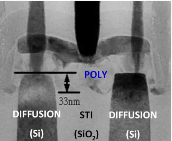
for 30nm nominal STI-oxide recess depths. ………
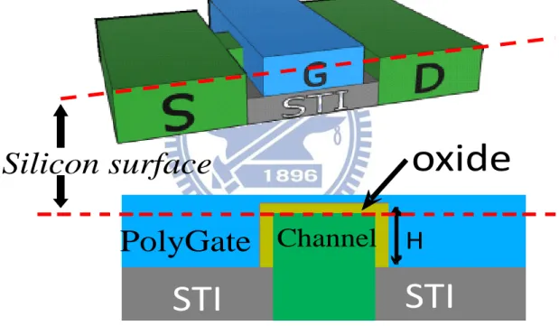
Fig. 3.4 (top) The 3D structure of bulk trigate formed by STI etching into the silicon
surface, to form the Fin-channel; (bottom) the cross sectional view with fin height H. Drain current is perpendicular to this plane. ………
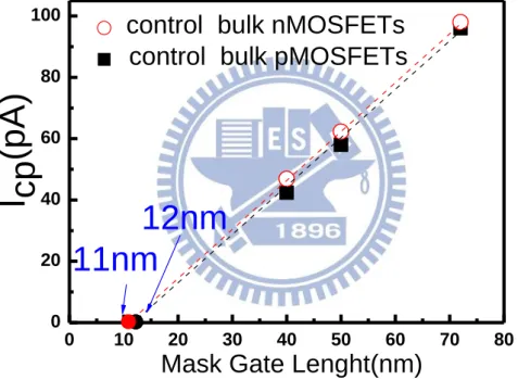
Fig. 3.5 The Leff in Table 2 can be extracted by the charge pumping measurement.
Leff= Lmask- L, L= 12nm (nMOS), 11nm (pMOS). ………
7 8 9 10 17 18 19 20 21
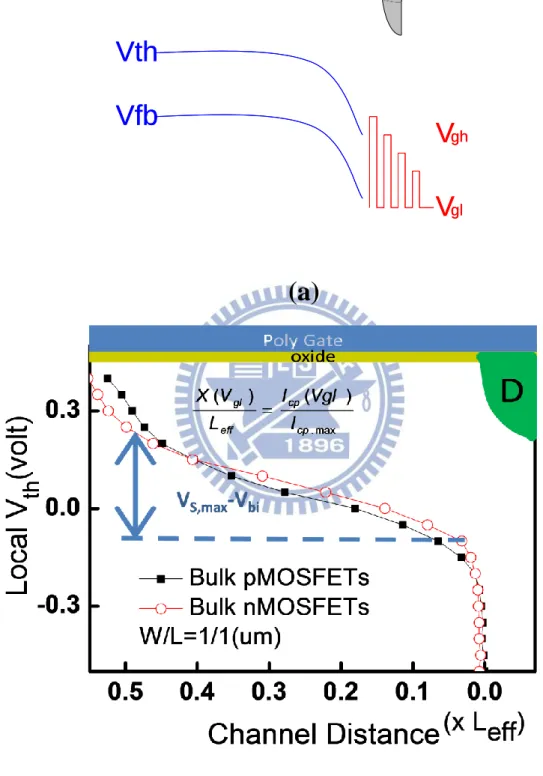
pumping measurement, the local threshold voltage can be profiled, where at the center (0.5Leff) the local threshold voltage reaches the maximum.……… Fig. 3.7 Vbi can be determined from Vth by varying Vbs, and the extrapolated value at
zero gate length yields to 2(Vbi-
S) + Vds such that Vbi can be found. ……… Fig. 3.8 The trigate devices shows obvious lower slopes of Avt than the planar ones(control) because a stronger gate field in trigate tends to inhibit the discrete dopant induced RDF. ………
Fig. 3.9 Although trigate devices show good variability, they show much worse Vth
degradation after the stress than the control, resulting in an increase of Vth variation. ………
Fig. 3.10 The local Vth profiling results by RTP for planar devices. It was found that the peaks are near the drain edge of the devices after the HC stress. ………
Fig. 3.11 The local Vth profiling results by RTP for trigate devices. It was found that the peaks are not only near the drain edge but also in the channel region after the HC stress. ………
Fig. 3.12 The comparison of trap densities for planar and trigate devices after the HC stress, showing that the traps of trigate device are much larger than those of planar device. ………
Fig. 3.13 The local Vth profiling results by RTP for planar devices. It was found that a larger amount of traps was generated in the channel center and drain edge after NBTI stress. ………
Fig. 3.14 The local Vth profiling results by RTP for trigate devices. It was found that many peaks are observed after NBTI stress in the channel region, coming from the sidewall roughness. ………
22 23 24 25 26 27 28 29 30
Fig. 4.1 The 3D structure of bulk Trigate (a) and split of Fin height (b), to form the
Fin-channel the cross sectional view with fin height H. Drain current is perpendicular to this plane. ………
Fig. 4.2 Illustration of the comparison between (a) high Rsd (b) low Rsd, the total
length of the high device is 36nm (gate length) + 200nm (S/D), on the other hand, the total length of the low device is 36nm (gate length) + 60nm (S/D).
Fig. 4.3 Comparisons of measured output characteristics for low Rsd vs. high Rsd
bulk trigate MOS devices, ID-VD curve. ……… Fig. 4.4 Ntrap profiling by different stress condition, different gate voltage bias,
showing that the trap distribution is affected by the stress bias. ………
Fig. 4.5 Ntrap profiling by different stress condition, different drain voltage bias,
showing that the trap distribution is affected by the stress bias. ………
Fig. 4.6 Illustration of S/D series resistance giving rise to a decrease in the effective
drain voltage as well as the lateral channel field for a given external drains bias. ………
Fig. 4.7 The threshold voltage degradation in (a) low electrical field and (b) high
electrical field, which show obvious serious Vth degradation in Trigate
devices. ………
Fig. 4.8 Ntrap profiling for different Rsd trigate devices after NBTI stress. By
increasing the resistance, the reliability was enhanced by high Rsd.………… Fig. 4.9 Illustration of the high electric field distribution at the corner and drain
edges for trigate which will induce the RTF for devices after the HC stress.
Fig. 4.10 Ntrap profiling results by RTP for low electric field condition. It was found
that the peaks are not only near the drain edge but also in the channel region after the HC stress. ………
Fig. 4.11 Ntrap profiling results by RTP for high electric field condition. It was found
that the peaks are not only near the drain edge but also in the channel region 40 41 42 43 44 45 46 47 48 49
Fig. 4.12 Illustration of the high electric field at the low fin height device which will
induce the higher electric field for devices by the HC stress. ………
Fig. 4.13 Ntrap profiling for different Fin-height trigate devices after the HC stress.
More traps are observed for lower Fin-height device as a result of larger electric field. ………
Fig. 4.14 Comparisons of transfer characteristics of P-channel trigate devices for two
different fin height values. ………
Fig. 4.15 To study the sidewall effects on the degradation of stressed trigate devices,
three different sidewall devices were measured. ………
Fig. 4.16 Ntrap profiling for different Fin-height Trigate devices after the NBTI stress.
More traps are observed for larger fin-height device as a result of sidewall roughness effect. ………
Fig. 4.17 Different fin spacing affects the variation of fresh devices. ………
Fig. 4.18 To study the fin spacing effect on the degradation of stressed trigate devices,
three different spacing devices were measured. ………
Fig. 4.19 Illustration of the STI spacing induced the sharper corner, such that higher
electric field at the corner was induced. ………
Fig. 4.20 Interface state density of Fin structure was measured by fabricating trigate
devices with RTP method, from Fin height dependency, Ntrap of 3.1x10¹⁰ (#/cm2) for top surface were extracted. ………
Fig. 4.21 10-year lifetime predictions of trigate pMOS devices after the NBTI stress,
showing the higher fin device shows poorer lifetime. ………
51 52 53 54 55 56 57 58 59 60
Table Captions
Table 3.1 The comparison of the generated trap densities for trigate and planar devices
after HC or NBTI stress, showing that NBTI stress dominates the reliability of trigate devices due to the surface roughness and corner effect of sidewall.
Table 4.1 The comparison of the generated trap densities in the middle of the channel
and near the drain edge after HC stress, showing that the damages near drain edge dominates the reliability of trigate devices in high electric field.………
Table 4.2 The comparison of the generated trap densities for different fin height
devices after NBTI stress, showing that fin height dominates the reliability of trigate devices due to the surface roughness. ………
32
61
Chapter 1
Introduction
1.1 Background
As the scaling of bulk CMOS devices reaches the physical limit, multi-gate device, or FinFET-like transistor structures, emerges as a promising candidate to extend its further scaling owing to its superior integration, higher subthreshold slope, reduced leakage, and immunity to the RDF (Random-Dopant Fluctuation) [1.1] by using the lightly-doped or undoped silicon fin. For ultra-low-power applications such as portable devices, implanted medical instruments, and wireless body sensing networks, operating at below threshold voltage is an effective solution [1.2] to reduce both static and dynamic power consumptions. Moreover, FinFET devices present the following advantages: (1) shallow trench isolation is not needed and (2) the device DIBL or short channel effect can be effectively improved as a result of the increasing gate controllability upon the channel region in the ultra-thin silicon body of Si-fin.
In reported studies, several reliability issues for FinFET have been identified, e.g., threshold voltage instability [1.3], stress induced film degradation [1.4], and corner effects
[1.5]. Among them, threshold voltage instability is due to the dynamics of carriers charging/discharging in oxide traps such as negative bias temperature instability (NBTI) in pMOS devices or hot carrier effect (HCE) in nMOS devices.
dopant fluctuation (RDF) is the major source of Vth variation in scaled bulk CMOS. To
improve the RDF, FDSOI or FinFET with undoped (lighter) channel [1.7-1.9], has been proposed subsequently to reduce the variability effectively.
Also, recent developments [1.10] in CMOS technology have highlighted the need in using the 3D technique as a method to extend the scaling of CMOS device for high speed and low power logic applications. Several approaches among them, such as tri-gate devices, double-gate devices, and FinFETs, along with lightly-doped or undoped silicon fin technology, have been utilized to improve the device performance. However, so far, the sources and the mechanisms of Vth variation have not been experimentally clarified on trigate devices. As a
consequence, we are interested in understanding the variability of trigate devices.
For the first time, in this thesis, we apply a new measurement method to observe the Vth variation in various n-MOS devices and p-MOS devices employing different channel area bulk trigate devices. The impact of the 3D device on the device reliability and variability will be investigated and compared.
1.3 Organization of the Thesis
There are five parts in this thesis. Chapter 1 is the introduction. In Chapter 2, we describe the experimental setup and the method of Methodology of Random Trap Profiling Technique (RTP). In Chapter 3, the variability study based on the Vth variation and the stress-induced
interface traps on n-MOS devices will be examined. On the other hand, using similar analysis, we will discuss the variability of trigate p-MOS devices. In Chapter 4, we will discuss the corner effect and sidewall surface roughness effect. Finally, the summary and conclusion will
Chapter 2
Experimental Setup and V
thVariation
2.1 Introduction
As devices are scaled to the nanoscale dimension, it is important to understand random fluctuations. Since there are many possible microscopic causes, it is desirable to understand the mechanism of variability. Therefore, electrical measurement of random fluctuations is a useful technique to observe such microscopic effects. It is necessary to collect a lot of data of standard deviation values for various kinds of transistors fabricated by different process conditions. If such data is properly compared and analyzed, it may become possible to extract quantitative information about random fluctuations. Based on this consideration, a simple normalization method for comparing standard deviation values of random threshold voltage fluctuations was proposed. The method was used to compare devices with various origins and to analyze the causes of random fluctuations [2.1].
This chapter is divided into two sections. First, we will illustrate the fundamental experimental setup to characterize CMOS devices. Second, the method of Random Trap Profiling Technique (RTP) used in this thesis will be introduced, and its fundamental theory will be described in detail.
2.2 Experimental Setup
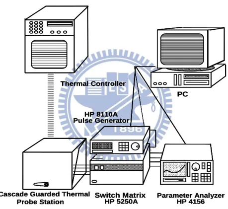
The experimental setup for the current-voltage measurement of devices is illustrated in
Fig. 2.1. Based on the PC controlled instrument environment by HP-IB (GP-IB, IEEE-488 Standard) interface, the complicated and long-term characterization procedures during analyzing the behaviors in MOS devices can be easily achieved. As shown in Fig. 2.1, the equipment, including the semiconductor parameter analyzer (HP 4156C), low leakage switch mainframe (HP E5250A), dual channel pulse generator (HP 8110A), cascade guarded thermal probe station and a thermal controller, provides an adequate capability for measuring the device characteristics. In addition, programs written by HT-Basic were used to execute the measurement via HP-IB interface.
2.3 Methodology of Random Trap Profiling Technique (RTP)
First of all, the amount of increased traps (Nit) can be extracted by standard deviation of
Vth, we know that the interface trap is the principal cause of the Vth shift if traps are
distributed discretely in the oxide,
D C q V V V V trap ox fresh th, shift th, fresh th, stress th, (1)
where Vth,stress is the threshold voltage after the stress by hot carrier or negative bias
temperature instability test. Vth,fresh and Vth,shift are the virgin threshold voltage and the shift
threshold voltage, respectively. Dtrap is the interface trap density. Also,
fresh
th,
2
σV
stress
th,
2
σV
shift
th,
σV
(2)and the result can be presented as the summation of the delta function of the trap density from the surface to the depletion region by a delta function, i.e.,
LW
)
(
)
(
dep W 0 ,
dx
x
N
C
q
D
C
q
V
trap ox trap ox shift th
(3) dep w trap trap 0 ox ΔN (x)δ(x x )dx q C LW
(4)W
L
)
(x
ΣΔN
C
q
eff trap trap ox
(5)L
ΔN
C
q
eff trap ox
. (6)From the above equations, we can obtain the interface trap density,
.
)
/cm
(#
)
σV
q
C
(
L
ΔN
2 2 shift th, OX eff trap
(7)Since RTF above the channel barrier peak dominates Vth variation after stress, the delta
trap density can be profiled along the channel as the peak shifted by varying the source-to-drain bias, Vsd. The principle of the measurement method is to locate the channel
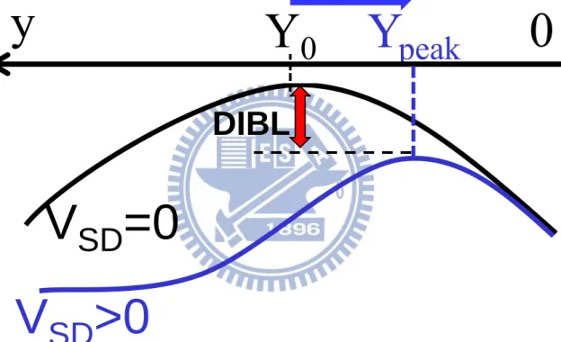
barrier peak position by varying the drain bias based on a quasi-2D Vth model (Fig. 2.2).
Because DIBL is proportional to the peak position which can be calculated by an analytic form [2.2] (Fig. 2.3), the peak position can be determine ed by the measured DIBL while the channel barrier was approximated as the second degree curve (Fig. 2.4), i.e.,
DIBL
Y
the junction barrier of the source and channel. The subthreshold swing can be expressed as dm OX
C
S.S.
(1
) 60mV
C
[2.3] (9)where Cox is the oxide capacitance, and Cdm is the depletion-layer capacitance given by
V
Q
C
dm
dep (10)the depletion capacitance is proportional to the channel length, because Qdep=qnLW. Then, we
can derive the following:
eff dm eff dm,0 0
L
ΔL
C
60
,
L
C
60
S.S.
mV
S.S.
mV
(11)from which the horizontal position along the channel is given by:
.
L
]
60mV
S.S.
60mV
-S.S.
)
V
-(V
DIBL
2
1
-2
1
[
Y
eff 0 max s, bi peak
(12)In the measurement method, the parameters were extracted experimentally. Leff can be
extracted by the charge pumping technique that our group developed in [2.4]. By applying continuous incremental pulses at the gate, the charge pumping current (Icp) is induced, then
the Icp will be proportional to the shape of the local Vth. Thus, the channel barrier height,
Vs,max, can be found. Vbi can be determined from Vth by varying Vbs, and the extrapolated
HP 8110A Pulse Generator
Cascade Guarded Thermal Probe Station
Switch Matrix
HP 5250A Parameter AnalyzerHP 4156
PC
Thermal Controller
Fig. 2.1 The experimental setup and environment for basic I-V measurement of MOSFET’s.
HP 8110A Pulse Generator
Cascade Guarded Thermal Probe Station
Switch Matrix
HP 5250A Parameter AnalyzerHP 4156
PC
Thermal Controller
HP 8110A Pulse Generator
Cascade Guarded Thermal Probe Station
Switch Matrix
HP 5250A Parameter AnalyzerHP 4156
PC
Thermal Controller
Fig. 2.1 The experimental setup and environment for basic I-V measurement of MOSFET’s.
Fig. 2.1 The experimental setup for the current-voltage measurement of MOS devices.
Automatic controlled characterizations system is setup based on the PC controlled instrument environment. The energy band diagram of the Si-SiO2 interface in the
Fig. 2.2 By varying the VSD, the barrier peak can be found from the DIBL since as VSD
increases, the barrier peak will be shifted toward the drain such that the delta trap density can be profiled along the channel.
Y
0
Y
peak
V
SD
>0
V
SD
=0
y
0
Fig. 2.3 It was found that the DIBL shift is well matched with the position of channel
barrier peak calculated by the analytical model.
0.0 0.4 0.8 1.2 1.6 2.0 2.4 2.8 0 2 4 6 8 10 12 Drain edge
DIBL
Position of Barrier Peak caculated by anayltic eaution
Gate Voltage (volt)
Pe
ak Po
siti
on
o
f Ch
an
ne
l Ba
rri
er (
nm)
nMOSFETs W/L=0.1 Channel center 0 40 80 120 160DIB
L(mV)
Fig. 2.4 A new model is to approximate the channel barrier as a second degree curve, in which
the peak position can be determined by the DIBL.
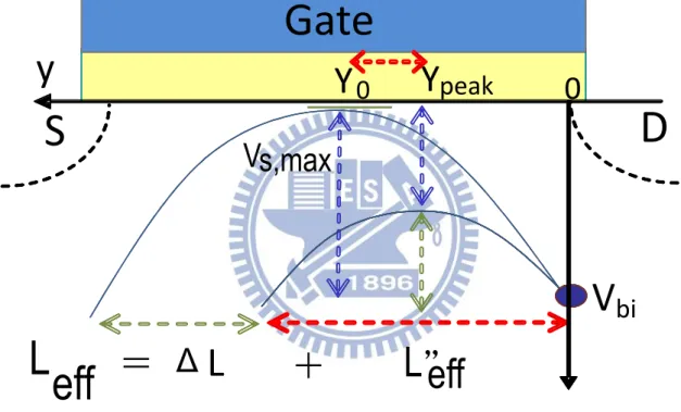
Gate
S
D
y
Δ
L
L”
eff
Leff
V
bi
0
Vs,max
Y
0
Y
peak
+
=
Chapter 3
Spatial Distribution of Traps in Bulk Trigate Devices
After Long Term Stress
3.1 Introduction
Bulk trigate devices might be the mainstream CMOS architecture beyond 20nm owing to good short channel effect and low Vth variation [3.1]. But, the reliabilities are rarely discussed,
and the discussion on the mechanism of degradation of such devices after the stress was very few. Doping and trap induce significant characteristic fluctuations [3.2] randomly in nanometer scale metal-oxide-semiconductor field effect transistors (MOS devices). The oxide trap spatial spectrum is the key to understand the mechanisms of degradation. Due to the ultra-scaled active region and multi-fin layout for trigate devices, we face the challenges to identify the oxide trap positions after the stress by the matured techniques, such as charge pumping technique [3.3], which is limited by small area devices. Since the order of the measured Icp is close to the background leakage, a new method should be urgently required. From reported results, it was found that Vth variation is dominated by discrete dopants at the
channel barrier peak, known as random dopant fluctuation (RDF). Furthermore, if oxide traps are present above the channel barrier peak, another effect, called random trap fluctuation (RTF) [3.4], will be involved in the Vth variationFig. 3.1. Therefore, the main idea of random
trap profiling technique is to measure Vth variation after the stress to identify the amount and
position of traps in bulk tri-gate devices which will then be extended to understand the physical mechanism associated with the fin-height.
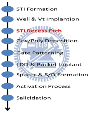
fabricated [3.5]. The bulk CMOS process, using the front-end-of-line steps outlined in Fig. 3.2. After the conventional STI process, good formation, and VT-adjust ion implantation, the
STI oxide was slightly recessed by various amounts on selected wafers prior to gate-stack formation. The schematic cross section diagram of a trigate MOS device is shown in Fig. 3.3. The width of trigate is 30nm and the height is different by recessed depth. Leff= 25nm. Both
control and splits are made on the same wafer. To exclude and avoid the parasitic effects, single-fin devices were prepared, Fig. 3.4. Devices with different areas were used to calculate the Vth variations.
3.3 Parameters of the Measurement Method
In the measurement method, the parameters were extracted experimentally (Fig. 3.5- 3.7), Leff can be extracted by the charge pumping technique on the control devices simultaneously
made on the same wafer. When the continuous increment pulses reached over the local threshold voltage (Vth) and local flat band voltage (Vfb), the charge pumping current (Icp)
begins conduction, then the Icp will be proportional to the shape of local Vth. Thus, the channel
barrier height can be found. Vbi can be determined from Vth by varying Vbs, and the
extrapolated value at the gate length vanishes will be a function of Vbi.
3.4 Variability of Trigate MOS Devices
First of all, bulk trigate devices improve Vth variation because stronger gate electrostatic suppresses RDF, thefactorAvt [3.6] has a linear relation with channel area, which can help us
to understand the fluctuation of electrical characterizing in different channel areas, as shown in Fig. 3.8. Here, the trigate devices shows obvious smaller slopes of Avt than the control ones
induced RDF. But, after the stress, Vth degradation of trigate devices was much worse than
that of control due to RTF (Fig. 3.9).
3.5 Impact of Stress-induced Random traps
3.5.1 Introduction
A large number of variation effects have been reported, examples include: random dopant fluctuation (RDF) [3.7], line-edge roughness (LER) [3.8-3.9], and local oxide thickness variations [3.10]. In addition to these effects, recent study [3.11] has proved that process-induced random traps fluctuation (RTF) is required for proper interpretation of Vth
variation in CMOS technologies. However, so far, none has been reported on the effect of stress-induced random interface traps. Thus, in this section, we will discuss the device variability after the HC stress.
3.5.2 Variability After the HC Stress
Since the positions and number of charges trapped at the SiO2/Si interface are randomly
distributed, it is possible for this variation to affect the Vth variation [3.12]. Fig. 3.10shows the
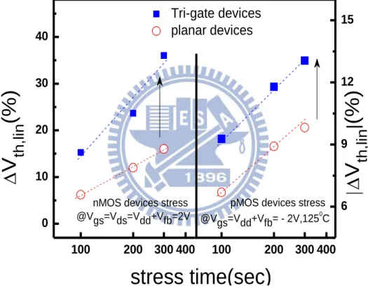
measured Vth for studying the stress effect using the HC stress (VGS= VDS= Vdd+Vfb= 2V for
100 and 200sec) on planar n-MOS device. It is observed that standard deviation of the devie after the stress is larger than that of the fresh device, because the standard deviation of stressed device contains Random Dopant Fluctuation (RDF) and Random Trap Fluctuation (RTF) and
found that the peaks are near the drain edge of the devices after the HC stress, but for the local Vth profiling results of trigate devices, it was found that the peaks are not only near the drain
edge but also in the channel region after the HC stress. Fig. 3.11
This result indicates that stress-induced interface traps are the dominant source of the enhanced Vth variation after the HC stress, and the planar and trigate device contains different
factors inducing Vth.
3.5.3 Variability After the NBTI Stress
By applying a similar analysis, we apply the NBTI stress (VGS -Vth= -2V at 125℃) to
generated the interface traps of the pMOS device which would show more degraded Vth
variation. To study the stress-induced degradation, Fig. 3.13 shows the measured the standard deviation after the NBTI stress (VGS -Vth= -2V for 100 and 200sec, at 125℃). The standard
deviation of trigate device is larger than that of the planar device. The result indicates that trigate generates more interface traps at the SiO2/Si interface in comparison to the planar device.
Fig. 3.14 shows the local Vth profiling results by RTP for trigate devices. It was found that
many peaks are observed after NBTI stress in the channel region, originating from the sidewall roughness. (Fig. 3.15) The trap densities of trigate devices are much larger than those of the control.
.
The result is similar to that of n-MOS devices, in which we observed a higher standard deviation in trigate device after the NBTI stress that is attributed to the more interface traps generation.
3.5.4 Discussion
To characterize the oxide trap spatial spectrum, random trap profiling was performed after the hot carrier (HC) stress on the planar and trigate nMOS devices respectively. (Fig. 3.10~12) It was found that the local Vth variation fluctuated heavily near the drain edge after the HC stress, showing where the traps were generated due to a high electric field. (Fig. 3.10) But, for trigate devices after the HC stress(Fig. 3.11), not only the local Vth variation was observed near drain edge but also on the sidewall, meaning that the sidewall is a critical region in terms of trigate reliability. We suspect that the sidewall corner effect induced a high electric field, consequently generating the traps. As a result, in trigate nMOS device, the trap density calculated from Vth was much higher than that of the planar after the HC stress. (Fig.
3.12)
NBTI stress was also applied to examine the degradations of the planar and bulk trigate pMOS devices. (Fig. 3.13~Fig. 3.15) In planar devices, local Vth variation occurred around
the channel center. (Fig. 3.13) But, for trigate devices, unusual peaks of local Vth variation
(blue lines) were observed in the channel region. (Fig. 3.14) We assume that these peaks came from the traps caused by the surface roughness and corner effect of the sidewall. Because, during NBTI stress, the profile of electric field intensity distributed across the sidewall, and the closer to corner the field is, the stronger the intensity becomes. This high intensity field led to the generation of traps. So the trap densities of trigate devices were much larger than those of the control. (Fig. 3.15)
Fig. 3.1 Vth variation is dominated by the discrete dopants in the channel, known as RDF;
however, after the stress, another effect, RTF caused by the traps, will also lead to Vth variation.
Gat
e oxide
D
S
chann
el
Oxide traps
Discrete
dopants
Fig. 3.3 Transmission electron microscopy cross-section taken along a poly-Si gate for
Fig. 3.4 (top) The 3D structure of bulk trigate formed by STI etching into the silicon
surface, to form the Fin-channel; (bottom) the cross sectional view with fin height H. Drain current is perpendicular to this plane.
STI
Channel
PolyGate
H
oxide
STI
Silicon surface
Fig. 3.5 The Leff in Table 2 can be extracted by the charge pumping measurement. Leff=
Lmask- L, L= 12nm (nMOS), 11nm (pMOS).
0 10 20 30 40 50 60 70 80 0 20 40 60 80 100
12nm
I cp
(pA)
Mask Gate Lenght(nm)
control bulk nMOSFETs
control bulk pMOSFETs
(a)
(b)
Fig. 3.6 (a) Illustration of the flat-band and local threshold voltages, (b) Using charge
pumping measurement, the local threshold voltage can be profiled, where at the
D
GateVth
Vfb
V
glV
ghVth
Vfb
V
glV
ghFig. 3.7 Vbi can be determined from Vth by varying Vbs, and the extrapolated value at zero
gate length yields to 2(Vbi-
S) + Vds such that Vbi can be found.0 10 20 30 40 50 60 70 80 1E-3 0.01 0.1
V
th
(v
o
lt
)
Gate Length(nm)
V
BS=0V
V
BS=-0.5V
V
BS=-1V
Control nMOSFETs
0.05V
@V
)
(
2
ds
s
ds
bi
V
V
Fig. 3.8 The trigate devices shows obvious lower slopes of Avt than the planar ones
(control) because a stronger gate field in trigate tends to inhibit the discrete dopant induced RDF. 1 2 3 4 5 0 2 4 6 8 10
12 planar nMOS devices
tri-gate nMOS devices planar pMOS devices tri-gate pMOS devices
V
th
(mV
)
1/LW (um
-1)
Avt
nMOS
pMOS
Fig. 3.9 Although trigate devices show good variability, they show much worse Vth
degradation after the stress than that of the control, resulting in an increase of Vth variation. 100 200 300 400 0 10 20 30 40 100 200 300 400 6 9 12 15
pMOS devices stress @Vgs=Vdd+Vfb= - 2V,1250C
V
th
,l
in
|
(%
)
Tri-gate devices planar devicesstress time(sec)
V
th
,l
in
(%
)
nMOS devices stress @Vgs=Vds=Vdd+Vfb=2V
Fig. 3.10 The local Vth profiling results by RTP for planar devices. It was found that the peaks are near the drain edge of the devices after the HC stress.
2 4 6 8 10 12 14 0 3 6 9 12 15
Position(nm)
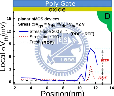
Stress time 200 s Stress time 100 s Freshplanar nMOS devices
Stress @Vgs = Vds =Vdd+Vfb =2 V
Local
V
th
(mV)
oxide
Poly Gate
D
RTF RDF (RDF+ RTF) (RDF)Fig. 3.11 The local Vth profiling results by RTP for trigate devices. It was found that the peaks are not only near the drain edge but also in the channel region after the HC stress. 2 4 6 8 10 12 14 0 5 10 15
trigate nMOS devices
Stress @Vgs = Vds =Vdd+Vfb =2 V
Local
V
th(m
V)
Position(nm)
stress 200s stress 100s Freahoxide
Poly GateD
Fig. 3.12 The comparison of trap densities for planar and trigate devices after the HC stress, showing that the traps of trigate device are much larger than those of planar device. 3 6 9 12 0 2 4 6 8 10
Position
(
nm
)
N
tr a p(
10
12#/cm
2)
trigate nMOS devices planar nMOS devices
Stress @
Vgs = Vds =Vdd+Vfb =2 V,200s
oxide
Poly Gate
Fig. 3.13 The local Vth profiling results by RTP for planar devices. It was found that a larger amount of traps was generated in the channel center and drain edge after NBTI stress.
oxide
Poly Gate
Fig. 3.14 The local Vth profiling results by RTP for trigate devices. It was found that many peaks are observed after NBTI stress in the channel region, coming from the sidewall roughness.
3
6
9
12
0
1
2
3
4
5
Local
V
th
(mV)
trigate pMOS devices
Stress @Vgs =Vdd+Vfb =-2 V, 125 0 C stress 200 s stress 100 s fresh
Position(nm)
oxide
Poly Gate
D
Fig. 3.15 The trap densities of trigate devices are much larger than those of the control. 0 3 6 9 12 15 0 2 4 6 8 pMOS devices Stress @Vgs = Vdd+Vfb =-2 V, 1250C
N
tr a p(
10
10#
/cm
2)
Position(nm)
0 20 40 60 80
N
tr a p(
10
10#
/cm
2)
planar devices trigate devicesoxide
Poly Gate
D
Table 3.1 The comparison of the generated trap densities for trigate and planar devices after
HC or NBTI stress, showing that NBTI stress dominates the reliability of trigate devices due to the surface roughness and corner effect of sidewall.
Average Increased Trap Density(cm
-2
)
Bulk Planar
Devices
Bulk Trigate
Devices
HC stress
@ V
gs=V
ds=
V
dd+V
fb, 25
0C, 200sec
NBTI stress
@
V
gs=V
dd+V
fb,125
0C,200sec
Splits
Stress
Condition
8
Chapter 4
Experimental Observation on the Trap Fluctuation of
Small Scale Trigate CMOS Devices
4.1 Introduction
Trigate is a promising structure for MOS transistors with gate lengths of 20 nm and smaller. Several variants of the gate design in trigate device have been suggested [4.1]. In the trigate case, the gate wraps around the rectangular silicon fin from three sides. The Trigate device has a large effective channel width: Weff= 2*Tfin + Wfin. So, the use of the gate wrap
around design is attractive since a significantly higher drive current can be achieved for the same minimum feature size.
In this chapter, we will demonstrate that Vth variation can be suppressed by advanced 3D
technology meanwhile the performance of devices keeps improved for MOS devices. Extensive comparisons between trigate and segmented trigate devices will be justified on examining the effects of electrical field and sidewall height [4.2]. In addition, the impact of corner effects on the device variability will also be verified [4.3]. The comer effect which is known to make worse the electrical performance of the shallow trench isolated (STI) MOS transistors [4.4-5]. In this chapter, we will examine the comer effect on the electrical performance of trigate transistors with minimum feature size of 36 nm.
impact-ionization at the corner of the sidewall but also the surface roughness at the sidewall need to be taken care of. Therefore, this study will investigate the effect of varying sidewall height in the trigate devices.
4.2 Device Preparation
Advanced poly-Si gate bulk trigate devices, with SiON insulator, were fabricated. After the conventional STI process, well formation, and VT-adjust ion implantation, the STI oxide
was slightly recessed by various amounts (10nm, 15nm, or 30nm) on selected wafers just prior to gate-stack formation. The schematic cross section diagram of trigate MOS device splits are shown in Figs. 4.1-4.2. Also, the electrical characteristics are given in Fig. 4.3, where the driving current of low S/D resistance trigate device is larger than the low Rsd ones.
The width of trigate is 45nm and the height is different by recessed depth. The effective channel length, Leff= 25nm for n type and Leff= 24nm for p type devices. Both control and
split are made on the same wafer. To exclude and avoid the parasitic effects, single-fin devices were prepared. Devices with different areas were used to calculate the Vth variations.
4.3 Factors Affecting the Reliability in Trigate nMOSFET
4.3.1 Stress voltage bias dependence
To characterize the oxide trap spatial distribution, random trap profiling was performed after hot carrier (HC) stressing the trigate nMOS devices. (Figs. 4.4-4.5) By changing the vertical electric field, it was found that the density of trap becomes larger near the drain edge
electric field. On the other hand, by changing the lateral electric field, it was found that the region of the distribution of trap, and the density of trap was not increased more heavily by the stress. We suspect that the electric field was controlled by the bias voltage.
4.3.2 S/D Resistance dependence
In this part, we will investigate the threshold voltage degradation characteristics of the
fabricated high and low S/D resistances,Fig. 4.2, respectively. Gate length (Lg) for device is
36 nm, and effective channel length (Leff) is 25 nm. Owing to the surrounding-gate structures,
healthy switching characteristics are obtained even at low S/D resistance device [4.7-8]. An increment of S/D series resistance gives rise to a decrease in the effective drain voltage (V’D
=VD – 2*ID*(RS/D + Rext) as well as the lateral channel field for a given external drain bias
(Fig. 4.6). Under the hot carrier stress, the degradation of Vth is largely increased for low
resistance device, because the device contain larger electric field; on the other hand, the electric field of high resistance device was smaller, because there is a voltage drop across the source/drain series resistance. Therefore, the surface roughness effect for low S/D resistance device is much worse than the high S/D resistance device. The results are shown inFig. 4.7
and Fig. 4.8.
4.3.3 Corner effect
of the high electric field at the trigate corner in Fig. 4.9 will induce the RTF for devices after the HC stress. It can be seen that the current flow is pushed toward the corners in the case of trigate MOS device (2-corner effect). The issue causes slightly higher local standard deviation of threshold voltage which is produced by interface traps.
First, we measured hot carrier degradation in bulk trigate devices under the bias condition of VGS= VDS= 1.7 volt and 2.2 volt, because the worst stress condition at operating
voltage is VGS= VDS. In low electric field case, it shows that the degradation is dominated by
corner effect, Fig. 4.10, because the local Vth variations near the drain edge and middle of
channel are similar. On the other hand, we suspect that the sidewall corner effect induced a high electric field and generated the traps, but in Fig. 4.11 it shows that the degradation is dominated by the hot carrier. So, it was found that the dominated effect was different in varying electric field, especially deserved to be mentioned, the corner effect was found no matter whether the stress condition is.
4.3.4 Fin Height dependence under HC stress
As the stress bias is increased, the degradation of Vth is accelerated due to the
incremental change in the electric field. Larger degradation is observed at the shorter fin height rather than at the higher fin height under the same stress condition [4.9]. Due to the low fin height device, it will induce a higher electric field for devices after the HC stress,Fig. 4.12. The Ntrap profiling for different Fin-height trigate devices after HC stress is show in Fig.
4.4 Factors Affecting the Reliability in Trigate pMOSFET
4.4.1 Surface roughness
To enhance the driving current of the trigate MOS devices, the higher sidewall was evaluated. Fig. 4.14 is the change of driving current of the same trigate devices (equivalent effective length and gate width) when the sidewall depth increases up to 30 nm. To examine the sidewall effects, devices with three different sidewall heights have been compared, Fig. 4.15, in which the higher the sidewall is, the more device degradation becomes as a result of the sidewall roughness and a high electric field on the sidewall corner. As expected, the drive current of devices increase as the recess depth increases from 10 nm, 15 nm, and to 30 nm. Unfortunately, the variation of the trigate devices is larger when the height of the sidewall increased by process (Fig. 4.16). And, the threshold voltage was degraded in higher sidewall device. This means that the trigate MOS devices will suffer from serious variability problem without tight control of sidewall height. One way to handle this problem will be to use more controllable process.
4.4.2 The Shallow Trench Isolation effect
NBTI stress was also applied to examine the degradations of the trigate pMOS devices. To further identify the local Vth variation caused by the STI effect, we measured the fresh
region of FET near the STI beak has been suffered from the stress of the beak and induced the traps in the region. For narrow fin spacing devices that exhibit a sharp beak, Fig. 4.19, it induces higher electric field under the stress.
4.5 Discussion
As a result, in bulk trigate nMOS devices, the trap density was much higher than that of the convention trigate after the HC stress. Because the high electric field was induced by corner structure, so the damage becomes more serious for trigate devices. In addition, the influence of corner effect under varying electric field is summarized in Table 2. According to the measured data, we know that the average increased trap density near the drain edge was 2.18 times as large as the average increased trap density in the middle channel for low electric field case. On the other hand, the average increased trap density near the drain edge was 3.35 times as large as the average increased trap density in the middle channel for high electric field case, so the corner effect will dominate the reliability of segmented trigate devices for low voltage operation.
To examine the sidewall effects, devices with three different sidewall heights have been compared, Table 3, in which the higher the sidewall is, the more device degradation becomes as a result of the sidewall roughness and a high electric field at the sidewall corner.
In Fig. 4.20, the interface state density of Fin structure was measured by fabricating trigate devices with RTP method, from Fin height dependency, Ntrap of 3.1x10¹⁰ (#•cm-2) of top surface was obtained, meaning that NBTI stress dominates the reliability of trigate
pMOS devices after the NBTI stress. It shows that the higher the fin is, the device shows poorer lifetime,Fig. 4.21.
(a)
(b)
Fig. 4.1 The 3D structure of bulk Trigate (a) and split of Fin height (b), to form the
Fin-channel the cross sectional view with fin height H. Drain current is perpendicular to this plane.
STI
Channel
PolyGate
H
oxide
STI
Silicon surface
Cha nn el P oly S T I10nm
15nm
30nm
Cha nn el P oly S T I10nm
15nm
30nm
Cha nn el P oly S T I10nm
15nm
30nm
Fig. 4.2 Illustration of the comparison between (a) high Rsd (b) low Rsd, the total length of
the high device is 36nm (gate length) + 200nm (S/D); on the other hand, the total length of the low device is 36nm (gate length) + 60nm (S/D).
Fig. 4.3 Comparisons of measured output characteristics for low Rsd vs. high Rsd bulk
trigate MOS devices, ID-VD curve.
0.0 0.2 0.4 0.6 0.8 1.0 1.2 1.4 1.6 1.8 0 20 40 60 80 100
low S/D resistance devcies high S/D resistance devcies
V
DS
(V)
I d
(
A
)
nMOS trigate devices W/H/L=45/10/36 (nm) Vgs=Vth,lin +1 V
Fig. 4.4 Ntrap profiling by different stress condition, different gate voltage bias, showing
that the trap distribution is affected by the stress bias.
0.0 0.1 0.2 0.3 0.4 0.5 0 1 2 3 4 5 E = 6.2 MV/cm (Vgs=1.8V) E = 7.2 MV/cm (Vgs= 2V) E = 8.2 MV/cm (Vgs=2.2V)
N
tra
p
(10
12
#/cm
2
)
Channel Distance, unit in L
eff
E// = 0.83 MV/cm nMOS trigate devices W/H/L=45/30/36 (nm) Stress Time = 200 s
oxide
Poly Gate
Fig. 4.5 Ntrap profiling by different stress condition, different drain voltage bias, showing
that the trap distribution is affected by the stress bias.
0.0 0.1 0.2 0.3 0.4 0.5 0 1 2 3 4 5
Channel Distance, unit in L
eff
E = 7.2 MV/cm (Vgs=2V)
nMOS trigate devices W/H/L=45/30/36 (nm) Stress Time = 200 s
N
tra
p
(10
12
#/cm
2
)
E// = 0.75 MV/cm (Vds=1.8V) E// = 0.83 MV/cm (Vds= 2V) E// = 0.91 MV/cm (Vds=2.2V)oxide
Poly Gate
D
Fig. 4.6 Illustration of S/D series resistance giving rise to a decrease in the effective drain
voltage as well as the lateral channel field for a given external drains bias.
V
G
V
D
V
S
R
S/D
R
ext
R
S/D
R
ext
V’
D
= V
D
-2*I
D
(R
S/D
+ R
ext
)
(a)
(b)
Fig. 4.7 The threshold voltage degradation in (a) low electrical field and (b) high electrical
field, which show obvious serious Vth degradation in Trigate devices.
100 200 300 0 30 60 90 120
nMOS trigate devices Stress@Vgs = Vds = 1.7 V W/H/L = 45/10/36 (nm) low Rsd high Rsd
V
th, li n(%)
Stress Time (s)
20.2% 69.5% 100 200 300 0 50 100 150 200 250 300 350 low Rsd high RsdnMOS trigate devices Stress@Vgs = Vds = 2 V W/H/L = 45/10/36 (nm)
V
th, li n(%)
Stress Time (s)
99% 228%Fig. 4.8 Ntrap profiling for different Rsd trigate devices after NBTI stress. By increasing
the resistance, the reliability was enhanced by high Rsd.
0.0 0.1 0.2 0.3 0.4 0.5 0 2 4 6
N
tra
p
(10
12
#/cm
2
)
High Rsd device Low Rsd deviceChannel Distance, unit in L
eff
nMOS device Stress W/H/L = 45/10/36 (nm) Stress Time = 200 s @E=7.2 MV/cm E//= 0.83 MV/cm (Vgs=Vds=2 V)
oxide
Poly Gate
D
Fig. 4.9 Illustration of the high electric field distribution at the corner and drain edge for
Fig. 4.10 Ntrap profiling results by RTP for low electric field condition. It was found that
the peaks are not only near the drain edge but also in the channel region after the HC stress. 0.0 0.1 0.2 0.3 0.4 0.5 0.0 0.5 1.0 1.5 2.0 2.5 3.0
nMOS trigate devices W/H/L = 45/30/36 (nm) Stress Time = 200 s
N
tra
p
(10
12
#/cm
2
)
E5.7 MV/cm
E//=0.7 MV/cm
(Vgs=Vds=1.7V )
Channel Distance, unit in L
eff
oxide
Poly Gate
Fig. 4.11 Ntrap profiling results by RTP for high electric field condition. It was found that
the peaks are not only near the drain edge but also in the channel region after the HC stress. 0.0 0.1 0.2 0.3 0.4 0.5 0.0 0.5 1.0 1.5 2.0 2.5 3.0
nMOS trigate devices W/H/L = 45/30/36 (nm) Stress Time = 200 s
N
tra
p
(10
12
#/cm
2
)
E8.2 MV/cm
E//=0.91 MV/cm
(Vgs=Vds=2.2V )
Channel Distance, unit in L
eff
oxide
Poly Gate
Fig. 4.12 Illustration of the high electric field at the low fin height device which will induce
the higher electric field for devices by the HC stress.
30nm
10nm
channel
More concentrative
of the field
Fig. 4.13 Ntrap profiling for different Fin-height trigate devices after the HC stress. More
traps are observed for lower Fin-height device as a result of larger electric field.
0.0 0.1 0.2 0.3 0.4 0.5 0 1 2 3 4 5
N
tra
p
(10
12
#/cm
2
)
nMOS trigate devices L= 36 nm W= 45 nm
Stress@Vgs=Vds= 2 V, 200 s
Fin height = 10 nm Fin height = 15 nm Fin height = 30 nm
Channel Distance, unit in L
eff
oxide
Poly Gate
Fig. 4.14 Comparisons of transfer characteristics of P-channel trigate devices for two
different fin height values.
-1.6 -1.4 -1.2 -1.0 -0.8 -0.6 -0.4 -0.2 0.0 0.2 0.4
-0.5 0.0 0.5 1.0 1.5 2.0 2.5 3.0 3.5 4.0 4.5 5.0Fin Height 10 nm
Fin Height 30 nm
pMOS device W= 45 nmI
d
(
A
)
Gate Bias (V)
Fig. 4.15 To study the sidewall effects on the degradation of stressed trigate devices, three
different sidewall devices were measured.
PolyGate
PolyGate
PolyGate
Channel
Channel
Channel
STI
STI
STI
(a)
(b)
(c)
oxide
10nm
15nm
30nm
Fig. 4.16 Ntrap profiling for different Fin-height Trigate devices after the NBTI stress. More
traps are observed for larger Fin-height device as a result of sidewall roughness effect. 0.0 0.1 0.2 0.3 0.4 0.5 0 3 6 9 12 15 Fin Height=10nm Fin Height=15nm
pMOS trigate devices, W/L= 45/36 (nm)
Stress @Vgs = Vdd+Vfb =-2 V, 125
0
C