ELSEVIER Materials Chemistry and Physics 44 (1996) 95-99
Materials Science Communication
Uniformity of epilayer grown by ultrahigh-vacuum chemical
vapor deposition
Ting-Chang Chang”>*, Wen-Kuan Yehb, Chun-Yen Changb, Tz-Guei Jungb,
Wen-Chung Tsai b, Guo-Wei Huangb, Yu-Jane Meib
aNational Nano Device Laboratory, 1001-l Ta-Hsueh Rd., Hsinchu 300, Taiwan, ROC
bDepartment of Electronics Engineering and Institute of Electronics, National Chino Tung University, 1001 Ta-Hsueh Rd., Hsinchu 300, Taiwan, ROC
Received 19 December 1994; accepted 7 July 1995
Abstract
In this work, we explored the Ge fraction, layer thickness and dopant concentration uniformity of epilayers grown by an ultrahigh-vacuum chemical vapor deposition system (UHVjCVD). Three epilayers were grown for this study: a single epilayer of SiGe, a heavily boron doped Si epilayer and a Si/SiGe superlattice with p+ Si cap. The uniformity in a wafer was measured to be less than f 1.5%. In addition, we explored the wafer-to-wafer uniformity of a strained SiGe layer. The variations in thickness and composition between two samples grown in the same run were evaluated to be f 1.3 and j! 1.2%, respectively. These results show that uniform layers can be simultaneously obtained on many wafers by the UHVjCVD system.
Keywords: Epilayers; Ultrahigh-vacuum chemical vapor deposition system; Uniformity
1. Introduction
In recent years, research into the growth of strained- layer superlattices (SLS) has greatly stimulated the development of heteroepitaxy, because of its possible applications in bandgap engineering. The Si/Si, --x Ge, heterostructure has been studied extensively and new devices based on this material system have been pro- posed and fabricated [l-7].
For advanced Si/SiGe device fabrication, a low-tem- perature process is desirable for minimizing problems associated with lattice mismatch and interdiffusion. The UHVjCVD system is an important technique for low- temperature growth of Si and SiGe epitaxial layers. A particular advantage of this growth technique is the fact that uniform layers can be obtained on many wafers simultaneously. As a result, the growth technique is
* Corresponding author.
0254-0584/96/$15.00 0 1996 Elsevier Science S.A. All rights reserved
readily usable in manufacturing. Other alternative tech- niques for SiGe growth, such as molecular beam epi- taxy (MBE), limited reaction process (LRP), or atmospheric pressure epitaxy, are usually performed in single wafer reactors. Recently, Greve et al. have inves- tigated the uniformity of SiGe epitaxial layers grown by UHV/C!VD [S]. However, only the uniformity of SiGe epilayer was studied in their work. In this work, we study the Ge fraction, layer thickness and dopant con- centration uniformity of epilayers grown by the UHV/ CVD system. These epilayers include a single epilayer of SiGe, a heavily boron doped Si epilayer and a Si/SiGe superlattice with p+ Si cap.
2. Experimental
Three samples were grown on 3-in., (001) Si sub- strates using a home-made hot-wall multiwafer UHV/ CVD system for this study. They are a single epilayer of
96 T.-C. Gang et al. /Materials Chemistry and Physics 44 (1996) 95-99 SiGe, a heavily boron doped Si epilayer and a Si/SiGe
superlattice with p+ Si cap. In this work, the growth
temperature was kept constant at 550 “C. Prior to
the growth, the substrate was subjected to an H,SO,: H,O, = 3: 1 clean and a 10% HF dip. Silane ( SiH,) and
10% germane (GeH,) in hydrogen were used as reac-
tant gases. In addition, 1% diborane (B2H6) in hydro-
gen was used as the p-type dopant gas. The base
pressure of the system was maintained at about
2 x IO-* torr in the growth chamber. During growth,
the system was operated at about 1.0 mtorr. Layer
uniformity was evaluated by high-resolution double-
crystal X-ray (HRXRD). Variations in the layer com-
position were found by collecting rocking curves from
several locations spaced between the wafer edge
(r = 38 mm) and the wafer center (r = 0 mm). Data was
collected in four arcsec steps, with a count time of 18 s per step. The structural parameters were determined
from a comparison between the experimental rocking
curve and the simulated one.
3. Results and discussion
Fig. 1 shows the HRXRD (004) rocking curves ob-
tained from several locations in the 370 nm thick
Si 0,875Ge,,,,6 epilayer. Nearly identical rocking curves
were obtained, indicating good in-wafer uniformity in
thickness and Ge fraction. In the full-strained SiGe
case, the Ge composition x is directly related to the
peak splitting A9 by
x = A9jlO480 (1)
where A0 is expressed in arcsec. Thickness (t) was
determined using the period of intensity oscillations
(Pendelliisung fringes) between the layer and substrate
Sub
-2500 -2000 -1500 -1000 -500 0 500 1000
A@CseC)
Fig. 1. The HRXRD (004) rocking curves obtained from several locations of in about 370 nm thick Si,,,,,Ge,,,,, epilayer.
peaks (see Eq. (2)):
t = 3, sin 0,/A9 sin 2e8
where 6& is the Bragg’s angle of Si (004).
(2)
The variation in Ge composition versus distance
from the center of the wafer, r, is presented in Fig. 2.
The variation in Ge fraction is within +1.5%. In this
SiGe sample, no thickness variations were observed
within the experimental error ( +9 nm).
In order to study the uniformity of the dopant concen-
tration, a 250 nm thick Si-B epilayer with a boron
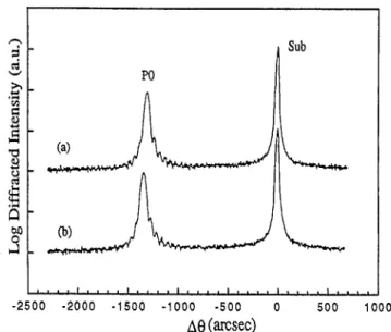
concentration of 8.1 x 10’” cms3 was used. Fig. 3 shows
the HRXRD (004) rocking curves obtained from several
locations of this heavily boron-doped Si epilayer. Simi- larly, nearly identical rocking curves are obtained, indi-
cating good in-wafer uniformity in thickness and boron
0’13
/
L
9 0.128
-
s
.I
2
0.126 - z ‘ii 0.124 - Q 0.122 - 0 10 15 20 25 30 35 40 r (mm)Fig. 2. The variation in Ge composition versus distance from the center of the wafer (r).
Sub
0 Afj(arcsec)
Fig. 3. The HRXRD (004) rocking curves obtained from several locations of a heavily boron-doped Si epilayer.
T.-C. Gang et al. /Materials Chemistry and Physics 44 (1996) 9.5-99 97
concentration. In a lightly doped epilayer, the distor-
tion of the lattice constant by the incorporation of a
dopant is negligible. However, the incorporation of a
dopant can strongly distort the lattice in a heavily doped epilayer [9, lo]. In Fig. 3, peak Sub and peak PO represent the reflection of substrate and Si-B epilayer,
respectively. Since the lattice constant of Si-B is
smaller than that of Si-Si, the peak PO appears on the high angle side of the substrate peak Sub. The boron
concentration can be determined by the angle separa-
tion between peak PO and peak Sub. The variation in
boron concentration versus distance from the center of
the wafer, Y, is demonstrated in Fig. 4. The variation in
boron concentration is about _+1.6%. The variation in
boron concentration is a little higher than that in the
Ge fraction. However, such observed variations were
within the experimental error ( &9 nm).
Fig. 5(a) shows the HRXRD (004) rocking curves
obtained from a Si/SiGe superlattice of 20 periods with Si-12 nm, SiGe-5.1 nm, 17.7% Ge, and boron doped Si cap layer (N = 1.12 x 10”’ cmw3)-96 nm. In this figure, peak Sub represents the Si substrate reflection, peak PO
the zeroth-order superlattice reflection, and the other
main peaks are satellite peaks ( -3, -2, - 1, + 1) re- sulting from the periodicity of the superlattice. In addi- tion, a broad peak labeled peak C on the right side of the substrate resulted from the p” Si cap, which is used to form an ohmic contact for the devices. Fig. 5(b) shows the simulated rocking curve for this Si, --x Ge, /Si superlattice. In this simulated rocking curve, we have considered the effect of diffused scattering from the first
crystal and substrate [ll]. As compared to Fig. 5(a),
excellent matches between experiment and simulation in
terms of peak position, peak intensity, and full width at
19
x10
10 ,
t
r (mm)
Fig. 4. The variation in boron concentration vs. distance from the center of the wafer (1.).
t I I I I I I A
-5Gol -5m 44xX -3ca -2m -IO00 0 loo0 2m
A6 (arcs=)
Fig. 5. (a) The HRXRD (004) rocking curves obtained from a Si/SiGe SLS of 20 periods with Si-12 nm, SiGe-5.1 nm, 17.7% Ge, and boron doped Si cap layer (N = 1.12 x 10” cmW3)-96 nm; (b) simulated rocking curve.
half maximum (FWHM) of each main peak are clearly
observed. Therefore, we can conclude that strained
Si/SiGe superlattice with excellent interfaces and crys-
talline quality could be achieved by UHVjCVD
[12-141.
Fig. 6 shows the HRXRD (004) rocking curves ob-
tained from several locations of this Si/SiGe superlat- tice. Fig. 7 and Fig. 8 show the variations in average Ge
Sub
PO I
-6000-5000-4000-3000-20000-1000 0 1000 2000
AO(arcsec)
Fig. 6. The HRXRD (004) rocking curves obtained from several locations of a Si/SiGe SLS of 20 periods with Si-12 nm, SiGe-5.1 nm, 17.7% Ge, and boron doped Si cap layer (N = 1.12 x 1020cm~3)-
98 T.-C. Chang et al. /Materials Chemistry and Physics 44 (1996) 95-99 0.06 , t A 0 5 IO IS 20 25 34 35 40 r (mm)
Fig. 7. The variation in average Ge fraction of strained Si/SiGe super-lattices.
fraction and thickness of period of these superlattices,
respectively. The average Ge fraction of SLS can be
determined directly from Eq. (1). The thickness of
period (T) can also directly be determined from Eq. (3).
2(sin 8, - sin 0,) x
T = n/Z (3)where y2 is the order of the satellite peak,
Tthe period-
icity of the superlattice, 0,, and B0 the diffraction angles
of nth-order and zeroth-order satellite peaks, respec-
tively, and /z the wavelength of the incident X-ray. The
variations in the average Ge fraction and periodicity of
the SLS are + 1.4 and +2%, respectively.
Finally, we explored the wafer-to-wafer uniformity of
strained SiGe layers grown by UHVjCVD. Two
strained SiGe epitaxial layers, about 380 nm thick
and with 0.125 Ge composition, were grown on two
different Si wafers in the same run. Fig. 9(a) and (b)
shows the HRXRD rocking curves obtained from
20
I
I
t
I
16 - ::: 0 s 10 15 20 25 34 35 40Fig. 8. The variation in thickness of period of strained Si/SiGe superlattices.
-2500 -2000 -1500 -1000 -500 0 500 1000
A8
b-csec)Fig. 9. HRXRD rocking curves for two strained SiGe epitaxial layers, labelled as (a) and (b), grown on two different Si wafers during the same run.
the center position of these two samples. Nearly identi-
cal rocking curves were observed. The structural
parameters were determined form a comparison be-
tween the experimental rocking curve and the simulated
one. The variation in composition between these two
samples was evaluated to be I1.2%. This result shows
that uniform layers can be obtained simultaneously on
many wafers by the UHV/C!VD technique. As a result,
the UHV/CVD technique is readily usable in manufac-
turing.
4. Conclusions
In this work, we explored the Ge fraction, layer
thickness and dopant concentration uniformity of epi-
layers grown by an ultrahigh-vacuum chemical vapor
deposition system (UHV/CVD). Three epilayers were
grown for this study: a single epilayer of SiGe, a heavily
boron doped Si epilayer and Si/SiGe superlattices with
p+ Si cap. The uniformity in a wafer was measured to
be less than + 1.5%. In addition, we explored the
wafer-to-wafer uniformity of the strained SiGe layer.
The variations in thickness and composition between
two samples grown during the same run were evaluated
to be + 1.3 and & 1.2%, respectively. This result shows
that uniform layers can be obtained simultaneously on
many wafers by the UHV/CVD system,
Acknowledgements
This work is supported in part by the National
Science Council under Contract No. NSC-82-0404-
E009-233, Republic of China.
T.-C. Chang et al. /Materials Chemistry and Physics 44 (1996) 95-99 99
References
[l] K. Terashima, M. Tajiman and T. Tatsumi, Appl. Phys. Lett., 57
(1990) 1952.
[2] N.L. Rowell, J.-P. Noel, DC Houghton and M. Buchanan,
Appl. Phys. Lett., 58 (1991) 957.
[3] V. Arbet-Engels, M.A. Kallel and K.L. Wang, Appl. Phys. Lett.,
59 (1991) 1705.
[4] D.C. Houghton, J.-P. No&l and N.L. Rowell, Mater. Res. Sot. Symp. Proc., 220 (1991) 299.
[5] Q.Mi. Xiao, J.C. Sturm, L.C. Lenchyshyn and M.L.W. Thewalt,
Appl. Phys. Lett., 60 (1992) 3177.
[6] D.J. Robbins, P. Calcott and W.Y. Leong, Appl. Phys. Lett., 59
(1991) 1350.
[7] T.C. Chang, C.Y. Chang, T.G. Jung, W.C. Tasi and G.W. Huang, Proc. AMDP (1994) 457.
[S] D.W. Greve, G. McLaughlin, M.A. Capano and M. Racanelli,
Appl. Phys. Lett., 62 (1993) 726.
[9] J.-M. Baribeau and S.J. Rolfe, Appl. Phys. Lett., 58 (1991) 2129.
[lo] T.C. Chang, C.Y. Chang, T.Z. Jung, W.C. Tasi, G.W. Huang, P.J. Wang, Jpn. J. App/. Phys., 33 (1994) 1787.
[ll] P.J. Wang, MS. Goorsky, B.S. Meyserson, F.K. LeGoues
and M.J. Tejwani, Appl. Phys. Lett., 59 (1991)
814.
[12] T.C. Chang, C.Y. Chang, T.G. Jung, W.C. Tasi and P.J. Wang, J. Appl. Phys., 75 (1994) 3441.
[13] T.C. Chang, C.Y. Chang, T.G. Jung, W.C. Tasi and P.J. Wang, Jpn. J. Appl. Phys, 33 (1994) 1787.
[14] Y.F. Chen, Y.T. Dai and T.C. Chang, Appl. Phys. Lett., 62