Material and optical properties of Trenched Epitaxial Lateral
Overgrowth of
a-plane GaN
Te-Chung Wang1,2, Tien-Chang Lu*,1, Tsung-Shine Ko1, Hao-Chung Kuo**,1,
Hou-Guang Chen1, Min Yu1, Chang-Cheng Chuo2, Zheng-Hong Lee2,
and Sing-Chung Wang1
1 Department of Photonics & Institute of Electro-Optical Engineering, National Chiao Tung University, Taiwan, R.O.C.
2 Electronics and Optoelectronics Research Laboratories, Industrial Technology Research Institute, Taiwan, R.O.C.
Received 20 September 2006, revised 21 November 2006, accepted 27 November 2006 Published online 31 May 2007
PACS 61.10.Nz, 68.37.Hk, 68.55.Jk, 78.55.Cr, 78.60.Hk, 81.15.Gh
The crystal quality of a-plane GaN film was successfully improved by using trenched epitaxial lateral overgrowth (TELOG) of a-plane GaN. Not only the threading dislocation density but also the difference of anisotropic in-plane strain between orthogonal crystal axes can be mitigated by using TELOG. The low threading dislocation density investigated by transmission electron microscopy was estimated to be 3×107 cm−2 on the N-face GaN wing. According the results of µ-PL and CL, the threading dislocations are the strongly non-radiative center in a-plane GaN film. Finally, we concluded that a narrower stripped GaN seeds and deeper stripped trenches etched into the surface of sapphire could derive a better quality a-plane GaN film.
© 2007 WILEY-VCH Verlag GmbH & Co. KGaA, Weinheim
1 Introduction The radiative quantum efficiency of light emitting diodes and laser diodes based on
group-III nitride heterostructures grown along [0001] c direction is low due to the presence of built-in
electric fields. The polarization-related electric fields contributed by the spontaneous and piezoelectric polarizations separate the electron and hole spatial distributions in quantum wells leading to inclining of band structure, poor recombination efficiencies, reduced oscillator strength, and red shift in emission
wavelength [1]. The spontaneous and piezoelectric polarizations paralleled to [0001] c direction of GaN
based devices are caused by the arrangement of atoms and strain in quantum wells, respectively. The performances of III-nitride devices are limited by the polarization-related internal electric fields. Without polarization effects, non-polar GaN is currently the subject of intense research due to the potential to improve the internal quantum efficiency (IQE) of GaN optoelectronic devices. To eliminate such
polari-zation effects, growth along non-polar orientations has been respectively explored for [1120] a-plane
GaN on [1012] r-plane sapphire [2] and a-plane SiC [3] and [1010] m-plane GaN on [100] LiAlO2
substrates [4, 5]. According to the recent studies of a-plane and m-plane AlInGaN based quantum wells,
it is possible to avoid such polarization fields effect by growing device structures along these non-polar orientations.
However, non-polar a-plane GaN based material grown on r-plane sapphire substrates always
ac-companies with a wavy, stripe-like growth feature and possess a large density of threading dislocations
and stacking faults. In addition, the lattice mismatch between a-plane GaN and r-plane sapphire results
* Corresponding author: e-mail: [email protected], Phone: +886-3-5712121ext56384, Fax: +886-3-5716631
in serious aniostropic in-plane strain difference between orthogonal crystal axes [6]. Recently, successful
epitaxial lateral overgrowth (ELOG) of a-plane GaN on r-plane sapphire has been reported [7]. ELOG
not only significantly improves the material quality by reducing the density of threading dislocations but also alleviates the strain-related surface roughening and faceting [7]. Despite the ELOG assisted
mor-phology and quality improvements in a-plane GaN over r-plane sapphire, the coalescence thickness,
usually more than 20 µm, is quiet thick and difficult to control the uniformity. In this letter, we
success-fully improve [1120] a-plane GaN quality by using epitaxial lateral overgrowth on trenched a-plane
GaN buffer layers. The trenched epitaxial lateral overgrowth (TELOG) allowed us to obtain a-plane GaN
with low dislocation density, simple fabrication process, lower cost, and thinner coalescence thickness in comparisons to the previous reports.
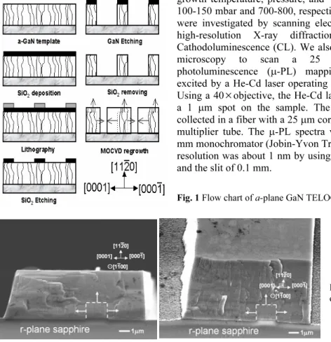
2 Experiments Figure 1 shows the flow chart of the process sequence of the a-GaN template and
subsequent TELOG. At first, the a-plane GaN templates with 1.5 µm thickness were grown with low
pressure metal-organic chemical vapor deposition (LP-MOCVD) on r-plane Al2O3 sapphire substrates
using conventional two-step growth technique. After a series of conventional photolithography
tech-niques, a 2-µm-seed / 18-µm-trench TELOG stripe pattern was applied parallel to the [1100]direction to
realize vertical c-plane sidewalls. Mask patterning was followed by etching of SiO2 using inductively
coupled plasma etching through the windows to the GaN epitaxial film. GaN stripes were etching
through the mask openings, down to the r-plane sapphire substrate, thus forming Ga-face [0001] and
N-face[0001]planes on the sidewalls and exposed r-plane sapphire at the bottom of the trenches by
reac-tive ion etching. To simplify the growth process, the SiO2 mask was removed by hydrofluoric acid and
followed by depositing a-plane GaN TELOG film using single-step growth process. In this study, the
growth temperature, pressure, and V/III ratio were 1190 oC,
100-150 mbar and 700-800, respectively. The grown samples were investigated by scanning electron microscopy (SEM), high-resolution X-ray diffraction and Cross-sectional Cathodoluminescence (CL). We also used a scanning optical
microscopy to scan a 25 µm
×
25 µmmicro-photoluminescence (µ-PL) mappings. The sample was
excited by a He-Cd laser operating on 325 nm with 25 mW.
Using a 40
×
objective, the He-Cd laser beam was focused toa 1 µm spot on the sample. The photoluminescence was
collected in a fiber with a 25 µm core and detected by a photo
multiplier tube. The µ-PL spectra were dispersed by a 320
mm monochromator (Jobin-Yvon Triax 320). The wavelength resolution was about 1 nm by using 300 grooves/mm grating and the slit of 0.1 mm.
Fig. 1 Flow chart of a-plane GaN TELOG process.
Fig. 2 Cross-sectional SEM of TELOG a-plane GaN.
102000 104000 106000 108000 100 1000 10000 || [0001] As grown FWHM=973 arcsec Int ens ity (c ou nt s) ω (arcsec) TELOG FWHM=816 arcsec 100000 102000 104000 106000 108000 100 1000 10000 As grown FWHM=1811 arcsec Int en si ty (c ou nt s) ω (arcsec) || [1-100] TELOG FWHM=352 arcsec (a) (b)
3 Results and discussion To observe the growth behaviour and mechanism, we stopped the process before the coalescence of the GaN films. The SEM images of cross-sectional and birds-view TELOG GaN by MOCVD were shown in Fig. 2. The growth rate of the Ga-face wing was twice faster than the N-face wing. However, the ratio of growth rate in Ga-face wing to N-face wing was not as high as an
order of magnitude reported by Imer et al. [8]. A thin GaN layer about 0.2 µm grown on the bottom of
the trenches, as shown in Fig. 2, could be the reason to hinder the lateral growth rate in the Ga-face wing and hence affect the epitaxial quality.
High-resolution X-ray rocking curves along [0001] c and [1100] m directions, as shown in Fig. 3,
revealed that the a-plane GaN templates suffer serious anisotropic structural characteristics. The FWHM
of X-ray rocking curves for an as-grown a-GaN 1.5 µm bulk layer in [1100] direction is almost twice as
large as that in [0001] direction. It shows that the strains between the orthogonal crystal axes, c-axis and
m-axis, are quite different and enhance the formation of line defects. Moreover, the surface geometry could show a wavy, stripe-like growth feature if the nucleation layer was not optimized or the epitaxial film was thick [2]. However, after lateral overgrowth, the stresses of TELOG layer were released in both
c-axis and m-axis and thus the crystal quality was enhanced especially in the [1100] direction. As shown
in Fig. 3, the FWHM of X-ray rocking curves for a TELOG layer was reduced from 1811 arcsec to 352 arcsec. Since the strip of the TELOG layer did not coalesce, we observed obvious wing tilt phenomenon along [0001] direction leading to the broadening effect of the X-ray rocking curve. Unlike the symmetric
wing tilt in c-plane ELOG GaN [9, 10] the wing tilt in a-plane TELOG GaN is asymmetric shown in the
X-ray rocking curve, resulting from the different lateral growth rates of the window GaN in the [0001]
and the [0001] directions [7]. Although the FWHM of X-ray rocking curves for a TELOG layer was
only reduced from 973 arcsec to 816 arcsec, the crystal quality would be better as the TELOG film fully coalesced to lessen wing tilt phenomenon.
Fig. 3 High-resolution X-ray rocking curves of as-grown and TELOG a-plane GaN (a) in [0001] direction (b) in [1 100] direction.
Figure 4 shows a µ-PL mapping of a-plane TELOG stripes. Five different regions can be
distin-guished in the TELOG sample and were labeled with numbers 1 to 5. Comparing the µ-PL mapping with
the SEM image, region 5 showing the lowest µ-PL intensity area can be identified as the un-coalesced
trenched region since a-GaN grown on r-sapphire without a nucleation layer showed a textured surface
with worst crystal quality. On the other hand, the region 1
show-ing the strongest µ-PL intensity area can be identified as the
N-face GaN wing. Region 2 is the stripped a-GaN seed. Regions 3
and 4 belong to the Ga-face GaN wing. Interestingly, region 3 standing at the initial region of the Ga-face GaN wing shows a higher PL intensity than that in region 4.
Fig. 4 µ-PL spectra and image of a-plane TELOG. 350 400 450 500 550 600 1000 2000 3000 4000 5000 6000 7000 8000 Wavelength(nm) In te ns ity (a .u .) 5 4321
The threading dislocation densities (TDD) of stripped GaN seed estimated by TEM, shown as Fig. 5
(a) in region 2 was more than 1×1010 cm−2. TDD of Ga-face GaN wing in region 4 was about 9×109 cm−2
and TDD of N-face GaN wing in region 1 was about 3×107 cm−2, three orders of magnitude lower than
planar films. The lower dislocation density in region 3 in comparison to the region 4 was in accordance with a higher PL intensity. Because the lateral growth mode could be affected when the laterally grown layers encounters the underlying GaN layers, we suggest that the crystal quality of Ga-face GaN with a
higher growth rate could be easily affected by the thin a-GaN layer grown on the bottom of the
un-coalesced windows. Due to the relatively low growth rate of the thin a-GaN layer on the bottom of the
trench, the crystal quality of the Ga-face GaN wing at the beginning of the lateral growth was good while
the thin a-GaN layer was not formed, resulting in a low
dislo-cation and high PL intensity area of region 3. As a result, to
obtain a better crystal quality a-plane TELOG GaN for the
most of the area, the trench depth shall be down to at least 0.2 µm deeper than the sapphire surface. To realize the relation-ship of optical property and TDD, the Cross-sectional
Ca-thodoluminescence (CL) image of a-plane TELOG was
pho-tographed, shown as Fig. 5(b). The CL intensity distribution is
almost the same as the results investigated by µ-PL and TEM.
So that the dislocations still perform as the strongly
non-radiative center in a-plane GaN film and become the principle
problem what should be solved immediately.
Fig. 5 (a) Cross-sectional TEM image and (b) cross-sectional CL image of a-plane GaN TELOG
4 Conclusions In conclusion, the quality of a-plane GaN film was successfully improved by using TELOG and the TDD can be reduced largely. Meanwhile the phenomenon of anisotropic in-plane strain between different crystal axis also can be mitigated by TELOG. Furthermore, the best quality area stands at the N-face GaN wing. The Ga-face GaN is easier to overgrowth and is influenced by the thin GaN
layer on the bottom of trench. According the results of µ-PL and CL, the threading dislocations are the
strongly non-radiative center in a-plane GaN film. Finally, we conclude that a narrower stripped GaN
seeds and deeper stripped patterns etched into the surface of sapphire can derive a better quality a-plane
TELOG GaN film.
Acknowledgements The authors would like to specially acknowledge the financial support by the Ministry of Economic Affairs, Taiwan, Republic of China. This work was supported by the MOE ATU program and in part by the National Science Council of Republic of China (ROC) in Taiwan under contract No.NSC 94-2120-M-009-007 and No. NSC 94-2215-E-009-082.
References
[1] P. Waltereit, O. Brandt, A. Trampert, H. T. Grahn, J. Menniger, M. Ramsteiner, M. Reiche, and K. H. Ploog, Nature (London) 406, 865 (2000).
[2] M. D. Craven, S. H. Lim, F. Wu, J. S. Speck, and S. P. DenBaars, Appl. Phys. Lett. 81, 469 (2002).
[3] M. D. Craven, A. Chakraborty, B. Imer, F. Wu, S. Keller, U. K. Mishra, J. S. Speck, and S. P. DenBaars, phys. stat. sol. (c) 1, 4 (2003).
[4] E. S. Hellman, Z. Liliental-Weber, and D. N. E. Buchanan, MRS Internet J. Nitride Semicond. Res. 2, 30 (1997).
[5] P. Waltereit, O. Brandt, M. Ramsteiner, A. Trampert, H. T. Grahn, J. Menniger, M. Reiche, R. Uecker, P. Reiche, and K. H. Ploog, phys. stat. sol. (a) 180, 133 (2000).
[6] H. Wang, C. Chen, Z. Gong, J. Zhang, M. Gaevski, M. Su, J. Yang, and M. A. Khan, Appl. Phys. Lett. 84. 499 (2004).
(a)
[7] M. D. Craven, S. H. Lim, F. Wu, J. S. Speck, and S. P. DenBaars, Appl. Phys. Lett. 81, 1201 (2002). [8] B. M. Imer, F. Wu, S. P. DenBaars, and J. S. Speck, Appl. Phys. Lett. 88, 061908 (2006).
[9] P. Fini, H. Marchand, J. P. Ibbetson, S. P. DenBaars, U. K. Mishra, and J. S. Speck, J. Cryst. Growth 209, 581 (2000).
[10] W. M. Chen, P. J. McNally, K. Jacobs, T. Tuomi, A. N. Danilewsky, Z. R. Zytkiewicz, D. Lowney, J. Kanatha-rana, L. Knuuttila, and J. Riikonen, J. Cryst. Growth 243, 94 (2002).
![Fig. 3 High-resolution X-ray rocking curves of as-grown and TELOG a-plane GaN (a) in [0001] direction (b) in [1 100] direction](https://thumb-ap.123doks.com/thumbv2/9libinfo/7670502.141306/3.892.140.710.599.783/high-resolution-rocking-curves-grown-telog-direction-direction.webp)

