A Low Quiescent Current Asynchronous Digital-LDO
With PLL-Modulated Fast-DVS Power Management
in 40 nm SoC for MIPS Performance Improvement
Yu-Huei Lee, Student Member, IEEE, Shen-Yu Peng, Chao-Chang Chiu, Student Member, IEEE,
Alex Chun-Hsien Wu, Ke-Horng Chen, Senior Member, IEEE, Ying-Hsi Lin, Shih-Wei Wang, Tsung-Yen Tsai,
Chen-Chih Huang, and Chao-Cheng Lee
Abstract—A low quiescent current asynchronous digital-LDO (D-digital-LDO) regulator integrated with a phase-locked loop (PLL)-modulated switching regulator (SWR) that achieves the near-optimum power management supply for core processor in system-on-chip (SoC). The parallel connection of the asyn-chronous D-LDO regulator and the ripple-based control SWR can accomplish fast-DVS (F-DVS) operation as well as high power conversion efficiency. The asynchronous D-LDO regulator controlled by bidirectional asynchronous wave pipeline realizes the F-DVS operation, which guarantees high million instructions per second (MIPS) performance of the core processor under distinct tasks. The use of a ripple-based control SWR operating with a leading phase amplifier ensures fast response and stable operation without the need for large equivalent-series-resistance, thus reducing the output voltage ripple for the enhancement of supply quality. The fabricated chip occupies 1.04 in 40 nm CMOS technology. Experimental results show that a 94% peak efficiency with a voltage tracking speed of 7.5 as well as the improved MIPS performance by 5.6 times was achieved.
Index Terms—Asynchronous digital-LDO regulator, bidirec-tional asynchronous wave pipeline, dynamic voltage scaling, hybrid operation, million instructions per second performance, power conversion efficiency, power module, ripple-based control, switching regulator.
I. INTRODUCTION
S
YSTEM-ON-A-CHIP (SoC) is the design trend in cur-rently available integrated circuits. Multiple operation functions, which are achieved by using both analog and digital circuits, can be combined into a single chip to minimize the Manuscript received August 27, 2012; revised October 19, 2012; accepted December 12, 2012. Date of publication January 21, 2013; date of current version March 22, 2013. This paper was approved by Guest Editor Hideyuki Kabuo. This work was supported by the National Science Council, Taiwan, under Grants NSC 101-2220-E-009-047, NSC 101-2220-E-009-052, and NSC 101-2622-E-009-004-CC2.Y.-H. Lee, S.-Y. Peng, C.-C. Chiu, and A. C.-H. Wu are with the Institute of Electrical Control Engineering, National Chiao Tung University, Hsinchu, Taiwan.
S.-W. Wang is with the Institute of Electrical Control Engineering, National Chiao Tung University, Hsinchu, Taiwan, and also with Realtek Semiconductor Corporation, Hsinchu, Taiwan.
K.-H. Chen is with the Institute of Electrical Control Engineering, National Chiao Tung University, Hsinchu 30010, Taiwan (e-mail: khchen@cn.nctu.edu. tw).
Y.-H. Lin, T.-Y. Tsai, C.-C. Huang, and C.-C. Lee are with Realtek Semicon-ductor Corporation, Hsinchu, Taiwan.
Color versions of one or more of the figures in this paper are available online at http://ieeexplore.ieee.org.
Digital Object Identifier 10.1109/JSSC.2013.2237991
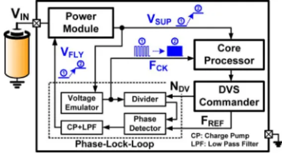
Fig. 1. Integrated power module with a PLL-modulated closed-loop operation for both DVS and DFS operations in SoC.
printed circuit board area as well as the total volume of portable devices. Power modules, which are demanded to provide high-quality supply voltages and to have high power conver-sion efficiency, are integrated to properly manage the supply voltages for sub-circuits, thus strengthening SoC performance [1]–[4]. As shown in Fig. 1, the system core processor is sup-plied by an integrated power module, which might be realized by using inductor-based switching regulators (SWRs) and/or low-dropout (LDO) regulators. To reduce power consumption and to improve core processor performance with distinct tasks, the function of a phase-locked loop (PLL) is implemented to adjust the supply voltage dynamically and to provide the appropriate operation frequencies as requested by the core processor [5]. Frequency is indicated by the dynamic voltage scaling (DVS) commander, which sends the signal
and the reference frequency to the PLL. The is rapidly changed to achieve the dynamic frequency scaling (DFS) operation so that the requirement of distinct tasks in the core processor would be met [6]–[8]. The DVS operation is activated by the indicative voltage which helps obtain a near-optimum voltage level [9]–[11]. Moreover, the PLL helps smoothly adjust the with a determined for the core processor to minimize the effect of process, voltage, and temperature (PVT) variations.
Million instructions per second (MIPS) is an appropriate in-dicator or evaluator for core processor performance [12], [13]. Operation frequency, which determines the execution speed of instructions, is the key factor in MIPS performance. Thus, DFS operation is utilized to meet the expected MIPS with distinct tasks in core processor. However, DVS operation should also be activated for the proper adjustment of supply voltage. The 0018-9200/$31.00 © 2013 IEEE
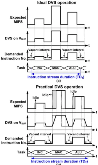
Fig. 2. MIPS illustration of different tasks in core processor under (a) ideal DVS operation and (b) practical DVS operation.
near-optimum supply voltage helps minimize the propagation delay to guarantee fast operation frequency in high MIPS con-ditions and reduce needless power loss to realize power-effi-cient operation in low MIPS conditions. As shown in Fig. 2(a), which illustrates an ideal DVS operation, supply voltage can be immediately changed to the different voltage levels. The number of demanded instructions varies according to the dis-tinct tasks executing in core processor. Vacant intervals are ob-served between each peak instructions, which can be considered the operated buffer stage. Satisfactory supply voltages ensure that the varying MIPS performances will correctly correspond to the demanded numbers of instructions. Therefore, the has to be rapidly adjusted to guarantee proper task operations.
The voltage tracking period is derived in practical DVS op-eration as shown in Fig. 2(b). The expected MIPS performance can be achieved by using adequate supply voltage . An idle stage, which is utilized to block the execution in core pro-cessor, is inserted until the reaches its target value in the voltage tracking period. The insertion of an idle stage prevents the operations with incorrect tasks but delays the instruction stream duration of sequential tacks. Thus, practical DVS opera-tion derives longer instrucopera-tion stream duraopera-tion, , compared
Fig. 3. Topologies of integrated power modules. (a) Simple SWR. (b) SWR in series with an A-LDO regulator. (c) SWR in parallel with an A-LDO regulator. (d) SWR in parallel with a D-LDO regulator.
with that of which is performed with the ideal DVS opera-tion. Voltage tracking speed on the has a significant effect on both the MIPS performance and the instruction stream dura-tion when core processor sequentially executes distinct tasks. As a result, the fast-DVS (F-DVS) operation needs to be achieved in an integrated power module to guarantee the performance of core processor as well as that of the SoC system.
Topologies of integrated power modules are shown in Fig. 3. Fig. 3(a)–(c) show the commonly used power modules. The SWR with a step-down function [14]–[16] shown in Fig. 3(a) has high power conversion efficiency but has limited voltage tracking speed due to its utilization of an inductor. The tracking speed is generally near tens of mV per micro-second, which is far from the demanded DVS performance in an integrated power module. Fig. 3(b) shows the power module achieved by the SWR with a cascaded analog-LDO (A-LDO) regulator [17]. The A-LDO regulator helps filter the switching noise from the SWR to generate a ripple-free output supply voltage for the noise-sensitive analog circuits in SoC. The A-LDO regulator has fast response because the bandwidth of LDO regulator is larger than that of the SWR. Nevertheless, the voltage tracking speed of this cascade structure is affected by the dropout voltage between and . If a large dropout voltage exists at the cascaded A-LDO regulator, a fast response is achieved at the ex-pense of efficiency. Trade-off exists between power efficiency and voltage tracking speed. The tracking speed of the cascade topology can reach up to hundreds of mV per micro-second, which is still below the demand of F-DVS operation. In ad-dition, the SWR can operate in parallel with an A-LDO regu-lator [18], [19] as illustrated in Fig. 3(c). The parallel combina-tion aims to realize hybrid operacombina-tion for both high efficiency and F-DVS operation. The SWR operates with an inductor-based structure to provide energy for high efficiency operation, whereas A-LDO regulator achieves fast voltage tracking be-cause of its large bandwidth. During the transient period, the A-LDO regulator can rapidly generate the supplementary rent for F-DVS operations. In steady-state, all the supply cur-rents are delivered by the SWR with a shutdown function to the A-LDO regulator to reduce power consumption. However, the
TABLE I
PERFORMANCECOMPARISONS OFPOWERMODULES
tracking speed is still limited by the bandwidth of the A-LDO regulator, which has a tracking rate of hundreds of mV per micro-second. This value is far from the expected rate of thou-sands of mV per micro-second.
To enhance the voltage tracking speed significantly, dig-ital-LDO (D-LDO) regulator is a suitable candidate for the integrated power module. Fig. 3(d) shows the hybrid operation achieved by the SWR in parallel with a D-LDO regulator [20]. Given that a D-LDO regulator has fast voltage tracking speed, the F-DVS operation is properly realized. The integrated power module proposed in this paper adopts this parallel structure to achieve both high efficiency and F-DVS operation. This pro-posed integrated power module contains a ripple-based control SWR and an asynchronous D-LDO regulator. Moreover, the asynchronous D-LDO regulator is controlled by the bidirec-tional asynchronous wave pipeline (BAWP), which can further improve tracking speed and can achieve a minimized static current consumption of 50 nA. Performance comparisons of these different integrated power modules are listed in Table I.
This paper is organized as follows. The PLL-modulated power module with an asynchronous D-LDO regulator and a ripple-based control SWR for hybrid operation is presented in Section II. An asynchronous D-LDO regulator structure with BAWP control is described in Section III. The ripple-based control SWR is illustrated in Section IV. Experimental results are shown in Section V. Finally, conclusions are made in Section VI.
II. PLL-MODULATED POWER MODULE WITH THEHYBRIDOPERATION
Structure of the proposed PLL-modulated power module is shown in Fig. 4. The PLL implementation helps activate the F-DVS operation to obtain a near-optimum voltage level at for the core processor [5]. The proposed power module achieves hybrid operation through a parallel connection of the ripple-based control SWR and the asynchronous D-LDO regulator. The PLL implementation generates the indicative voltage , which is the reference voltage for both SWR and D-LDO regulator.
The proposed SWR is operated with ripple-based control [21]–[24]. The output voltage is sent to the leading phase amplifier (LPA) to generate the sensing signal . The is then compared with the in terms of enabling the on-time generator to produce the control duty cycles for power switches, and . This comparator-controlled feedback methodology achieves a simple control structure which does not require a system compensation network. In addition, the
Fig. 4. Structure of the proposed PLL-modulated power module for the hybrid operation.
inductor-based SWR has the capability to provide a large supplying current and high efficiency despite its slow response. To achieve F-DVS operation for the core processor, the asyn-chronous D-LDO regulator is used for fast voltage tracking at the . The power switch arrays comprising P-MOSFETs and N-MOSFETs are implemented to achieve fast up-tracking and fast down-tracking, respectively. However, the fated power consumption and the unwilling output voltage ripple, which degrade the performance of the power module, stem from synchronous D-LDO regulators [25]–[28] that utilize a clock. In the proposed asynchronous D-LDO regulator, the BAWP controls the driving capability of power switches without the need of clock signals, and thereby minimizing current con-sumption considerably. A fast loop is exhibited in the proposed power module for the rapid regulation of the because the asynchronous D-LDO regulator can achieve F-DVS operation without the bandwidth limitation derived from conventional A-LDO regulators. Moreover, a freeze mode is also utilized in BAWP to stop the wave pipeline operation, such that the ultra-low current consumption of 50 nA can be obtained in the steady-state.
To guarantee the high efficiency operation of the proposed power module, the asynchronous D-LDO regulator must be shut down due to the existence of dropout voltages on power
Fig. 5. Hybrid operation. (a) F-DVS operation with distinct power request in core processor. (b) Load transient response with different load variations at the output.
switches. That is, the sensing current , which is propor-tional to the current of , helps the SWR take over the full current driving function in steady-state. , which can also be regard as the auxiliary current, is obtained through the current sensing implementation [29]. That is, once the power switches conduct the driving current for the , the can be carried out so as to increase the driving capability of the SWR. As a result, the driving current will be supplied by the SWR while the current flowing through the power switches in D-LDO regulator will be eliminated to get high efficiency. High power conversion efficiency and F-DVS operation can be simultaneously achieved in the integrated power module for SoC.
The proposed hybrid operations are illustrated in Fig. 5. The F-DVS operation is described in Fig. 5(a). With different requested power from the core processor, the indicative voltage can be modulated to distinct voltage levels for the activation of F-DVS operation at the . The asynchronous D-LDO regulator can provide the supplementary current to help rapidly adjust the output voltage level of for F-DVS operation. In addition, when the reaches its target value, the current can be set to zero to ensure high efficiency operation. The load transient response depicted in Fig. 5(b) has a response similar to that of the proposed hybrid operation. When the increases to provide a
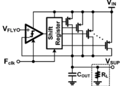
Fig. 6. Structure of synchronous D-LDO regulator.
Fig. 7. Illustration of the synchronous D-LDO regulator operation.
large amount of power to the core processor, the helps minimize the voltage variation at the and also ensures high power conversion efficiency in steady-state. Therefore, the hybrid operation simultaneously guarantees smooth supply voltage and high power conversion efficiency operation at both F-DVS operation and load transient response.
III. ASYNCHRONOUSDIGITAL-LDO REGULATOR A D-LDO regulator is the characteristic of fast transient re-sponse by increasing operation frequency. With the implemen-tation of a power switch array, the dropout voltage is rapidly ad-justed through the digital control circuit. D-LDO is suitable for operation with low supply voltage because no analog circuit is presented in its control loop. In addition, the system bandwidth limitation, which is derived from the A-LDO regulator struc-ture, is effectively released. Therefore, fast transient response can be guaranteed with the utilization of a D-LDO regulator.
A. Synchronous D-LDO Regulator
A Conventional D-LDO regulator usually adopts the syn-chronous control scheme [25]–[28] as shown in Fig. 6, where a clock signal is utilized to realize the operation. The comparator is used to monitor the output voltage with the reference voltage . In this work, a shift register is employed to acti-vate the power switches. When large output power is requested to the D-LDO regulator, the comparator would detect the oc-currence of insufficient energy at the so that more power switches are turned on to provide the supplementary current. On the other hand, the power switches would be turned off if the exceeds the .
Synchronous D-LDO regulator performance is significantly affected by the operation clock frequency, . Given that the comparator has nearly infinite bandwidth, the shift register
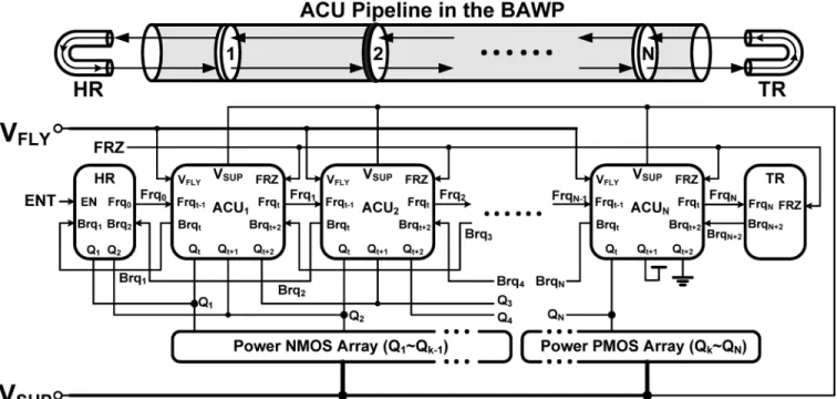
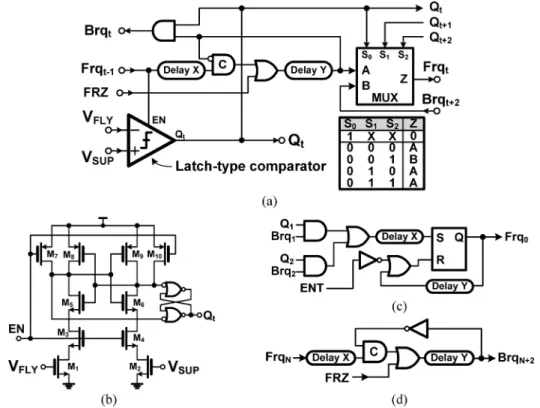
Fig. 8. Implementation of asynchronous D-LDO regulator with the bidirectional asynchronous wave pipeline (BAWP).
can be immediately informed to either increase or decrease the driving capability of power switches when the output loading is changed. However, the transient speed is mainly determined by because the shift register allows only one power switch to be turned on or off within per clock cycle in the synchronous D-LDO regulator. Illustration of the synchronous D-LDO regulator operation is shown in Fig. 7. If the synchronous D-LDO regulator operates with a slow frequency clock , small power consumption realizes the better current efficiency , compared with that of , which is derived with the fast frequency clock , thus resulting in larger current dissipation. However, fast tracking speed can be achieved by adopting the high frequency clock in a synchronous D-LDO regulator but results in the worse current efficiency compared with that when operating with a slow frequency clock . That is, higher frequency of leads to faster voltage tracking speed at the . Moreover, the current efficiency of the D-LDO regulator is inversely proportional to the frequency of . Fast voltage tracking speed can be ensured; however, current efficiency will be deteriorated in the synchronous D-LDO regulator with a high frequency clock. A trade-off between voltage tracking speed and current efficiency exists in the clock-triggered synchronous D-LDO regulator design.
B. Bidirectional Asynchronous Wave Pipeline (BAWP) Controlled Asynchronous D-LDO Regulator
The proposed BAWP controlled asynchronous D-LDO reg-ulator depicted in Fig. 4 achieves the F-DVS operation with the minimized current consumption. Fig. 8 shows the imple-mentation of BAWP controlled asynchronous D-LDO regulator. Operation of the BAWP is similar to a clock-free shift register for determining the activation of power switches. That is, no constant clock signal triggers the asynchronous control units
(ACUs) in BAWP. There are 32 ACU stages in this current de-sign. The signal ENT will be enabled by the processor in SoC when the hybrid operation is activated. The D-LDO regulator with ACUs can then operate to provide the supplementary en-ergy in order to obtain the requested power. With the activa-tion of the enabling signal ENT, the ACUs control the power switches to modulate the output voltage in the D-LDO regulator. As the result of asynchronous control scheme, only one ACU is activated at one time to minimize power dissipation. If the is smaller than the , the ACU pipeline exe-cutes the shift-right operation to turn on more power switches for regulation. Contrarily, the shift-left operation occurs when the is larger than the to decrease the energy delivered to the . In addition, the heading reflector (HR) and the terminal reflector (TR) are utilized as boundaries of BAWP owing to the removal of constant clock in asynchronous control. Unlike synchronous control, which requires a clock signal to activate all the control stages simultaneously, asyn-chronous control realizes the hand-shaking operation so that the problem of clock skew never occurs. The BAWP ensures that the ACU can be triggered by itself according to the energy de-mand of . Moreover, the freeze mode can be enabled by signal FRZ, so as to freeze the convergent stage of ACUs. There-fore, the output voltage ripple in the proposed asynchronous D-LDO regulator can be eliminated, and the current consump-tion can be further minimized.
Implementations of ACU, latch-type comparator, HR, and TR are shown in Fig. 9. Each ACU in Fig. 9(a) contains a latch-type comparator, a multiplexer, and the control logics to control one power switch for the modulation. The com-parator is enabled by its prior ACU stage. That is, the ACU is motionless until the requested signal, , is sent from its prior stage. The comparator compares the with the ref-erence voltage and generates the signal to control
Fig. 9. Implementations of (a) ACU, (b) latch-type comparator, (c) heading reflector (HR), and (d) terminal reflector (TR).
the corresponding power switch. The multiplexer determines the forward request signal from either the prior stage of or the later stage according to the control sig-nals to . The operation principle of ACU in the BAWP is shown in the table attached in Fig. 9(a). The latch-type com-parator is shown in Fig. 9(b). With the activation of enabling signal EN that is sent from the prior ACU stage, the output decides on state of corresponding power switch as well as on the forward request signal . Both HR and TR, as respec-tively shown in Fig. 9(c) and (d), help guarantee the request signal in the asynchronous BAWP at the first and last ACU stages, respectively. If the utilization of HR is missing, the re-quest signal underflows in the BAWP when the derives an overcharge at the first ACU stage. Similarly, TR helps pre-vent the request signal from overflowing in the BAWP while the
has insufficient energy at the last ACU stage.
Fig. 10(a) and (b) show the timing diagram of the single ACU operation at different conditions. If the is smaller than the in an ACU stage activated by signal , the control signal is pulled low to turn on the p-type power switch or to turn off the n-type power switch in the proposed asynchronous D-LDO regulator. Thus, the energy supply for the can be increased to raise the . The forward request signal is also set after a determined delay period, Delay , to facilitate the shift-right operation in the BAWP to increase load driving. On the other hand, the back request signal will be triggered if the is larger than the , so as to realize the shift-left operation in the BAWP to decrease the driving capability. Moreover, the periods, Delay and Delay , are utilized to guarantee correct logic functions in ACUs.
Fig. 10(c) shows the BAWP control for F-DVS operation. The needs to be raised to track the reference voltage
. Once the F-DVS operation is requested, the core cessor sends a de-freeze signal, such that the operation of pro-posed asynchronous D-LDO regulator can be changed from the freeze mode to the tracking mode. In this work, the BAWP be-haves the shift-right operation with the forward request signals, , , , and so on. When the reaches its target value of , the back request signals are issued to stop the delivery of supplementary energy to the . When the BAWP operation is converged to the two nearby ACU stages, the signal FRZ will be set by the processor to change the op-eration from the tracking mode back to the freeze mode. The F-DVS operation is ended through the indication of signal FRZ. Moreover, since all the ACUs are disabled in freeze mode, the current consumption of the proposed asynchronous D-LDO reg-ulator only requires approximately 50 nA, which is nearly equal to the leakage current derived by 40 nm core devices. As a re-sult, fast response and ultra-low static current consumption are simultaneously achieved by using the proposed asynchronous D-LDO regulator.
IV. RIPPLE-BASEDCONTROLSWR
To quickly take over the power supplying authority from the asynchronous D-LDO regulator at the end of hybrid operation for high efficiency, the SWR also needs to behave the advan-tage of fast response. Transient speed of SWR is theoretically restricted because the inductor current level cannot be instan-taneously raised within a finite charging period of time. Fur-thermore, system compensation limits the bandwidth, and thus worsens the transient response although it can guarantee the stable operation in pulse width modulation (PWM) control. Sev-eral fast transient techniques have been reported to enhance
Fig. 10. Timing diagrams. (a) Single ACU operation when the is smaller than the . (b) Single ACU operation when the is larger than the . (c) BAWP operation when the F-DVS is activated.
the transient response of SWR [30]–[32]; however, the com-plex circuit implementations would be unacceptable. Utiliza-tion of a ripple-based control in SWR is characterized by fast response because its reduced-complexity structure achieved by the comparator-controlled feedback scheme realizes a near-infi-nite system bandwidth in control loop. That is, the power stage immediately extends the inductor charging or discharging pe-riods for the rapid modulation of inductor current when the de-mand for supply power is changed.
A. Operation of Ripple-Based Control SWR
Circuit structure of the proposed ripple-based control SWR is shown in Fig. 4. Conventional ripple-based control design uses a large equivalent-series-resistance (ESR) on output capacitor to ensure stable operation [21]–[24]. Stability criterion of the ripple-based control step-down converter is given in [21] and is shown in (1).
(1) where represents the ESR value on output capacitor . is the period that the high-side power MOSFET of buck converter is turned on. Utilization of a large ESR causes the large output voltage ripple, and thus deteriorating the quality of supply voltage for the core processor. To strengthen the supply quality of SWR with a ripple-based control, ESR on the output capacitor has to be as small as possible. The LPA shown in Fig. 4 is used to guarantee stable operation when a small ESR is adopted in the ripple-based control SWR, so
Fig. 11. Operations of the ripple-based control SWR with LPA circuit.
as to achieve low output voltage ripple. The operations of the ripple-based control SWR with LPA are described in Fig. 11.
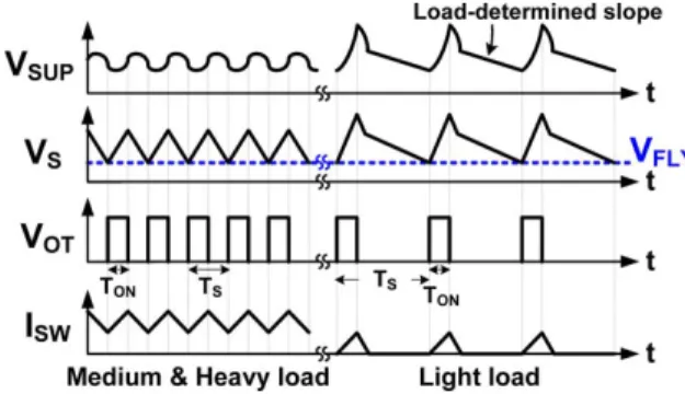
An LPA circuit serves as the differentiator that generates a sensing signal, , which is proportional to the differentiation of voltage ripple on and is similar to the current ripple of the inductor in SWR. In case of medium or heavy load conditions, the continuous-conduction-mode (CCM) operation is activated to provide high driving capability. When the touches the ref-erence voltage , the on-time generator shown in Fig. 4 is activated to generate a constant on-time pulse, , with the on-time period, , so that the high-side power MOSFET can be turned on to activate the inductor charging period. On the other hand, the low-side power MOSFET is turned on to release the energy from the inductor at the end of the on-time period. Nevertheless, the electromagnetic interference (EMI) problem becomes a tough issue when the ripple-based control SWR is integrated in SoC. Since no constant frequency clock
Fig. 12. Schematic of the on-time generator.
exists in ripple-based control, the varied switching frequency, which results in a noisy frequency spectrum, affects the func-tions of other integrated circuits in SoC. In other words, if the switching frequency is nearly constant in CCM operation, the EMI problem will be alleviated by an external EMI filter.
Duty cycle of the ripple-based control buck converter can be expressed by (2).
(2) where is the switching period. Thus, the switching frequency of SWR, , can be described in (3).
(3) where will be a constant value if only the is proportional and inversely proportional to and , respectively. That is, the adjustment of with the distinct input and output voltages results in a nearly constant switching frequency in the ripple-based control SWR.
The ripple-based control SWR can also operate with a re-duced switching frequency at light loads as shown in Fig. 11. Unlike the PWM control that operates with a constant frequency clock to trigger the switching cycle, the ripple-based control re-duces the switching frequency at light loads to minimize power loss and obtain high efficiency. The discontinuous-conduction-mode (DCM) operation is automatically achieved by using the comparator-triggered on-time generator and the zero current de-tection mechanism at the low-side power MOSFET [33], [34]. As a result, the switching frequency in DCM operation varies according to the load-determined slope at caused by dis-tinct output load conditions, such that the power conversion ef-ficiency can be guaranteed at the light load conditions.
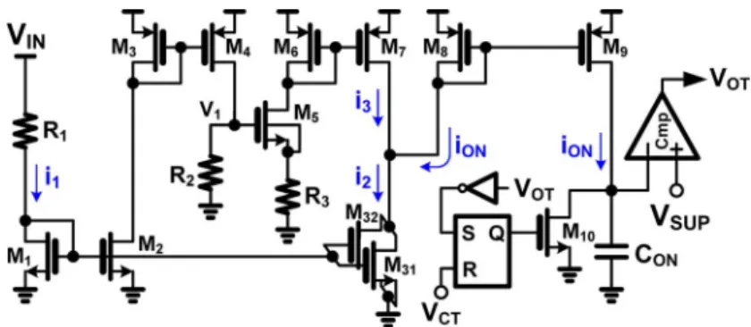
B. On-Time Generator
Fig. 12 shows the circuit of on-time generator. The on-time period, , of the on-time signal, , is determined by both and . The current is generated by as shown in (4) that the large will indicate the large .
(4) To enhance the linearity of voltage-to-current conversion of (4), the , which is the non-ideal factor caused by the gate-to-source voltage of , needs to be eliminated. The MOSFET
also forms another voltage-to-current conversion to gen-erate the current described in (5), which is also affected by the gate-to-source voltage . By removing the body ef-fect on , both the process-dependent gate-to-source voltages, and , become nearly equivalent only if and are implemented with the same aspect ratio.
(5) As a result, the , which denotes duration that voltage crossed on the capacitor is charged to the by the current , can be obtained as shown in (6). Finally, once the resistors, , , and , are chosen properly, the shown in (7) becomes proportional and inversely proportional to the output voltage and to the input voltage , respectively. This condition helps achieve a nearly constant switching frequency in the ripple-based control SWR.
(6) (7)
C. Leading Phase Amplifier (LPA)
Fig. 13 shows the proposed LPA circuit, which is used to guarantee the stable operation of the ripple-based control SWR without the use of a large ESR. Fig. 13(a) depicts the circuit schematic. A negative feedback loop formed by the trans-mits the voltage ripple at the into the LPA. A voltage-con-trol-current-source (VCCS) structure is implemented by using , , , and the capacitor to achieve the phase lead operation. The structure can also be regarded as the high-pass filter that enables the ripple voltage of to be converted to the current through the . The voltage ripple at the of the buck converter is illustrated in (8).
Fig. 13. LPA circuit in the proposed SWR. (a) Schematic. (b) Frequency response.
where the is the inductor current ripple.
The VCCS circuit acts as the differentiator. Thus, the is generated through the shown in (9) with the s-domain description.
(9) The can be seemed as the small signal current which is mir-rored to for generating the sensing signal . Therefore, the , which can be regarded as the differential result of , is then obtained by means of the output resistance as shown in (10).
(10) Here, the can be further simplified as expressed in (11) if a small is used.
(11) Consequently, the ac signal on replicates the inductor cur-rent ripple . That is to say, the inductor current ripple in-formation is obtained without the need for a large ESR through the proposed LPA. Moreover, the DC level adjusting is used to accomplish the dc voltage tracking between the and the . A compensated feedback loop achieved by the ensures the to track the dc voltage value of . Therefore, the can be regulated to its target value because of the com-parator-controlled structure in the ripple-based control SWR.
Frequency response of the proposed LPA circuit is shown in Fig. 13(b). A low-frequency zero, which is generated by the
Fig. 14. Simulated result of the LPA circuit in ripple-based control SWR.
Fig. 15. Measured waveform of F-DVS operation with both up-tracking and down-tracking operations.
capacitor , ensures the phase lead operation as well as the differentiate function. By adopting the differentiate func-tion, the becomes proportional to the inductor current ripple without adopting a large ESR on the output capacitor. Thus, output voltage ripple in the ripple-based control SWR can be surely minimized. In the meanwhile, stability can also be guar-anteed as well as high power conversion efficiency and fast re-sponse in ripple-based control SWR. Fig. 14 shows the simu-lated result that demonstrates the utilization of LPA circuit in the ripple-based control SWR.
V. EXPERIMENTALRESULTS
The proposed integrated power module with asynchronous D-LDO regulator and SWR for hybrid operation was fabricated by 40 nm CMOS technology. Nominal output voltage of the pro-posed power module is 1 V. Off-chip inductor is 1 with the output capacitor of 0.1 in SWR. Measure F-DVS operation is shown in Fig. 15. If is requested with a 0.18 V voltage step with the of 3.3 V, the asynchronous D-LDO regu-lator helps guarantee the F-DVS operation within 20 ns. When the up-tracking is enabled with hybrid operation, the BAWP in asynchronous D-LDO regulator activates the shift-right opera-tion to turn on the p-type power switches to increase the supple-mentary current. Therefore, the tracking speed can be achieved about 9 . The freeze mode also helps eliminate the output voltage ripple to derive the high-quality supply. Compared the hybrid operation to that of SWR regulator only, the voltage tracking speed in SWR is obviously restricted due to the de-termined system bandwidth and the inductor.
Besides, the SWR will provide all load current to shut down the asynchronous D-LDO regulator for achieving high power
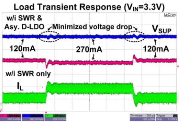
Fig. 16. Measure load transient response with and without the hybrid operation.
Fig. 17. Measure F-DVS operation with distinct power modules.
conversion efficiency. The similar operation is derived in the down-tracking operation. The BAWP in asynchronous D-LDO regulator can operate with the shift-right operation to fast mod-ulate the , so that the improved voltage tracking operation is obtained. Fig. 16 shows the load transient response with the of 3.3 V. The hybrid operation can also be activated that the asynchronous D-LDO regulator will rapidly provide the com-pensated current if the demanded supply current is increased. Thus, the voltage drop at the can be minimized when the hybrid operation is activated.
Fig. 17 shows the measured F-DVS operation with dis-tinct power modules with the of 3.3 V. Voltage tracking speed can be improved to thousands of mV per micro-second due to the utilization of asynchronous D-LDO regulator. The BAWP ensures fast response for voltage tracking and achieves power-efficient operation by using asynchronous control scheme. A-LDO performance is limited by the finite bandwidth. The tracking speed in SWR is restricted by both bandwidth and inductor. Here, fast response of the proposed asynchronous D-LDO regulator is demonstrated. Fig. 18 shows the power conversion efficiency. Since the measured efficiency is obtained in steady-state, the hybrid operation in the pro-posed power management was ended so that the propro-posed asynchronous D-LDO regulator can be operated with freeze mode in steady-state. If the operation contains the auxiliary current , all driving current will be supplied by the SWR and the asynchronous D-LDO regulator remains only a 50 nA current consumption in steady-state to get high efficiency. That is, the SWR only operation helps obtain the peak efficiency of 94%. Once the hybrid operation is activated without the auxiliary current , the asynchronous D-LDO regulator will not be shut down in steady-state. Therefore, efficiency of the
Fig. 18. Measure steady-state power conversion efficiency.
Fig. 19. Measured MIPS performance in core processor with distinct power modules.
Fig. 20. Chip micrograph.
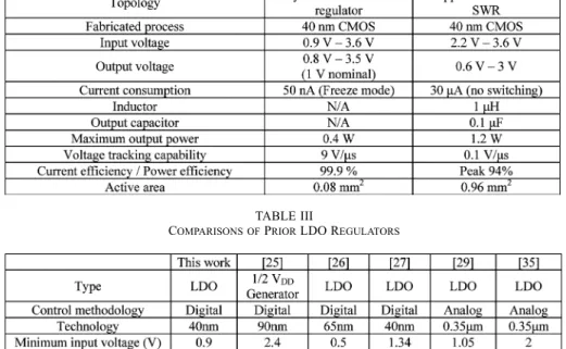
proposed power management will be deteriorated since partial of the load current is provided by the D-LDO regulator. Fig. 19 shows the improvement of MIPS performance in the realistic core processor. It demonstrates the MIPS can be improved by 5.6 times with the proposed F-DVS operation compared to that of the SWR only. Since the asynchronous D-LDO regulator can help rapidly modulate the supply voltage, the idle period in the practical DVS operation can be minimized. This improvement helps the MIPS performance in the core processor match up with the design target, so as to shorten the total instruction steam duration with the serious tasks for guarantee the operated efficiency in core processor. Fig. 20 shows the chip micrograph with 1.04 active area. The test chip integrates both SWR and asynchronous D-LDO regulator to achieve the hybrid op-eration. The detailed design specifications are listed in Table II, while the comparisons of the prior LDO designs are shown in Table III. Despite of fast response in the proposed asynchronous
TABLE II
DESIGNSPECIFICATIONS OFPROPOSEDPOWERMODULE
TABLE III
COMPARISONS OFPRIORLDO REGULATORS
D-LDO regulator, the minimized 50 nA current consumption also helps achieve the current efficiency of 99.97%.
VI. CONCLUSION
A power module of the asynchronous D-LDO regulator and the ripple-based control SWR is proposed to achieve the inte-gration in SoC. PLL-modulate control loop provides the indica-tive reference voltage to guarantee the near-optimum supply voltage according to the demand from system core processor. Parallel connection of both D-LDO regulator and SWR forms the hybrid operation to realize F-DVS operation and high power conversion efficiency. The asynchronous D-LDO regulator en-sures the F-DVS operation with the clock-free BAWP control, which can further minimize the current consumption to 50 nA by freeze mode operation, for power saving. The ripple-based control SWR operates with the simple structure while accom-plishing the fast response. Utilization of the LPA helps guar-antee the stale operation with the need of large ESR, so as to strengthen the supply quality. The proposed power module fab-ricated by 40 nm CMOS process occupies a 1.04 sil-icon area, which achieves 94% peak efficiency with the voltage tracking speed of 7.5 for the 5.6 times MIPS performance improvement.
REFERENCES
[1] G. Patounakis, Y. W. Li, and K. L. Shepard, “A fully integrated on-chip DC-DC conversion and power management system,” IEEE J. Solid-State Circuits, vol. 39, no. 3, pp. 443–451, Mar. 2004.
[2] I. Doms, P. Merken, C. V. Hoof, and R. P. Mertens, “Capacitive power management circuit for micropower thermoelectric generators with a 1.4 controller,” IEEE J. Solid-State Circuits, vol. 44, no. 10, pp. 2824–2833, Oct. 2009.
[3] Y.-H. Lee, Y.-Y. Yang, K.-H. Chen, Y.-H. Lin, S.-J. Wang, K.-L. Zheng, P.-F. Chen, C.-Y. Hsieh, Y.-Z. Ke, Y.-K. Chen, and C.-C. Huang, “A DVS embedded power management for high efficiency integrated SoC in UWB system,” IEEE J. Solid-State Circuits, vol. 45, no. 11, pp. 2227–2238, Nov. 2010.
[4] J. Shi, E. Soenen, A. S. Roth, Y.-C. Hsu, and M. Kinyua, “Practical considerations for a digital inductive-switching DC/DC converter with direct battery connect in deep sub-micron CMOS,” IEEE J. Solid-State Circuits, vol. 47, no. 8, pp. 1946–1959, Aug. 2012.
[5] Y.-H. Lee, C.-C. Chiu, S.-Y. Peng, K.-H. Chen, Y.-H. Lin, C.-C. Lee, C.-C. Huang, and T.-Y. Tsai, “A near-optimum dynamic voltage scaling (DVS) in 65 nm energy-efficient power management with frequency-based control (FBC) for SoC system,” IEEE J. Solid-State Circuits, vol. 47, no. 11, Nov. 2012, to be published.
[6] J.-H. Kim, Y.-H. Kwak, M. Kim, S.-W. Kim, and C. Kim, “A 120-MHz–1.8-GHz CMOS DLL-based clock generator for dynamic frequency scaling,” IEEE J. Solid-State Circuits, vol. 41, no. 9, pp. 2077–2082, Sep. 2006.
[7] K. J. Nowka, G. D. Carpenter, E. W. MacDonald, H. C. Ngo, B. C. Brock, K. I. Ishii, T. Y. Nguyen, and J. L. Burns, “A 32-bit PowerPC system-on-a-chip with support for dynamic voltage scaling and dy-namic frequency scaling,” IEEE J. Solid-State Circuits, vol. 37, no. 11, pp. 1441–1447, Nov. 2002.
[8] M. Onouchi, Y. Kanno, M. Saen, S. Komatsu, Y. Yasu, and K. Ishibashi, “A low-power wide-range clock synchronizer with pre-dictive-delay-adjustment scheme for continuous voltage scaling in DVFS,” IEEE J. Solid-State Circuits, vol. 45, no. 11, pp. 2312–2320, Nov. 2010.
[9] T. D. Burd, T. A. Pering, A. J. Stratakos, and R. W. Brodersen, “A dynamic voltage scaled microprocessor system,” IEEE J. Solid-State Circuits, vol. 35, no. 11, pp. 1571–1580, Nov. 2000.
[10] B. H. Calhoun and A. P. Chandrakasan, “Ultra-dynamic voltage scaling (UDVS) using sub-threshold operation and local voltage dithering,” IEEE J. Solid-State Circuits, vol. 41, no. 1, pp. 238–245, Jan. 2006.
R. Rogenmoser, D. Suh, E. Supnet, V. R. von Kaenel, and G. Yiu, “A 2 load/store pipe for a low-power 1-GHz embedded processor,” IEEE J. Solid-State Circuits, vol. 38, no. 11, pp. 1857–1865, Nov. 2003. [14] J. Xiao, A. V. Peterchev, J. Zhang, and S. R. Sanders, “A 4-
quies-cent-current dual-mode digitally controlled buck converter IC for cel-lular phone applications,” IEEE J. Solid-State Circuits, vol. 39, no. 12, pp. 2342–2348, Dec. 2004.
[15] H.-W. Huang, K.-H. Chen, and S.-Y. Kuo, “Dithering skip modulation, width and dead time controllers in highly efficient DC-DC converters for system-on-chip applications,” IEEE J. Solid-State Circuits, vol. 42, no. 11, pp. 2451–2465, Nov. 2007.
[16] K.-H. Chen, C.-J. Chang, and T.-H. Liu, “Bidirectional current-mode capacitor multipliers for on-chip compensation,” IEEE Trans. Power Electron., vol. 23, no. 1, pp. 180–188, Jan. 2008.
[17] K. Lee, F. C. Lee, J. Wei, and M. Xu, “Analysis and design of adaptive bus voltage positioning system for two-stage voltage regulators,” IEEE Trans. Power Electron., vol. 24, no. 12, pp. 2735–2745, Dec. 2009. [18] A. Barrado, R. Vázquez, E. Olías, A. Lázaro, and J. Pleite, “Theoretical
study and implementation of a fast transient response hybrid power supply,” IEEE Trans. Power Electron., vol. 19, no. 4, pp. 1003–1009, Jul. 2004.
[19] T.-W. Kwak, M.-C. Lee, and G.-H. Cho, “A 2 W CMOS hybrid switching amplitude modulator for EDGE polar transmitters,” IEEE J. Solid-State Circuits, vol. 42, no. 12, pp. 2666–2676, Dec. 2007. [20] Y.-H. Lee, S.-Y. Peng, C.-H. Wu, C.-C. Chiu, Y.-Y. Yang, M.-H.
Huang, K.-H. Chen, Y.-H. Lin, S.-W. Wang, C.-Y. Yeh, C.-C. Huang, and C.-C. Lee, “A 50 nA quiescent current asynchronous digital-LDO with PLL-modulated fast-DVS power management in 40 nm CMOS for 5.6 times MIPS performance,” in Proc. IEEE Symp. VLSI Circuits, Jun. 2012, pp. 178–179.
[21] R. Redl and J. Sun, “Ripple-based control of switching regulators — An overview,” IEEE Trans. Power Electron., vol. 24, no. 12, pp. 2669–2680, Dec. 2009.
[22] J. Sun, “Characterization and performance comparison of ripple-based control for voltage regulator modules,” IEEE Trans. Power Electron., vol. 21, no. 2, pp. 346–353, Mar. 2006.
[23] B. Sahu and G. A. Rincón-Mora, “An accurate, low-voltage, CMOS switching power supply with adaptive on-time pulse-frequency modu-lation (PFM) control,” IEEE Trans. Circuits Syst. I, Reg. Papers, vol. 54, no. 2, pp. 312–321, Feb. 2007.
[24] Y.-C. Lin, C.-J. Chen, D. Chen, and B. Wang, “A ripple-based constant on-time control with virtual inductor current and offset cancellation for DC power converters,” IEEE Trans. Power Electron., vol. 27, no. 10, pp. 4301–4310, Oct. 2012.
[25] P. Hazucha, S. T. Moon, G. Schrom, F. Paillet, D. Gardner, S. Ra-japandian, and T. Karnik, “High voltage tolerant linear regulator with fast digital control for biasing of integrated DC-DC converters,” IEEE J. Solid-State Circuits, vol. 42, no. 1, pp. 66–73, Jan. 2007.
[26] Y. Okuma, K. Ishida, Y. Ryu, X. Zhang, P.-H. Chen, K. Watanabe, M. Takamiya, and T. Sakurai, “0.5-V input digital LDO with 98.7% current efficiency and 2.7- quiescent current in 65 nm CMOS,” in Proc. IEEE Custom Integrated Circuits Conf. (CICC), Sep. 2010, pp. 1–4.
[27] M. Onouchi, K. Otsuga, Y. Igarashi, T. Ikeya, S. Morita, K. Ishibashi, and K. Yanagisawa, “A 1.39-V input fast-transient-response digital LDO composed of low-voltage MOS transistors in 40-nm CMOS process,” in Proc. IEEE Asian Solid-State Circuits Conf., Nov. 2011, pp. 37–40.
[28] K. Hirairi, Y. Okuma, H. Fuketa, T. Yasufuku, M. Takamiya, M. No-mura, H. Shinohara, and T. Sakurai, “13% power reduction in 16 b integer unit in 40 nm CMOS by adaptive power supply voltage control with parity-based error prediction and detection (PEPD) and fully in-tegrated digital LDO,” in IEEE Int. Solid-State Circuits Conf. (ISSCC) Dig. Tech. Papers, Feb. 2012, pp. 486–487.
[29] Y.-H. Lam and W.-H. Ki, “A 0.9 V 0.35 adaptively biased CMOS LDO regulator with fast transient response,” in IEEE Int. Solid-State Circuits Conf. (ISSCC) Dig. Tech. Papers, Feb. 2008, pp. 442–443.
Electron., vol. 24, no. 12, pp. 2692–2703, Dec. 2009.
[33] F.-F. Ma, W.-Z. Chen, and J.-C. Wu, “A monolithic current-mode buck converter with advanced control and protection circuits,” IEEE Trans. Power Electron., vol. 22, no. 5, pp. 1836–1846, Sep. 2007.
[34] E. J. Carlson, K. Strunz, and B. P. Otis, “A 20 mV input boost converter with efficient digital control for thermoelectric energy harvesting,” IEEE J. Solid-State Circuits, vol. 45, no. 4, pp. 741–750, Apr. 2010.
[35] M. Al-Shyoukh, H. Lee, and R. Perez, “A transient-enhanced low-qui-escent current low-dropout regulator with buffer impedance attenua-tion,” IEEE J. Solid-State Circuits, vol. 42, no. 8, pp. 1732–1742, Aug. 2007.
Yu-Huei Lee (S’09) was born in Taipei, Taiwan.
He received the B.S. and M.S. degrees from the Department of Electrical and Control Engineering, National Chiao Tung University, Hsinchu, Taiwan, in 2007 and 2009, respectively, and the Ph.D. degree from the Institute of Electrical Control Engineering, National Chiao Tung University, Hsinchu, Taiwan, in 2012.
He is a member of the Mixed Signal and Power IC Laboratory, Institute of Electrical Control Engi-neering, National Chiao Tung University, Hsinchu, Taiwan. His current research interests include the power management in-tegrated circuit design, light-emitting diode driver IC design, and analog integrated circuits.
Shen-Yu Peng was born in Hsinchu, Taiwan. He
received the B.S. degree from the Department of Electrical and Electronic Engineering, National Taiwan University of Science and Technology, Taipei, Taiwan, in 1997, and the M.S. degree in Electrical Engineering from the National Tsing Hua University, Hsinchu, Taiwan, in 1999. He is currently working toward the Ph.D. degree at the Institute of Electrical Control Engineering, National Chiao Tung University, Hsinchu, Taiwan.
From 1999 to 2012, he was a senior engineer at Sunplus and Tritan Technology Ltd, ROC, where he developed various dig-ital signal processors, digdig-itally class-D amplifiers and audio/image signal pro-cessing algorithms. His current research interests are in the area of SoC power management and Class-D amplifier design.
Chao-Chang Chiu (S’12) received the B.S. degree
from Fu Jen Catholic University, Taipei, Taiwan, in 2008, and the M.S. degree from National Central University, Taoyuan, Taiwan, in 2010, at the De-partment of Electrical Engineering. He is currently working toward the Ph.D. degree at the Institute of Electrical Control Engineering, National Chiao Tung University (NCTU), Hsinchu, Taiwan.
He is a member of the Mixed-Signal and Power Management Integrated Circuit Laboratory, Institute of Electrical Control Engineering, NCTU. His cur-rent research interests include the power management integrated circuit designs and analog integrated circuit designs.
Alex Chun-Hsien Wu was born in New Taipei City,
Taiwan. He received the B.S. degree in electrical engineering from National Taiwan University of Science and Technology, Taipei, Taiwan, in 2007, and the M.S. degree in electronic engineering from National Tsing Hua University, Hsinchu, Taiwan, in 2010. He is currently pursuing the Ph.D. degree in electrical and control engineering from National Chiao Tung University, Hsinchu, Taiwan.
His main research area during his M.S. career is microelectronic and mechanical systems (MEMS), which include bio-MEMS and micro-sensor design. His current research includes the power management integrated circuit design and Mixed-signal ICs design.
Ke-Horng Chen (M’04–SM’09) received the B.S.,
M.S., and Ph.D. degrees in electrical engineering from National Taiwan University, Taipei, Taiwan, in 1994, 1996, and 2003, respectively.
From 1996 to 1998, he was a part-time IC De-signer at Philips, Taipei, Taiwan. From 1998 to 2000, he was an Application Engineer at Avanti, Ltd., Taiwan. From 2000 to 2003, he was a Project Manager at ACARD, Ltd., where he was engaged in designing power management ICs. He is currently a Professor with the Department of Electrical Engi-neering, National Chiao Tung University, Hsinchu, Taiwan, where he organized a Mixed-Signal and Power Management IC Laboratory. He is the author or coauthor of more than 100 papers published in journals and conferences, and also holds several patents. His current research interests include power management ICs, mixed-signal circuit designs, display algorithm and driver designs of liquid crystal display (LCD) TV, red, green, and blue (RGB) color sequential backlight designs for optically compensated bend (OCB) panels, and low-voltage circuit designs.
Dr. Chen has served as an Associate Editor of the IEEE TRANSACTIONS ON POWERELECTRONICSand IEEE TRANSACTIONS ONCIRCUITS ANDSYSTEMSII: EXPRESSBRIEFS. He is on the IEEE Circuits and Systems (CAS) VLSI Systems and Applications Technical Committee, and the IEEE CAS Power and Energy Circuits and Systems Technical Committee.
Ying-Hsi Lin received the B.S. degree from National
Chiao-Tung University, Hsinchu, Taiwan, in 1993, and the M.S. degree in electrical engineering from National Taiwan University in 1995.
He joined the Computer and Communication Research Lab at ITRI, as a researcher in 1995, and became project leader of CMOS RF and high speed mixed-signal circuits design in 1998. Since joining ITRI CCL, he has been working on CMOS radio frequency integrated circuits and mixed-signal circuits IC design for computer and communication application. In October 1999, He joined Realtek Semiconductor Corp., as a RF manager, where he was responsible for several R&D CMOS RF projects including GPS, Bluetooth, WLAN 802.11abg, 802.11n, WLAN CE and UWB, and also involving CMOS RF IC mass production planning. In the circuits design, his activities ranged are RF synthesizer, LNA, mixer, modulator, PA, filter, PGA, mixed-signal circuits, ESD circuits, RF device modeling, RF system calibration and communication system design. In 2009, he was promoted to vice president of Realtek Semiconductor Corporation, and led the Research & Design Center of Realtek. He holds more than 40 patents in the area of mixed-signal and RF IC design. In 2009, he received the award “National Outstanding Manager in R&D Topic” from the Chinese Professional Management Association.
Shih-Wei Wang was born in Hualien, Taiwan, in
1980. He received the B.S. degree from the Depart-ment of Electrical Engineering, National Taiwan University of Science and Technology, Taipei, Taiwan, in 2006, and the M.S. degree from the Department of Electrical and Control Engineering, National Chiao Tung University, Hsinchu, Taiwan, in 2010. He is currently pursuing the Ph.D. degree in the Institute of Electrical Control Engineering, National Chiao Tung University, Hsinchu, Taiwan.
His research interests include the design of switch-mode power converters, linear regulators, analog integrated circuits and mixed-signal integrated circuits.
Tsung-Yen Tsai was born in Pingtung, Taiwan. He
received the B.S. from the Department of Electrical Engineering, National Sun Yat-Sen University, Kaohsiung, Taiwan, in 2004 and the M.S. degree in communication engineering from National Chiao Tung University, Hsinchu, Taiwan, in 2006.
He joined Realtek Semiconductor Corporation in July 2006 as an analog circuit designer. He is currently responsible for several projects included GPS, Bluetooth, WLAN802.11abg, 802.11n and 802.11ac. His research includes current DAC and switching regulators for SoC.
Chen-Chih Huang received the B.S. degree from
National Chiao-Tung University, Hsinchu, Taiwan, R.O.C., in 1990, and the M.S. degree in Electrical En-gineering from National Taiwan University, Taipei, Taiwan, in 1992.
He joined Mosel Vitelic Inc., Hsinchu, as an engineer in 1994. In 1995, he joined Realtek Semiconductor Corporation, Hsinchu, as an analog circuit design engineer. During 1995–2010, he was responsible for several projects including fast Eth-ernet/Gigabit Ethernet network interface controller/ PHYceiver/ switch controller, Clock generator, USB, ADSL router, Gateway controller, etc. He is currently the Senior Manager of Analog_CN design team of R&D center.
Chao-Cheng Lee received the B.S. degree from
Na-tional Chiao-Tung University in 1988 in electrical en-gineering. And he received the M.S. degree from Na-tional Taiwan University in 1990 in physics.
He joined Realtek Semiconductor in 1992 and is currently the Senior Vice President of Engineering in Realtek. His research interests includes PLL, filter, high speed OP, mismatch calibration. He has more than 30 U.S. patents granted or pending.