0040-6090/03/$ - see front matter䊚 2003 Elsevier B.V. All rights reserved. PII: S 0 0 4 0 - 6 0 9 0 Ž 0 3 . 0 1 0 2 2 - 8
Field emission properties of vertically aligned carbon nanotubes grown on
bias-enhanced hydrogen plasma-pretreated Cr film
Chia-Fu Chen, Chien-Liang Lin*, Chi-Ming Wang
Department of Materials Science and Engineering, National Chiao Tung University, 1001 Ta Hsueh Road, Hsinchu 30050, CA 92866, Taiwan, ROC
Received 12 December 2002; received in revised form 15 April 2003; accepted 10 July 2003
Abstract
Using CH4yH source gases, vertically aligned carbon nanotubes were grown on a Cr film by microwave plasma chemical2
vapor deposition. The Cr film on a silicon wafer had a constant thickness of 100 nm, and bias-enhanced H plasma pre-treatment2
was performed for various periods to modify the surface of the Cr film. Bias voltage of y150 V was applied during both pre-treatment and growth steps, the resultant carbon nanotubes on a Cr film, which had been pretreated in bias-enhanced H plasma2
for 5 min were vertically aligned. The field emission properties of the resultant carbon nanotubes included an emission current of 0.305 mAat 2 Vymm; and a turn-on field of 1.7 Vymm.
䊚 2003 Elsevier B.V. All rights reserved.
Keywords: Carbon; Chemical vapor deposition; Chromium; Field emission
1. Introduction
Field emission display is evolving as a promising technique for manufacturing the next generation of flat panel displays. Recently, field emission and vacuum microelectronic devices based on carbon nanotubes
(CNTs) have exhibited remarkable emission
character-istics and good current stability w1,2x, attributable to the high-aspect-ratio, the electrical conductivity and the mechanical stiffness of the nanotubes w3,4x.
Since carbon nanotubes were first observed by Iijima
w5x in 1991, several approaches have been reported for
growing CNTs in situ without pre-depositing a catalyst layer. One such method uses a reactant gas that can act as a catalyst for growing CNTs on certain substrates w6x. Moreover, the power of the plasma may promote the generation of small metal particles from the metal substrate in a plasma-enhanced chemical vapor deposi-tion w7x. Accordingly, the authors believe that CNTs grow due to a particular effect of a reactant gas on the surface condition of substrates and these substrates have no way to provide proper catalytic particles for growing *Corresponding author. Tel.: 955979496; fax: q886-35504502.
E-mail address: [email protected](C.-L. Lin).
CNTs originally unless their surface is modified before or during the CNTs growth. Therefore, this work devel-ops vertically aligned CNTs (VACNTs) grown on bias-enhanced hydrogen plasma-pretreated Cr films using microwave plasma chemical vapor deposition and applies them to field emission. The Cr film was selected because it adheres well to silicon wafers and it is also a transition metal. Bias-enhanced H plasma pre-treat-2 ment was performed for various periods to modify the surface conditions of the Cr film. Varying the pre-treatment periods between 1 min and 30 min was found to form catalytic particles of different sizes. The size of the catalytic particles in turn determines the growth of VACNTs.
2. Experimental aspects
CNTs were deposited using microwave plasma chem-ical vapor deposition. The Cr film on a silicon wafer had a constant thickness of 100 nm and was coated on by DC sputtering. Before deposition, samples were sonicated in acetone for 10 min, washed with DI water and dried using nitrogen gas. Bias-enhanced H plasma2 pre-treatment was performed for various periods to modify the surface of the Cr film. The applied
micro-wave power and the working pressure were 400 W and 2666 Pa, respectively. During the Cr film pre-treatment with H plasma, the flow rate of H was maintained at2 2 300 sccm, and the negative bias voltage applied to the substrates was y150 V. During the growth of CNTs, microwave power, negative bias and working pressure were not changed. The reactive gas mixture was CH4y
H at a flow rate of 302 y270 sccm. An optical pyrometer
was used to monitor the substrate temperature, which was maintained at approximately 700 8C. In each case, growth continued for 30 min beyond the period of pre-treatment.
Ascanning electron microscope (SEM) (S-4000, Hitachi) was used to observe the morphology of the pretreated Cr films and their growing samples. The surface roughness, average grain size and particle size of the pretreated Cr film were determined using an atomic force microscope (AFM) (NanoScope, Digital Instruments). ARenishaw micro-Raman spectroscope with an argon ion laser (514.5 nm line) was used to characterize the quality of the growing samples. The I– V measurements using a diode structure were used to
analyze the field emission properties of the CNTs. Finally, the nanotubes were scratched off from the specific sample and sonicated in acetone for 10 min before being dropped on a hole carbon copper grid, and imaged using a transmission electron microscope(TEM) (Tecnai 20, Philips), to further characterize their
structure.
3. Results and discussion
In this study, the deposition of CNTs proceeded in two steps: the pre-treatment of Cr film with bias-enhanced H plasma and the growth of CNTs. The Cr2 surface was expected to be treated effectively by high capacity for etching. Thus, pre-treatment was performed under bias to reduce the period over which the surface was modified. The resulting samples were examined by sampling and they did not differ according to the condition, whether they underwent pre-treatment and growth simultaneously or separately.
3.1. Bias-enhanced H plasma pre-treatment of Cr film2
Fig. 1 shows the SEM photographs of Cr films pretreated with H2 plasma for various periods. The surface of the silicon wafer, which was originally cov-ered by a Cr film, appeared after 10 min, and etching seemed more severe after 30 min, as shown in Fig. 1e,f. The hydrogen plasma has been used as an etching source in many applications. Thus, in this work, the accelerated active hydrogen radicals under bias yield anisotropic etching. However, this high capacity for etching may be appreciated even during short pre-treatment. Unlike for the as-deposited Cr film sample,
shown in Fig. 1a, pre-treatment periods between 1 and 5 min, Fig. 1b–d resulted in obvious surface changes.
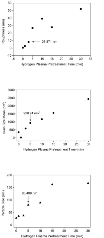
The surface roughness, average grain size and particle size of pretreated Cr films were analyzed by AFM. Fig. 2 shows the surface roughness, average grain size and particle size of Cr films for various periods of treatment with H plasma. Longer pre-treatment resulted in rough-2 er surfaces and larger particles on the Cr film. The surface roughness, average grain size and particle size of a particular Cr film when growing CNTs were 26.871 nm, 928.74 nm2 and 80.409 nm, respectively. These obtained analytic results, which shows the particle size to be the major factor that affects the growth of CNTs. CNTs were experimentally demonstrated to grow by precipitation of carbon from supersaturated transition metal particles and the diameter of CNTs was closely correlated with the size of dispersed metal particles
w8,9x. However, the diffusion model for the growth of
CNTs does not have universal significance and growth conditions can also significantly affect the formation of CNTs w10x.
3.2. Growth of VACNTs
Fig. 3 shows SEM photographs of samples grown on H2 plasma-pretreated Cr film pretreated for various periods. As shown in Fig. 3a, no nanotube was found on the surface of a Cr film pretreated with H plasma2 for 3 min. The VACNTs seem only to have grown on the surface of Cr films pretreated with H2 plasma-pretreated for 5 min or 10 min, as shown in Fig. 3b and c, respectively. These CNTs possess a high-aspect-ratio, implying potential use as field emission devices.
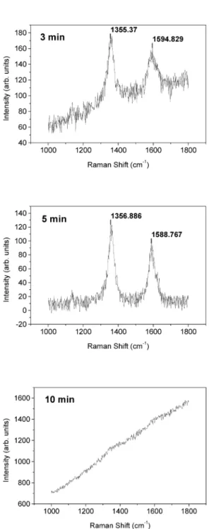
The first-order Raman spectrum of the CNTs includes strong, sharp peaks at 1581 cmy1 (G-line) and 1350
cmy1 (D-line). The peaks suggest that the CNTs are
characteristic of microcrystalline graphite. Fig. 4 dis-plays the Raman spectra of the carbon grown on Cr film with various periods of pre-treatment. As shown in Fig. 4a,b only samples pretreated for 3 and 5 min showed two peaks at approximately 1350 and 1581 cmy1. The relative intensities of the two peaks depend on the type of graphitic material. Normally, the intensity of the 1350 cmy1 peak increases as (i) the amount of disorganized carbon in the samples increases or(ii) the graphite crystal size decreases. However, the SEM pho-tograph in Fig. 3a shows that no CNT grew on the sample with 3 min of H pre-treatment, the peaks seem2 to be associated with amorphous carbon since both resemble those in the Raman spectrum. Furthermore, as shown in Fig. 4c, the Raman spectrum indicates that the sample with 10 min of H pre-treatment did not include2 carbon, which fact is interesting, since this sample looks like carbon tips as shown in Fig. 3c. After further characterized by X-ray diffraction, this sample was verified to be silicon. This maybe due to the surface of
Fig. 1. SEM photographs of bias-enhanced H plasma-pretreated Cr film, obtained for various periods of pre-treatment.2
the silicon wafer appeared after pre-treatment. While in the growth step, lacking for the protection of Cr and the proper catalysts, the silicon sample suffered a more severe anisotropic etching.
The CNTs were analyzed by TEM to confirm that they were truly CNTs, and not carbon fibers. Fig. 5 displays the TEM image of an end section of an
individual CNT. Comparing this image to those present-ed elsewhere, w8x indicates that the tube is a multi-walled CNT. The darkness of the nanotube walls indicates that the nanotube is multi-walled and hollow rather than solid fibers. Fig. 5 also reveals that the CNT has inner diameters of approximately 10 nm and outer diameters of approximately 30 nm. The Cr was also
Fig. 2. Surface roughness, average grain size and particle size of H2
bias-enhanced plasma-pretreated Cr film, obtained for various periods of pre-treatment.
Fig. 3. SEM photographs of samples grown on H plasma-pretreated2
Cr film pretreated for various periods. observed by the EDS attached to the TEM, and is the
darkest and teardrop-shaped part of this image. Acom-parison with the SEM photograph in Fig. 3b suggests that the Cr is on top of the CNT.
In most of the existing models of the chemical vapor deposition, the growth of carbon nanotubes are based on the model, first proposed by Baker et al. w11x: the hydrocarbon molecules decompose at the surface of the
catalyst and the carbon atoms dissolve into the metal, forming a solid solution. When this solution becomes supersaturated, C precipitates at the surface of the particle in its stable form as crystalline graphitic layers. Several reported alignment mechanisms were reviewed to explain the possible mechanism in the deposition process performed here. Bower et al. w12x reported that, the alignment is mainly induced by the electrical self-bias field, imposed on the substrate surface from the plasma environment. However, they used heavier ammo-nia plasma, rather than hydrogen plasma, promoting the establishment of a stronger local field at the surface. They used this fact to explain why others have grown randomly oriented nanotubes in a similar microwave plasma enhanced chemical vapor deposition system
Fig. 4. Raman spectra of samples grown on H plasma-pretreated Cr2
film pretreated for various periods.
Fig. 5. TEM image of the end section of an individual CNT. using hydrogen-based plasma w13,14x. Ahigh
concen-tration of hydrogen plasma and a high negative bias applied to the substrate were found to enable the randomly oriented carbon nanotubes to be easily removed by anisotropic etching. Such a mechanism can remove all carbon nanotubes that are not parallel to the hydrogen plasma attracted to the substrate under a negative d.c. bias w8x. Similarly, Murakami et al. w15x, developed a process that involved depositing and pat-terning a nickel-based metal line on a glass substrate, followed by bias-enhanced microwave plasma chemical
vapor deposition to grow well-aligned carbon nanotubes. During nanotube growth, a negative voltage of y250 V was applied to the substrate. Merkulov et al. w16x reported that the crowing effect could assist the align-ment of CNTs. However, in this study, it could not be decided that the crowing effect or anisotropic etching which was the main mechanism to assist the alignment of CNTs.
3.3. Field emission properties
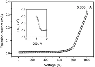
Field emission properties are obtained using a diode structure. An anode, made of indium tin oxide glass, was separated by 500 mm from the tip of a cathode made of CNTs. TheI–V properties were measured using
an electrometer (Keithley 237) and analyzed using the Fowler–Nordheim (F–N) model. Fig. 6 characterizes the VACNTs grown on Cr film pretreated for 5 min. The emission current at an applied voltage of 1000 V was 0.305 mAycm . The macroscopic turn-on field was2 1.7 Vymm. In 1928, Fowler and Nordheim proposed the
model of field emission from a solid w17x. The F–N model states that the relationship between the emitted current in the local electric fieldF and the work function w is Ia(F y2 w) exp(yBw3y2yF), with Bs6.83=10 (V9 eVy3y2 my1x. The local electric field F is not simply Vyd, which is the macroscopic field obtained when a
voltage V is applied between two electrodes separated
by a distance d. Rather, F is, in most cases, larger by
an enhancement factor b, which reflects the ability of the emitter to amplify the field. The factor b is deter-mined mainly by the geometrical shape of the emitter, and the field at the emitter surface is frequently
Fig. 6. Emission current against applied voltage, and F–N plot for CNTs. expressed asFsbEsbVyd, where EsVyd is the
mac-roscopic field. Moreover, literature includes arguments based on values of b that have been determined from the shape of the emitter, and especially from the radius of curvature of the tip, R . The most basic approxima-tip tion is FfVy(kR ), where k is a constant that dependstip on the geometry and is taken to equal 5 for an infinitely long cylindrical emitter w18x. From the aforementioned definition and approximation for F, bsdy(kR ) istip
obtained. Thus,R s30 nm yieldstip b;3000.
4. Conclusions
Using CH4yH source gases, VACNTs were grown2 by microwave plasma chemical vapor deposition on a Cr film, which had been pretreated in bias-enhanced H plasma for 5 min. Following this pre-treatment, the2 Cr film provided the catalysts for growing CNTs. The surface roughness, average grain size and particle size of the pretreated Cr film were 26.871 nm, 928.74 nm2 and 80.409 nm, respectively. The resultant CNTs was vertically aligned; had a notable high-aspect-ratio struc-ture and a diameter of 30 nm. The TEM image indicates that the intrinsic structure is truly that of a CNT and includes teardrop-shaped Cr at the end. The field emis-sion properties of the resultant carbon nanotubes includ-ed an emission current of 0.305 mAat 2 Vymm; and a
turn-on field of 1.7 Vymm.
Acknowledgments
The authors would like to thank the National Science Council of the Republic of China, Taiwan for financially
supporting this work under Contract No. NSC 91-2219-E-009-029.
References
w1x W.A. de Heer, A. Chatelain, D. Ugarte, Science 270 (1995)
1190.
w2x J.M. Bonard, J.P. Salvetat, T. Stockli, L. Forro, Appl. Phys.
Lett. 75(1999) 873.
w3x Z. Yao, C.L. Kane, C. Dekker, Phys. Rev. Lett. 84 (2000)
2941.
w4x E.W. Wong, P.E. Sheehan, C.M. Lieber, Science 277 (1997)
1972.
w5x S. Iijima, Nature 354(1991) 56.
w6x Z.P. Huang, J.W. Xu, Z.F. Ren, J.H. Wang, M.P. Siegal, P.N.
Provencio, Appl. Phys. Lett. 73(1998) 3845.
w7x M. Okai, T. Muneyyochi, T. Yanguchi, S. Sasaki, Appl. Phys.
Lett. 77(2000) 3468.
w8x S.H. Tsai, C.W. Chao, C.L. Lee, H.C. Shih, Appl. Phys. Lett.
74(1999) 3462.
w9x R. Andrew, D. Jacques, A.M. Rao, F. Derbyshire, D. Qian, X.
Fan, E.C. Dickey, J. Chen, Chem. Phys. Lett. 303(1999) 467. w10x Y.Y. Wei, G. Eres, V.I. Merkulov, D.H. Lowndes, Appl. Phys.
Lett. 78(2001) 1394.
w11x R.T.K. Baker, M.A. Barber, P.S. Harris, F.S. Feates, R.J. Waite,
J. Catal. 26(1972) 51.
w12x C. Bower, W. Zhu, S. Jin, O. Zhou, Appl. Phys. Lett. 77 (2000) 830.
w13x L.C. Qin, D. Zhou, A.R. Krauss, D.M. Gruen, Appl. Phys.
Lett. 72(1998) 3437.
w14x O.M. Kuttel, O. Groening, C. Emmenegger, L. Schlapbach,
Appl. Phys. Lett. 73(1998) 2113.
w15x H. Murakami, M. Hirakawa, C. Tanaka, H. Yamakawa, Appl.
Phys. Lett. 76(2000) 1776.
w16x V.I. Merkulov, A.V. Melechko, M.A. Guillorn, D.H. Lowndes,
M.L. Simpson, Appl. Phys. Lett. 79(2001) 2970.
w17x R.H. Fowler, L.W. Nordheim, Proc. R. Soc. London Ser. A
119(1928) 173.
w18x W.P. Dyke, W.W. Dolan, Adv. Electron. Electron. Phys. 8 (1956) 89.