Film structure and ferroelectric properties of vanadium-doped Sr 0.8 Bi 2.3 Ta 2 O 9
thin films
San-Yuan Chen, Bang-Chiang Lan, and Chang-Sheng Taso
Citation: Journal of Applied Physics 91, 10032 (2002); doi: 10.1063/1.1480110
View online: http://dx.doi.org/10.1063/1.1480110
View Table of Contents: http://scitation.aip.org/content/aip/journal/jap/91/12?ver=pdfcov
Published by the AIP Publishing
Articles you may be interested in
Soft chemical deposition of Bi Fe O 3 multiferroic thin films
Appl. Phys. Lett. 90, 052906 (2007); 10.1063/1.2433027
Effect of incorporating nonlanthanoidal indium on the ferroelectric performance of Bi 4 Ti 3 O 12 thin films
Appl. Phys. Lett. 89, 072903 (2006); 10.1063/1.2219138
Retention characteristics in Bi 3.25 La 0.75 Ti 3 O 12 thin films prepared by the polymeric precursor method
Appl. Phys. Lett. 86, 112909 (2005); 10.1063/1.1886893
Ferroelectric properties of 0.87 Na 0.5 Bi 0.5 Ti O 3 – 0.13 Pb Ti O 3 thin film prepared by metalorganic solution deposition
Appl. Phys. Lett. 85, 3190 (2004); 10.1063/1.1802382
Fatigue-free behavior of highly oriented Bi 3.25 La 0.75 Ti 3 O 12 thin films grown on Pt/Ti/SiO 2 /Si (100) by metalorganic solution decomposition
Appl. Phys. Lett. 78, 658 (2001); 10.1063/1.1333686
be attributed to the enhanced densification due to the addition of vanadium. With partial substitution of tantalum by vanadium up to x⫽0.15, a larger remanent polarization (2Pr) of 30.5C/cm2can be obtained for the Sr0.8Bi2.3Ta1.85V0.15O9film at 800 °C that is attributed to the larger grain size and
increased ‘‘rattling space.’’ Furthermore, the vanadium substitution for tantalum ion can effectively reduce the leakage current density as lower as 5⫻10⫺8A/cm2 at an applied electric field of 100 kV/cm because of the reduced mobility of charge carriers. However, the incorporation of vanadium does not cause appreciable negative effect on the fatigue endurance of Sr-deficient Sr0.8Bi2.3Ta2O9
films until more than 20 mol % (x⫽0.2) vanadium was added. © 2002 American Institute of Physics. 关DOI: 10.1063/1.1480110兴
I. INTRODUCTION
SrBi2Ta2O9 共SBT兲 is one of the most promising materi-als for application to nonvolatile random access memories due to its excellent ferroelectric properties, characterized by limited polarization fatigue and low coercive field.1,2 SBT belongs to the family of Aurivillius compounds with a gen-eral formula of (Bi2O2)⫹2(Am⫺1BmO3m⫹1)2⫺, consisting of
m-perovskite units sandwiched between bismuth oxide lay-ers.共Here A and B are the two types of cations that enter the perovskite unit. A is Bi⫹3, Ba⫹2, Sr⫹2, Pb⫹2, or K⫹1; B is Ti4⫹, Ta⫹5, Nb5⫹, Mo6⫹, or W6⫹.兲3,4 The ferroelectric properties, crystal structure and microstructure are remark-ably influenced by the composition fluctuation. Atsuki et al.5 reported that the remanent polarization ( Pr) of SrxBi2zTa2O9
共0.7⭐x⭐1.0, 2.0⭐2z⭐2.6兲 increased with the decrease of the Sr/Ta mole ratio for films annealed at 800 °C. A maxi-mum remanent polarization was also reported for the SBT films with 20 mol % Sr-deficient and 10 mol % Bi-excess composition.6,7 The enhancement in Pr with decreasing Sr content from x⫽1.0– 0.8 was attributed to the increase in grain growth. Watanabe et al. reported that the dependence of Pron Sr content in SrBi2Nb2O9 共SBN兲 films was entirely
due to the sensitivity of grain orientation to Sr content.8The randomly oriented Sr-deficient SBN films have larger rema-nent polarization than c-axis oriented stoichiometric SBN films. However, the high postannealing temperatures and the low remanent polarization of SBT films are two major bar-riers for their application to random access memories.9
Many physical properties of materials may vary signifi-cantly with a subtle change of chemical composition through doping or substituting of desired impurities. The Nb substi-tution for Ta was also used to enhance the ferroelectric
properties.10,11The partial substitution of Sr2⫹ by Ba2⫹ has resulted in the noticeable improvement of the dielectric con-stant and remanent polarization was also observed.12An en-hanced remanent polarization was also observed in the SBT film with the addition of Pb2⫹cation.13
Although the Sr-deficient SBT films have been reported to exhibit more excellent polarization compared to stoichio-metric SBT films; little work has been done to investigate the role of B-site substitution in Sr-deficient SBT system. Sev-eral works demonstrate that the additive usually plays an important role in grain growth and has a remarkable effect on electrical properties of materials especially for electronic ceramics.14 Vanadium oxide 共Tm⫽⬃690 °C兲 or vanadium-based multiple oxide system are reported to have lower melt-ing point and used as one effective sintermelt-ing aid for low-firing ceramics.15,16 Therefore, vanadium-doped SBT films were chosen to investigate the effect of vanadium incorpora-tion on the structure, surface morphology, and electrical properties of Sr-deficient Sr0.8Bi2.3Ta2O9 thin films.
II. EXPERIMENT
The starting materials for the metalorganic decomposi-tion process were bismuth 2-ethylhexanoate
兵Bi关CH3(CH2)3CH共C2H5)COO]3其, strontium 2-ethylhexanoate 兵Sr关CH3(CH2)3CH共C2H5)COO]2其, vana-dium isopropoxide V共OC3H7)5 and tantalum ethoxide 关Ta共OC2H5)5] with 2-ethylhexanoic acid as the solvent. The
metalorganic precursors were mixed to form solutions with compositions of Sr0.8Bi2.3(Ta2⫺xVx)O9. 共SBTV兲. Prior to
film deposition, the substrate (Pt/Ti/SiO2/Si) was cleaned in
acetone and alcohol ultrasonic baths, then blown dry with N2
gas. The solutions were spin coated onto the substrate at a speed of 3000 rpm. After each coating, the as-deposited film was dried on a hot plate at a temperature about 350 °C to
a兲Electronic mail: [email protected]
10032
0021-8979/2002/91(12)/10032/6/$19.00 © 2002 American Institute of Physics
remove the solvent before application of the next coating. After the process was repeated four times, the as-deposited films were sintered at 500– 850 °C in air for 30 min by di-rectly placing the coated substrate into a preheated tube fur-nace. Most of the data reported here were obtained for films with four layers (t⫽0.37– 0.4m).
The crystal structures of the films were analyzed by us-ing Siemens D5000 x-ray diffraction共XRD兲 with Cu K␣ ra-diation and a Ni filter. The chemical composition of the films was determined using inductively coupled plasma mass spec-troscopy 共Perkin Elmer, SCIEX ELAN 5000兲. The film thickness was measured by Dektak surface profilometer. Field-emission scanning electron microscopy共FESEM兲 共Hi-tachi S4000兲 was performed to investigate the surface mor-phology of the films. Patterned top Au electrodes were sput-ter deposited onto the SBT layers through a shadow mask on an area of 8.0⫻10⫺4cm2 area to define capacitors. A ferro-electric testing system 共RT-66A, Radiant Technologies Inc.兲 operating in the virtual-ground mode was used to obtain the remanent polarization ( Pr)-coercive field (Ec) hysteresis characteristics. Fatigue tests of the films were conducted us-ing a bipolar square wave of 5 V at 1 MHz.
III. RESULTS AND DISCUSSION A. Microstructure and phase evolution
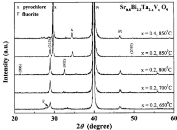
XRD analysis was used to investigate the effect of vana-dium content on the structural development of Sr0.8Bi2.3(Ta2⫺xVx)O9 films (0⭐x⭐0.8) annealed at 800 °C
for 0.5 h. As shown in Fig. 1, both intensity and sharpness of the共115兲 oriented peak were enhanced with increasing vana-dium content in the range of x⫽0 – 0.2 content, suggesting an increase in grain size compared to Sr0.8Bi2.3Ta2O9without vanadium. The共115兲 reflection is slightly shifted to the lower diffraction angle, indicating that the V ions could be dis-solved into TaO6 octahedral structure to substitute for Ta
ions. Nevertheless, with the addition of vanadium content above 0.2, the共115兲-oriented peak intensity was rapidly de-creased along with the accelerating formation of the pyro-chlore phase 共labeled as x phase in Fig. 1兲, indicating the layered perovskite structure became unstable. The
pyro-chlore phase was similar to Bi-deficient pyropyro-chlore as re-ported by Rodriguez et al.17 XRD studies of Sr0.8Bi2.3(Ta1.8V0.2)O9 films also indicate that the films an-nealed at 500 °C are amorphous. From 600 °C, a broad dif-fraction peak appears at around 2⫽28.5, which indicates that a mixture phases of fluorite and perovskite are evolved from the amorphous SBTV films. At 650 °C, as shown in Fig. 2, a strong 共115兲 diffraction peak along with a small broad matrix are formed, which indicates that the films are not fully crystallized. However, at 700 °C, well-crystallized perovskite phase has been completely developed in the Sr0.8Bi2.3(Ta1.8V0.2)O9 thin films, which is much lower than
that of Sr0.8Bi2.3Ta2O9 films without doping vanadium. In
other words, the addition of vanadium lowers the annealing temperature and promotes the crystallization of layered-structure ferroelectric SBTV films. At 850 °C, the diffraction peak around 29.5° labeled with x phase in Fig. 2 becomes stronger and the共115兲 peak of perovskite phase almost dis-appears. Even at 800 °C, as the vanadium content 共x兲 was added more than 0.4 in the SBTV film, complete pyrochlore phase with no trace of perovskite has been developed. On the contrary, at 850 °C, although the pyrochlore phase can be detected for the undoped SBT films (x⫽0), the film is pri-marily composed of perovskite phase. The findings imply that the addition of vanadium causes perovskite-SBTV more unstable.
Figure 3 illustrates typical共FESEM兲 surface images ob-tained from SBTV films having various vanadium contents and heated at 800 °C. The microstructure of SBT (x⫽0) film presents a rod-like grain matrix. With the addition of vana-dium, a dense microstructure consisting of larger and sheet grains was observed for the SBTV films with x⬍0.4. How-ever, an increase of vanadium content 共i.e., x⫽0.4兲 leads to the reduction of grain size and the formation of pyrochlore phase. Typical SEM microstructure of SBTV (x⫽0.2) films annealed at 650– 850 °C was shown in the Fig. 4. The film at 600 °C presents featureless microstructure. At 650 °C, a mi-crostructure consisting of rod-like grain matrix with some bright micrograins intervened in between grain boundaries was observed, indicating SBTV perovskite phase has been FIG. 1. XRD patterns of SBTV films annealed at 800 °C for 0.5 h. FIG. 2. XRD patterns of Sr
0.8Bi2.3(Ta1.85V0.15)O9films annealed at different
temperature for 0.5 h.
10033
J. Appl. Phys., Vol. 91, No. 12, 15 June 2002 Chen, Lan, and Taso
crystallized from the matrix. The micrograins are probable flourite phase as corresponding to the XRD pattern marked with arrow in Fig. 2. At 750 °C, the cluster grains are merged together to form larger sheet grains, which is probably re-lated to the lower melting point of vanadium-based oxide. The average grain size were measured to be about 300– 400 nm. At 850 °C, the microstructure exhibits different bright polygonal grains mixed with dark lump area that should be pyrochlore phase or other secondary phases in accordance to the XRD patterns of Fig. 2.
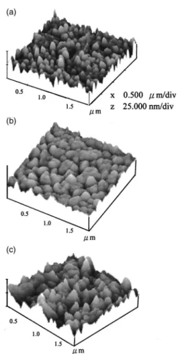
The atomic force microscopy 共AFM兲 images in Fig. 5 indicate that the surface morphology of the 800 °C-annealed SBTV with x⫽0.2 film exhibits smooth. It could be eluci-dated with the fact that the addition of low melting-point vanadium-based content makes SBTV film relatively easy to merge small grains into large and flat grains during high-temperature annealing. However, excess vanadium 共at x ⭓0.4兲 may induce the Ti outdiffused from the substrate to react with SBTV film to form pyrochlore phase and thus the film morphology becomes rather rough.
B. Ferroelectric properties
Ferroelectric hysteresis measurements were conducted on Sr0.8Bi2.3(Ta2⫺xVx)O9 thin films in metal/ferroelectric/
metal configuration at an applied voltage of 6 V using stan-dardized RT 66A ferroelectric test system. The typical
hys-FIG. 3. SEM surface micrographs of SBTV with共a兲 x⫽0, 共b兲 x⫽0.2, 共c兲
x⫽0.4, and 共d兲 x⫽0.8 films annealed at 800 °C for 0.5 h.
FIG. 4. Phase evolution of Sr0.8Bi2.3(Ta1.85V0.15)O9films annealed at 850 °C for共a兲 5, 共b兲 10, 共c兲 30, and 共d兲 60 min.
FIG. 5. Atomic force micrographs of SBTV with共a兲 x⫽0, 共b兲 x⫽0.2, 共c兲
x⫽0.4 films annealed at 800 °C for 0.5 h.
teresis loops of Sr0.8Bi2.3(Ta1.85V0.15)O9 films annealed at
700– 800 °C are shown in Fig. 6. It was observed that the saturated hysteresis loops have been developed from the films annealed at 700– 800 °C that can be attributed to the enhanced densification due to the addition of vanadium. As illustrated from the SEM images in Fig. 3 for 700– and 800 °C-annealed SBTV films, it can be observed that the grain size of the film at 800 °C is larger but the density shows little difference compared to 700 °C-annealed film. However, the remanent polarization (2 Pr⫽21.9C/cm2) of the Sr0.8Bi2.3(Ta1.85V0.15)O9 films annealed at 700 °C is
lower than that (2 Pr⫽30.5C/cm2) at 800 °C. The larger grain size is the cause of the larger Pr value for the SBTV films annealed at 800 °C.
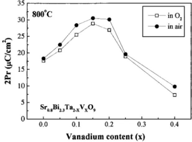
Figure 7 illustrates that the 800 °C-annealed SBTV films prepared from precursor solution with an addition of vana-dium less than 0.3 exhibit better ferroelectric properties com-pared to Sr0.8Bi2.3Ta2O9 thin films. The maximum 2 Prvalue occurs at the SBTV films with x⫽0.15. Above that (x ⫽0.15), the remanent polarization was found to decrease with increasing vanadium content. The measured remanent polarization (2 Pr) values are 30.5C/cm2and 18.1C/cm2, respectively, for Sr0.8Bi2.3(Ta1.85V0.15)O9and Sr0.8Bi2.3Ta2O9
thin films. The improved polarization may be partially attrib-uted to the enhanced grain growth as observed in the SEM micrographs 共Fig. 3兲. Besides the effect of grain size, other
effects to account for variation in remanent polarization have to be considered. According to the report of Subbarao for the layered perovskite structure,18 the enhanced ferroelectric properties in the SBTV films could be well explained by increasing ‘‘rattling space’’ due to the substitution of vana-dium for tantalum because pentavalence vanavana-dium ions (V5⫹, 0.58 Å兲 have a much smaller size compared with nio-bium ions共Ta5⫹, 0.64 Å兲.19However, because V5⫹can have
six coordination of oxygen, it is too small to form a stable layered perovskite structure. As revealed by Wu and Cao, with niobium共Nb5⫹, 0.69 Å兲 substituted by vanadium up to 10 mol % (y⫽0.1) in the strontium bismuth vanadium nio-bate关SrBi2(Nb1⫺yVy)2O9兴 ceramics, the layered perovskite
structure can be preserved.16 Therefore, in the present work, the peroskite structure is still retained for Sr0.8Bi2.3(Ta2⫺xVx)O9 of x⫽0.2 films but for the SBTV
films with the addition of vanadium more than 0.2, i.e., x ⫽0.4, the structure becomes so unstable and the pyrochlore phase is induced. Therefore, the remanent polarization in-creases significantly from 2 Pr⫽18.1C/cm2 for SBT films without vanadium doping to 2 Pr⫽30.5C/cm2 for SBTV films of x⫽0.15 and then rapidly drops to 2Pr ⫽9.8C/cm2 for SBTV films of x⫽0.4.
C. Leakage current
In general, the occupation of Bi on Sr site often occurs in the Sr-deficient SBT compositions since both radii of Sr2⫹
and Bi3⫹are very close, where some fraction of the positive
charged BiSr䊉 ions might be compensated by electrons.20,21 Therefore, by considering only the most probable defects, Sr-deficient SBT films are characteristic of n type. In our work, a reduced leakage current shown in Fig. 8 was ob-served for the Sr-deficient SBT films with increasing vana-dium up to x⫽0.15. The phenomenon reveals that the con-centration and mobility of intrinsic charge carrier in the Sr-deficient SBT films may decrease due to the incorporation of vanadium cation because a decreased leakage current sug-gests a reduced concentration of charge carriers. However, if it was assumed that only pentavalent vanadium cation exist in the SBTV films after air annealing, no appreciable oxygen vacancies are created for the samples with vanadium doping. Therefore, the decreased leakage current could be explained by two possible mechanisms. One is that the reduced mobil-FIG. 6. Hysteresis loops of Sr0.8Bi2.3(Ta1.85V0.15)O9 films annealed at 700
and 800 °C for 0.5 h at an applied voltage of 6 V.
FIG. 7. Remanent polarization (2 Pr) of vanadium-doped SBTV films
an-nealed at 800 °C for 0.5 h at an applied voltage of 6 V.
FIG. 8. Current density of vanadium-doped SBTV films at 100 kV/cm elec-tric field.
10035
J. Appl. Phys., Vol. 91, No. 12, 15 June 2002 Chen, Lan, and Taso
ity of charge carriers may result from the distortion and com-plexity in the crystal structure due to the substitution of tan-talum by smaller vanadium ion. As the vanadium doping concentration exceeds a critical point, the perovskite struc-ture becomes unstable and even destructive, resulting in py-rochlore phase formation as evidenced in Fig. 1. Conse-quently, an increased leakage current was observed in the SBTV films added with vanadium 共x兲 exceeding 0.3.
Another possibility is that the vanadium doping does not only enhance densification but also make film surface smooth. As shown in Fig. 5, the AFM analysis of the SBTV films shows that the SBTV films of x⬍0.3 exhibit flat and dense microstructure. Above that concentration (x⫽0.3), the film surface becomes rather rough, implying that the films have higher leakage current. Therefore, the lowest leakage current occurs at the SBTV film with x⫽0.15 composition. The leakage current of Sr0.8Bi2.3(Ta1.85V0.15)O9 films was
measured around 5⫻10⫺8A/cm2 at an electric field of 100 kV/cm, much lower than that (1.5⫻10⫺6A/cm2) of undoped SBT film by proximately one and half orders of magnitude.
D. Fatigue behavior
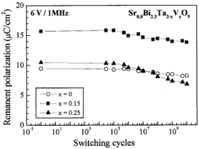
Ferroelectric thin films of bismuth-containing layered perovskite such as SrBi2Ta2O9 and SrBi2Nb2O9 have been
reported to have excellent good fatigue resistance. Fatigue endurance was tested with 1 MHz bipolar pulses at 6 V. Figure 9 shows the fatigue behavior of SBTV 共x⫽0, 0.15, and 0.25兲 films prepared at 800 °C for 0.5 h. Although Sr-deficient Sr0.8Bi2.3Ta2O9film shows an optimal remanent
po-larization of Pr⫽9.7C/cm2, a loss of P
r of 12% was mea-sured after 1010cycles. On the other hand, for the SBT films
with vanadium added (x⫽0.15), no rapid fall off in the Pr value was observed up to about 108 cycles, but the decay in Pr was about 10% of the initial value after 1010cycles. This indicates that the incorporation of limited vanadium into the layered perovskite structure does not cause appreciable fa-tigue. However, the decay in remanent polarization becomes apparent with increasing vanadium content above 20 mol % (x⫽0.2) such as Sr0.8Bi2.3(Ta1.75V0.25)O9 film, indicating
that the addition of vanadium seems detrimental to fatigue resistance of SBT films. There are several proposals that
at-switching because of the structural complex. Further work is underway to understand the effect of vanadium doping on the fatigue properties of the SBT-based layered perovskite structures.
IV. CONCLUSIONS
共1兲 Enhanced ferroelectric properties and lower process-ing temperature of Sr0.8Bi2.3Ta2O9 films deposited on
Pt/Ti/SiO2/Si substrates can be obtained by doping
vana-dium.
共2兲 The measured remanent polarization (2Pr) values increases from 18.1C/cm2for Sr0.8Bi2.3Ta2O9 film to 30.5
C/cm2for Sr0.8Bi2.3Ta1.85V0.15O9 film at an applied voltage of 6 V, respectively.
共3兲 The incorporation of vanadium doping can lead to an increase in leakage resistance of Sr0.8Bi2.3Ta2O9 film. The
leakage current as lower as 5⫻10⫺8A/cm2 can be obtained at an applied electric field of 100 kV/cm.
共4兲 The substitution of limited vanadium for tantalum does not cause appreciable fatigue. However, the addition of more than 20 mol % vanadium seems to adversely affect the fatigue resistance of Sr0.8Bi2.3Ta2O9films due to large lattice
distortion.
ACKNOWLEDGMENT
The authors gratefully acknowledge the National Sci-ence Council of the Republic of China for its financial sup-port through Contract No. NSC90-2215-E-009-061.
1C. A. Paz de Araujo, J. D. Cuchiaro, M. C. Scott, L. D. McMillan, and J. F. Scott, Nature共London兲 374, 627 共1995兲.
2
O. Auciello, J. F. Scott, and R. Ramesh, Phys. Today 51, 22共1998兲. 3G. A. Smolenskii, V. A. Isupov, and A. I. Agranovskaya, Sov. Phys. Solid
State 1, 149共1959兲.
4G. A. Smolenskii, V. A. Isupov, and A. I. Agranovskaya, Sov. Phys. Solid State 3, 651共1961兲.
5T. Atsuki, N. Soyama, T. Yonezawa, and K. Ogi, Jpn. J. Appl. Phys., Part 1 34, 5096共1995兲.
6T. Noguchi, T. Hase, and Y. Miyasaka, Jpn. J. Appl. Phys., Part 1 35, 4900 共1996兲.
7
T. Hase, T. Noguchi, K. Amanuma, and Y. Miyasaka, Integr. Ferroelectr.
15, 127共1997兲.
8K. Watanabe, M. Tanaka, E. Sumitomo, K. Katori, H. Yagi, and J. F. Scott, Appl. Phys. Lett. 73, 126共1998兲.
9
J. F. Scott, in Thin Film Ferroelectric Materials and Devices, edited by R. Ramesh共Kluwer, Norwell, MA, 1997兲, p. 115.
10H. Watanabe, T. Mihara, H. Yoshmori, and Carlos A. Paz de Araujo, Jpn. J. Appl. Phys., Part 1 34, 5240共1995兲.
11A. Furuya and J. D. Cuchiaro, J. Appl. Phys. 84, 6788共1998兲. 12
C. H. Lu and C. Y. Wen, J. Eur. Ceram. Soc. 20, 739共2000兲. 13S. Y. Chen and V. C. Lee, J. Appl. Phys. 87, 8024共2000兲. 14D. M. Smyth, Prog. Solid State Chem. 15, 145共1984兲.
FIG. 9. Fatigue behavior of Sr0.8Bi2.3(Ta2⫺xVx)O9 films with an applied
voltage of 6 V at 1 MHz.
15S. Cho, H. Yoon, D. Kim, T. Kim, and K. Hong, J. Am. Ceram. Soc. 81, 3038共1998兲.
16Y. Wu and G. Cao, Appl. Phys. Lett. 75, 2650共1999兲.
17M. A. Rodriguez, T. J. Boyle, B. A. Hernandez, C. D. Buchheit, and M. O. Eatough, J. Mater. Res. 11, 2282共1996兲.
18E. C. Subbarao, Integr. Ferroelectr. 12, 33共1996兲.
19R. D. Shannon and C. T. Prewitt, Acta Crystallogr., Sect. B: Struct. Crys-tallogr. Cryst. Chem. B25, 925共1969兲.
20C. Voisard, D. Damjanovic, and N. Setter, J. Eur. Ceram. Soc. 19, 1251 共1999兲.
21A. D. Rae, J. G. Thompson, and R. L. Withers, Acta Crystallogr., Sect. B: Struct. Sci. B48, 418共1992兲.
22K. Tominaga, A. Shirayanagi, T. Takagi, and M. Okada, Jpn. J. Appl. Phys., Part 1 32, 4082共1993兲.
23
I. K. Yoo and S. B. Desu, Integr. Ferroelectr. 3, 365共1993兲.
24W. L. Warren, D. Dimos, B. A. Tuttle, R. D. Nasby, and G. E. Pike, Appl. Phys. Lett. 65, 1018共1994兲.
10037
J. Appl. Phys., Vol. 91, No. 12, 15 June 2002 Chen, Lan, and Taso