E L S E V I E R Materials Chemistry and Physics 45 (1996) 284-287
MATERIALS
CHEMISTRYAND
PHYSICS
Materials Science Communication
Deposition properties of selective tungsten chemical vapor deposition
Wen-Kuan Yeh a, Mao-Chieh Chen a, Pei-Jan Wang b, Lu-Min Liu b, Mou-Shiung Lin b
Department oj" Electronics Engineeriizg, Nati(ma! Chiao Tung University, and National Nam~ Device Laboratory, 1001 University Rd., Hsinchu, Taiwan,ROC
b Taiwal~ Semiconductor Mamtj~cturing Company, Hsilwhu, Taiwan, ROC
Received 19 December 1994; accepted 17 November 1995
Abstract
This work investigates the basic deposition properties of selective tungsten chemical vapor deposition (W-CVD) using the process of silane reduction of WF6 with the SiH4/WF 6 flow rate ratio less than 0.6 over the temperature range 280-350 °C. Selective W-CVD was performed on a contact hole patterned silicon substrate with in situ NF 3 plasma etching of the silicon substrate prior to the selective tungsten deposition. The W deposition rate, deposition selectivity and W film resistivity were investigated with respect to the Sill4 partial pressure, WF6 partial pressure, total (Sill4 + WF~) deposition pressure, as well as the flow rate of the hydrogen carrier gas. It was found that the deposition rate is proportional to the Sill4 partial pressure. With a constant SiH4/WF~ flow rate ratio, the deposition rate increases with total pressure. At given flow rates of Sill4 and WF6, the deposition rate and film resistivity are dependent on the flow rate of the carrier gas. The experimental results show that the reverse bias junction leakage for the wet etching pretreated W/p ÷-n junction diode is smaller than that of the plasma pretreated diode. On the other hand, the contact resistance of the AI/W/n + p diode is smaller than that of the A1/W/p+n diode.
Keywords: Deposition; Tungsten chemical vapor deposition; Silane reduction; Resistivity
1. I n t r o d u c t i o n
Selective tungsten chemical vapor deposition (W-CVD) is one of the most attractive techniques for filling deep sub- micron contact holes for ULSI applications. Selective W- CVD can be performed using hydrogen (H2) reduction [ 1 ] or silane (SiH.~) reduction [2,3] of tungsten hexafluoride ( W F 6 ) .
Selective W-CVD using the Ha-reduction process suffers from the high reactivity of WF6 toward the silicon substrate. This causes excessive Si consumption, encroachment at the Si/SiO: interface, and wormhole formation in the contact regions [4,5]. These disadvantages do not occur in the silane reduction process [6]. Nonetheless, in both processes, the first reaction that occurs between Si and WF6 is the so-called Si displacement reaction [7]. During the Si displacement reaction, WF6 first dissociates on the Si surface, forming WFx (x < 6) adsorbed on the surface, and then further reduces to W. At the same time, Si is converted into SiFx ( x > 1) and further changes to SiF 4. The reaction products (e.g., WF~ and SiF4) that can induce selectivity loss must be removed [8]. Thus Si reduces the WF¢ molecules, leading to the deposition of a W film. As the tungsten surface adsorbs more WF~ species, this highly fluorinated surface would react with Sill4 0254-0584/96/$15.00 © 1996 Elsevier Science S.A. All fights reserved SSDI 0254-0584( 95)01736-4
to form further W film, leaving SiF4 and Ha on the surface [9].
In the Sill4 reduction process, the chemical reaction of the SiH4/WFr, system is rather complicated. For selective W- CVD, the major problem is the lack of understanding and control of the selectivity loss. The most important parameters for the deposition selectivity of the SiH4/WF6 chemistry are the deposition temperature and the reactant flow rate. This work investigates the basic deposition properties of selective W-CVD using the Sill4 reduction process. The deposition conditions of tungsten for submicron contact hole filling were investigated. The electrical characteristics of the W contacted shallow junction were also studied.
2. Experimental
The starting material was p-type (100) oriented Si wafers with 8-12 ~ cm nominal resistivity and n-type (100) ori- ented Si wafers with 10-20 ~ cm nominal resistivity. After RCA standard cleaning, the wafers were thermally oxidized to grow an oxide layer with a thickness of 1500 X, followed by deposition of 4500-,~-thick BPSG. Diffusion areas with sizes ranging from 2 0 0 × 2 0 0 to 1200X 1200 ~m were
W.-K. Yeh et al. /Materials Chemistpy and Physics 45 (1996) 284-287 285
defined on the oxide covered wafers using the conventional photolithographic technique.
For the p +n junction, the junction implant was carried out by BF2 + implantation on the n-type substrate at 30 keV to a dose of 3 × 10 ~5 cm -2 followed by furnace annealing at 900 °C for 30 rain in N2 ambient. For the n +p junction, the junc- tion implant was carried out by As + implantation at 50 keV to a dose of 5 × 10 ~5 cm -2 followed by furnace annealing at 950 °C for 30 min in N2 ambient. A 6000-A.-thick TEOS layer was then deposited on all the wafers, and contact holes with sizes ranging from 0.6 to 5 b~m were defined on the wafers using the conventional photolithographic technique. Prior to conducting the selective W-CVD, the wafers were dipped in dilute HF (2%) solution for 30 s, followed by a rinse in deionized water for 2 min. The wafers were then loaded into the load-locked cold wail W-CVD system within 5 rain to avoid the formation of native oxide on the Si surface.
An in situ predeposition plasma etching was conducted using the following conditions: r.f. power 30 W, total gas pressure 100 mtorr, NF3 flow rate 12 sccm, and N2 flow rate 72 sccm. After the plasma etching, the wafers were trans- ferred from the plasma etching chamber to the tungsten dep- osition chamber without being exposed to the atmosphere. In addition, a number of substrate wafers prepared for investi- gation of the diodes' current-voltage characteristics with respect to the tungsten predeposition treatment of the Si sub- strate were not subjected to the plasma etching procedure. The base pressure of the CVD chamber was 10 .6 tort.
In this work, the W-CVD was conducted using the follow- ing conditions: substrate temperature 280-400 °C, total gas pressure 100 mtorr, WF6 flow rate 20-30 sccm, Sill4 flow rate 10-20 sccm, and H2 carrier gas flow rate 0-1400 sccm. After the selective W-CVD, A1 metallization was applied, followed by 30 min sintering at 400 °C. The thickness of tungsten-filling in the contact hole was determined from the cross-sectional scanning electron microscopy (SEM) micro- graph. The W-CVD selectivity was examined using an optical microscope in the dark field mode. The contact resistance was measured using the four-terminal Kelvin structure as well as the contact chain structure.
tion of Si and more severe encroachment at the S i / S i Q interface. Within the selective process window of 280-350 °C, excellent selectivity, with a selectivity loss of less than 1 cm -a, can be obtained using a SiH4/WF 6 flow rate ratio smaller than 0.6.
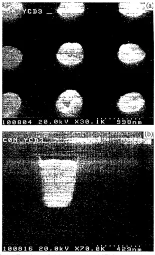
Tungsten can be selectively deposited for submicron con- tact hole filling at a deposition rate as high as 2300 A rain- ~, as shown in Fig. 2. The roughness of the W/Si interface can be quite different for different predeposition substrate surface treatments. For the Sill 4 reduction process, the flow rates of WF6, Sill4 and the carrier gas (H2) were found to greatly
°S
@ 1 0 0 0 0 Deposition Temperature (°C) 400 350 3 2 0 280 i000 O-'O.--.Q, m , m WF6= 20 seem SiII4= 10 sccm H z = I000 sccm Pt,t~l= i00 retort I , 1 l o 0 i i i t 1,4 . 1,5 1,6 1 , 7 . 1.8 1.9 1000/T (K 1)Fig. 1. Dependence of CVD tungsten deposition rate on the deposition temperature.
3. Results and discussion
The Arrhenius plot for selective W-CVD on the submicron contact hole substrate is shown in Fig. 1. The process window for the selective deposition ranged from 280 to 350 °C, with an activation energy of 0.84 eV. In this temperature range, the surface reaction was the dominant process of W-CVD. Higher deposition temperature ( > 350 °C) facilitated the deposition of W atoms on S i Q , because the reaction byprod- uct SiF2 reacts with WF¢ species, leading to the loss of selec- tivity. The morphology of the W film deposited at high temperature has a columnar structure and possesses a higher resistivity. In addition, the high deposition temperature enhanced the Si reduction process, causing higher consump-
Fig. 2. (a) Top-view and (b) cross-sectional SEM micrographs showing selective W deposition for submicron contact hole filling.
286 W.-K. Yeh et al. / Materials Chemistry and Physics 45 (1996) 284-287
influence the tungsten deposition rate and deposition selectivity.
The dependence of the tungsten deposition rate on the Sill 4 flow rate for various fixed WF6 flow rates is shown in Fig. 3. At constant total pressure, the deposition rate is proportional to the Sill.; partial pressure. At a constant SiH4/WF~ flow rate ratio, the deposition rate increases slightly with the total pressure of WF~ and Sill4, as shown in Fig. 4. In addition, the S i H J W F 6 flow rate ratio was found to have a profound effect on the resistivity of the deposited W film. The W film can be categorized as low-resistivity a-type (p < 100 ~.~ cm) or high-resistivity [3-type ( p > 300 >O, cm), depending on the deposition conditions.
Fig. 5 shows the dependence of the tungsten film resistivity on the Sill4 flow rate for various fixed flow rates of WF~. At a deposition temperature of 300 °C, low-resistivity W films with a granular structure (a-type) can be selectively and con formally deposited on submicron contact holes with a low ( < 0 . 6 ) SiH4/WF~ flow rate ratio. On the other hand, at a high SiHa/WF~ flow rate ratio ( > 2), high-resistivity W films with a columnar structure (13-type) were deposited not only on the Si substrate at the bottom of the contact hole but also along the sidewall of the contact hole, leading to W selectivity loss. For a SiH4/WF6 ratio of less than 1, pure W of bulk density and resistivity can be deposited.
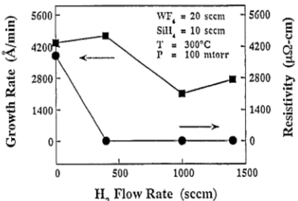
The deposition rate and the film resistivity were also found to be dependent on the carrier gas flow rate of hydrogen, as shown in Fig. 6. At a constant total pressure and fixed flow rates o f W F 6 and Sill4, the partial pressures o f W F 6 and Sill4 will increase as the carrier gas flow rate is lowered. Thus, at a very low flow rate of carrier gas or no carrier gas at all, the increased partial pressures of WF6 and Sill4 would result in the deposition of W particles on the chamber wall of the W- CVD system and also lead to deposition selectivity loss and high-resistivity [3-type film deposition.
The current-voltage characteristics were investigated for the tungsten contacted W / p + n junction diodes, which were fabricated by selective W-CVD on two differently pretreated Si substrates with a defined diode area of 1000× 1000 b~m. At least 40 randomly chosen diodes were measured in each case. Fig. 7 illustrates histograms showing the distribution of the reverse leakage current density measured at - 5 V for the W / p + n junction diodes with two different predeposition sub- strate treatments. For the diodes with a predeposition sub- strate treatment of dilute HF wet etch, the average reverse leakage current density is about 2 nA cm-2. With an addi- tional plasma treatment following the HF wet etch, the diodes' leakage current density was found to be about three times larger than that of the diodes that did not receive the predeposition plasma etching. The plasma etching tended to result in more Si consumption and a rough W/Si interface by the selective W-CVD. This is presumably the main reason for the increased reverse leakage for the shallow junction diodes.
The contact resistance was measured for the A 1 / W / n + p and A l / W / p + n diodes. For the A 1 / W / n + p diode with a
20000
~ " & ,WF6=IO seem - - O - - WE,=20 . . . . / • ,'WF~=24 seem / o 15000 + WF~=30 sccm /
/
~C~ i0000 T = 300'C / P = 100 mtorr / 5000 0 t i i 12 16 20 24Silt 4 Flow Rate (scem)
Fig. 3. Dependence of tungsten deposition rate on the Sill4 flow rate, for various fixed WF,~ flow rates.
7000 $ 6000 °~,~, 5000 2 4000 3000 "~ 2000 i000 0 25 A :SitljWF l ,, 0,4 + S I t I J ' , V F ~ . 0,5 + S l l I , i / W F ~ # 0,6 T ~ T t I 30 35 40 45 50 55 Sill 4 + WF~ Flow R a t e (seem)
Fig. 4. Dependence of tungsten deposition rate on the total flow rate of SiHa and WF6, for various fixed SiH.;/WF~, flow rate ratios.
? 700 ,
' S
+ W F , = 10 seem 600 ....--~- WF~= 20 seem A .WF= 24 sccm 500 .~ : w r y . 30 s e e m 40O 30O 2OO i00 0 l i i o 0.4 0,8 1,2 1,(; S i H 4 / W F ~ F l o w R a t i oFig. 5. Dependence of tungsten film resistivity on the SiH.JWFe flow rate ratio, for various fixed flow rates of WFe,.
2 c~ 5600 t WF= = 20 seem J. ~ SitI~ = 10 sccm 4200~'--- ~ T = 300°C ( .<___ ~ P I00 retort 14000 ~ ~. >" l 500 1000 1500
tI 2 Flow Rate (seem)
5600 4200
2800
1400
0
Fig. 6. Dependence of tungsten deposition rate and tungsten film resistivity on the carrier gas (H2) flow rate.
W.-K. Yeh et al./Materials Chemistry and Physics 45 (1996) 284-287 287 ~. 30~ ~ N 0 . o f D i o d e = 4 0 lO 0 r i r , i i p 50 4o ~. zo I 2 3 5 6 7 10 20
Leakage Current Density (nA/cm z)
Fig. 7. Histograms showing the distribution of reverse leakage current den- sity measured at - 5 V for the W/p + n junction diodes with the Si substrates pretreated with (a) dilute HF wet etching, and (b) dilute HF wet etching followed by plasma etching.
4. C o n c l u s i o n s
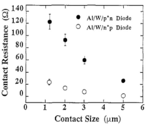
Control of deposition selectivity is a problem of vital importance in the development of selective W-CVD. The experimental results in this work have revealed the selective process window for the Sill 4 reduction process to be as fol- lows: substrate temperature 280-350 °C, total gas pressure 100 mtorr, SiH4/WF 6 flow rate ratio less than 0.6, and H2 carrier gas flow rate 1000 sccm. At a constant total pressure, the W deposition rate, selectivity loss and W film resistivity are all proportional to the deposition temperature, flow rate of Sill4, and total pressure of Sill 4 and WE6. Both the selec- tivity loss and W film resistivity increase with decreasing flow rate of the hydrogen carrier gas. Prior to the W-CVD, a proper substrate surface treatment must be performed. Better I-Vcharacteristics were found for the W / p + nj unction diodes with the Si substrates wet etched in dilute HF rather than etched in NF 3 plasma prior to the selective W-CVD. The contact resistance of the A1/W/n +p diode is about five times Iower than that of the A1/W/p+n diode, which implies a large segregation of arsenic atoms at the W/Si interface.
,-, 140 I "-" 120i 100
,~
80 60 -~ 40 20 0 i i l ~ i i~ • AI/W/p*n D i o d e © AI/W/n"p D i o d e 0 • O O © Contact Size (~tm)Fig. 8. Contact resistance as a function of contact size for (O) AI/W/p+n and (O) A l / W / n + p diode structures.
contact area of 2 X 2 ~m, the measured contact resistances are about 20 and 120 f~, using the four-terminal Kelvin struc- ture and the contact chain structure, respectively. The larger contact resistance measured by the contact chain structure is due to the contribution from the n + diffusion layer. Fig. 8 shows the measured contact resistance versus contact size using the Kelvin structure. The contact resistance of the A1/ W / p + n diode is about five times higher than that of the AI/ W / n + p diode; this is presumably due to the fact that the As atoms are largely segregated at the W/Si interface.
A c k n o w l e d g e m e n t s
This work was supported by the National Science Council (ROC) under Contract No. NSC83-0425-E009-001-1.
R e f e r e n c e s
[ 1] C.M. Mclonica and K. Krishnamani, J. Electrochem. Soc., 133 (i986) 2542.
[2] R.F. Foster, S. Tseng, L. Lane and K.Y. Ahn, in Tungsten Workshop III, Materials Research Society, New York, 1988, p. 69.
[3] Y. Kusumoto, K. Takakuwa, H. Hashinokuchi, T. Ikuta and I. Nakayama, in Tungsten Workshop III, Materials Research Society, New York, 1988, p. 103.
[4] W.T. Stacy, E.K. Broadbent and M.H. Norcott, J. Electrochem. Soc., 132 (1985) 444,
[5] R.A. Levy, M.L. Green, P.K. Gallagher and Y.S. AIi, J. EIectrochem. Soc, 133 (i986) i905.
[6] R.S. Rosler, J. Mendonca and M.J. Rice Jr., J. Vac. Sci. Technoi. B6 (1988) 1721.
[7] E.K. Broadbent and C.L. Ramiller, J. Electrochem. Soc., 131 (1984) 1427.
[8] P. Lami and Y. Pauleau, J. Electrochem. Soc., 135 (1988) 980. [9] M.L. Yu and B.N. Eldridge, J. Vac. Sci. Technol. A7 (1989) 625.