A
CMOS Low
Noise
Amplifier with
RLC-Impedance
Feedback
for
3-5GHz
Ultra-Wideband Wireless
System
Zhe-Yang
Huang',
Che-Cheng
Huang2
'Dept.
ofCommunicationEngineering, National Chiao TungUniversity, Hsin-Chu, Taiwan 2InstrumentTechnology
ResearchCenter, NARL, Hsin-Chu,
TaiwanAbstract - In this paper a CMOS low-noise
amplifier (LNA)isdesignedfor ultra-wideband(UtWB) Band Band Band
wireless receiver radio system. Thedesignconsists of a #1 #2 #3
wideband input impedance matching network, a cascoded amplifier with shunt-peaked load, a
RLC-impedance feedback loop and an output buffer for measurement purpose. It is simulated in TSMC
0.18um standard RF CMOS process. The LNAgives 3432 3960 4488
13.65dB maximum power gain between 3.1GHz- MHz MHz MHz
5.0GHz while consuming 12.51mW through a 1.8V Fig.I(a) GroupAof
MB-OFDM
supply voltage. Over the 3.1GHz-5.0GHz frequencyband, the minimum noisefigure (NF)is 3.67dB.Input
L_
E cireturn loss lower than-10.1 dB in all bandwidth have beenachieved.
Index Terms RFIC, Ultra-Wideband, UWB,
Feedback,LNA,Low-NoiseAmplifier.
Fig.l(b) Low Band ofDS-UWB
I.INTRODUCTION
This
paper is focused on the design andSince the approval of the ultra-wideband
implementation
of low noiseamplifier
for MB-(UWB) radio technology for low power wireless OFDM and DS-UWB radio systems. It is communication application in February, 2002, [1]implemented
in a 0.18um Standard RF CMOS UWB systemshas become an increasingly popular Process.technology which is capable oftransmitting data
over a wide spectrum offrequency with very low
power andhigh datarate.Although theIEEE UWB
standard (IEEE 802.15.3a [2]) has not been The proposed low-noise amplifier is shown in
completely defined, two major proposed solutions, Fig.2 which consists of wideband input impedance MB-OFDM and DS-UWB, are all allowed to matchingnetworks, a cascode amplifier with shunt-transmit in a band between 3.1GHz-4.9GHz and peaked load, a RLC-impedance feedback path and 3.1GHz-4.7GHz. The 1St generation device in an output buffer. The constituents of wideband commercial applications for ultra-wideband radio matchingnetworks are inductors Li, RF, LF, CF and systems which are shown in Fig.l(a) and Fig.l(b).
L5,
capacitor Ci and transistor Mi. First stage The band definition of MB-OFDM is illustrated in cascoded amplifier are transistors Mi and M2 with Fig.1 (a) which extended from 3168MHz to shunt-peaked load consists of inductor Lioadi,resistor4752MHz and the band definition ofDS-UWB are Roadi, and the RLC-impedance feedback path from 3100MHzto4900MHz. The bandwidth of DS- including RF ,LFand CF. Acommon-drain amplifier UWB is in Fig.1 (b). The U-NII band located in M3 is a good choice of widebandoutput impedance
5.OGHz-6.OGHz and most popular specification in matching formeasurement purpose. this band is WLAN(IEEE802.1la).
600
1-4244-0797-4/07/$20.00
( 2007 IEEERF RL2 CF M3 RL M2 LF RS LI C2 MiI RFout Ci RFM'
LSVBIAI
R2
- VB3 I - Fig.4 Wideband Input Impedance Matching
Fig.2Proposed Low-NoiseAmplifierforUWBSystem Fig 5 Gain Compensated
The equivalent
impedance
ZLand
YF arestated in
equation
(1)
and
(2). According
tothe Miller's
Theory, the
impedance
ZFof the feedback
loop
-could be
separated into
input impedance
Ziand
-outputimpedance
Z2which is shown in
Fig.
3.
The
-:
wideband
input impedance
matching
networks
including
Li,Ci
and
Ziwhich determined
two centerfrequencies in
input
returnloss that is shown in
Fig.
III.
POST-LAYOUT
SIMULATION RESULTS4.
Furthermore, the loads of the cascoded
amplifier,
ZL
and
Z2,also determined
two resonantfrequencies
Thepost-layout simulation
results of thein
powergain. The
frequency
responseof the
proposed UWBLNA
usingAgilent
ADS 2005Aamplifier
is
composed
of
twomain
powergain
(blue
simulator are given
inFigure 6 to Figure
10.
In
lines) which
areshown in
Fig.5, and
finally
Figure 6 and Figure 7, the input/output return losses
combined into
awide bandwidth
powergain
(red
(S
11/S22)
are lower than
-10.OdB/-9.76dB
between
line).
3.1GHz
to
5.0GHz,
respectively. The power gain
whose
peak
value is 13.65dB
at4.OGHz is shown in
Figure 8.
It coversthe Group-A of MB-OFDM and
Low-Band for DS-UWB.
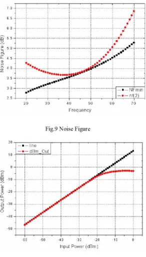
InFig.
9, it
canbe
seenZL
R
+SL
(1)
that the noise
figure is below 4.05dB between
1
3.1GHz to
5.0GHz
and the minimum noise
figure
is
YF
= 1 (2)3.67dB
at3.7GHz.
The
powerconsumption
is
RF
+sLF
+12.5
1mW
through
a1.8V
powersupply.
InFig.
10,
SCF
the
input-referred
1dB
compression
point
(IP1dB)
is
-19dBm
at4.5GHz
and the
11P3
is -5dBm with
ZF
3960MHz
and3970MHz
which is inFig.
11.
V AV iz1 72 VI. CONCLUSION
A
CMOS
UWBLNA
is
designed
for
dual-Fig.3 Miller's Theory mode, MB-OFDM and DS-UWB, radio systems.
The
post-layout
simulation results show that the
proposed
LNA
gives
13.65dB maximum
powergain
between 3.1GHz
to5.0GHz
while
consuming
12.51mW
though
a1.8V
powersupply.
o--- ---d--dBS (1,1 -20--30 *U.. * 5 t 0 ,0 0 i 30
;
NFmin --40 3tt -0-20~ ~ ~50 60~ ~40 ~3070nf2~ ~ S FrequencyFig.6Input Return Loss
Fig.9NoiseFigure
_5-- -M 2 --- ---40---lO-22 32 42 52 60 T: Input2PdBmrOut 14--1 .2- - 30der -14
--2423G 4G 5G 62 6 0 40 30 -1020 020 30 4050~~~~~Frqunc 60 70 Inpu Power(dBm
Frequency Irequency
Fig67IOuputReturn Loss Fg1 nu oe opeso d
40-Fig.8 PowerGain Fig.IIP3~~~~ordel l
20
2-n-iner
12 a U, 0 ~~~~~~~~~~~~~-*-IdBmne u -- - --6l --60--0 -4 -0 -430 -20 -20 -10Frequency ~~~~~~~~~~~~~~~~~InputPower(dBmn)
Fig7
8upu
PoetrGan Figli.OnutPoe 11mp3esonIdACKNOWLEDGEMENT
The authors would like to thank the
chip
implementation
center(CIC)
for technicalsupport.
REFERENCES
i 3i1 [1] FCC, 'Final Rule of the Federal Communications
Commission, 47 CFR Part 15,Sec. 503", Federal Register,
Vol.67,no.95,May2002.
[2]http/ww.ieee8O2.or / /u G3a.htrnl
[3]AndreaBevilacqua,and Ali M.Niknejad,"AnUltrawideband CMOS Low-Noise Amplifier for 3.1-10.6-GHz Wireless Receivers "IEEE JOURNAL OF SOLID-STATE CIRCUITS, Vol.39, No. 12,pp.2259-2268,Dec 2004.
[4]Chang-WanKim,Min-SukKang,Phan TuanAnh,Hoon-Tae
Kim,and Sang-Gug Lee,"An Ultra-Wideband CMOS Low
__>_ _
~~~~~~~~~
Noise Amplifier for 3-5-GHz UWB System", IEEE JOURNAL OF SOLID-STATE CIRCUITS, Vol. 40, No. Fig. 11 Layoutof the PurposedUWBLNA 2,pp.544-547,Feb. 2005.[5] Chang, C.-P.; Chuang, H.-R., '0.18 um 3-6 GHz CMOS broadband LNA for UWB radio", Electronics Letters,
3.1-5.0GHz Volume41,Issue12,June 2005Page(s):33-34.
SII(dB) <-10.10 [6] Zhe-Yang Huang; Chun-Chieh Chen; Che-Cheng Huang;
S22(dB) -9.76 Nan-Ku Lu "Design of CMOS Low-Noise Amplifier for
| S22 (dB) | < -9.76 | Low-Band Ultra-Wideband System" MicrowaveConference
S21(dB) 12.60-13.65 Proceedings, 2005. APMC 2005.Asia-Pacific Conference
S21 Max.(dB) 13.65 Proceedings,Volume5,04-07 Dec.2005Page(s):1-4.
Working Bandwidth(GHz) 3.1-5.0 3dB Bandwidth (GHz) 2.5-6.0 NF(dB) 3.67-4.05 PIdB (dBm) -19 IIP3(dBm) -5 PowerConsumption(mW) j 12.51 Table. 1 Performance Conclusions
Paper CircuitTopology Technology 51I1(dB) S22(dB) SS21(dB) BW(GHz) Gmax(dB) NF(dB) NFmin(dB) Pdiss(mW)
[4] resistivefeedback 0.18umCMOS <-9 <-10 6.8-9.8 2.0-4.6 9.8 2.3-5.2 2.3 12.6
[5] 3-stagescomm.-source 0.18umCMOS <-12.2 <-10.1 13.5-15.8 3.0-6.0 15.7 4.7-6.7 4.7 59.4
[6] 2-stageshunt-peaked 0.18umCMOS <-9.5 <-8.1 15.3-18.0 3.1-5.0 18.03 2.7-3.1 2.7 25.9 This work 2-stagesshunt-peaked 0.18umCMOS <-8.7 <-9.3 111.2-13.1 2.8-6.3 13.1 3.7-5.0 3.7 12.5
Table.2 PerformanceComparisons