面射型雷射高頻特性之研究
100
0
0
全文
(2) 面射型雷射高頻特性之研究 High speed characteristics of Vertical-Cavity Surface-Emitting Laser. 研 究 生:張亞銜. Student:Ya-Hsien Chang. 指導教授:王興宗 博士. Advisor:Dr. Shing-Chung Wang. 郭浩中 博士. Dr. Hao-Chung Kuo. 國 立 交 通 大 學 電機資訊學院 光電工程研究所 博 士 論 文. A Thesis Submitted to Institute of Electro-Optical Engineering College of Electrical Engineering and Computer Science National Chiao Tung University in partial Fulfillment of the Requirements for the Degree of Doctor of Philosophy in. Electro-Optical Engineering July 2005 Hsinchu, Taiwan, Republic of China. 中華民國九十四年七月.
(3) 面射型雷射高頻特性之研究. 研究生:張亞銜. 指導教授:王興宗 教授 郭浩中 教授 國立交通大學光電工程研究所 摘要. 本論文旨在探討面射型雷射高頻特性的改進之道。從雷射發光層的材料、元件結構 與元件等效的寄生電阻電容來改進面射型雷射的高頻操作特性,包跨小信號頻寬與眼 圖。本論文第一部份為使用InGaAsP/InGaP為雷射增益層的面射型雷射。InGaAsP/InGaP 材料的最佳化可藉由光激輝光光譜與理論模擬來達到,理論證明此種量子井具有較大的 光增益與較低的透明電流。元件部分其臨界電流與微分效率分別為 0.4 mA與 0.6 W/A, 相較於傳統的GaAs/AlGaAs量子井,InGaAsP/InGaP具有較高的熱穩定度,當基板溫度從 室溫升高到 85oC時,其臨界電流僅僅升高了 0.2 mA。其小信號頻寬可達 14.5 GHz 而電 流調制效率為 11.6 GHz/(mA)1/2,我們同時展示了 12.5 Gb/s的眼圖,證明了InGaAsP/InGaP 極適合作為高速面射型雷射的主動層。論文的第二部份則聚焦在如何降低在元件的等效 電容。我們使用離子佈植(H+)方法成功阻斷了元件的特性電容使小信號頻寬由 2.3 GHz增 加到 9 GHz,其 10 Gb/s的眼圖也大幅改善,可通過 802.3ae所規範的遮罩。為了精確得知 元件在離子佈植前後的電容與阻抗,我們建立了面射型雷射的等效電路,使用Agilent ADS 軟體從元件量測到的阻抗係數(S11)抽取元件的接面電容,結果證明離子佈植技術能有效 降低雷射寄生電容。論文的最後部分,我們使用漸變氧化層來取代傳統單一組成氧化層, 以做為面射型雷射的電流侷限與光學侷限。漸變氧化層可提供漸變的折射率分佈,理論 上可以減少元件的高頻操作時的阻泥係數。我們發現使用漸變氧化層的面射型雷射具有 相似的靜態特性(LIV),但是其小信號頻寬則由 10 GHz增加到 13.2 GHz,阻泥係數也降 低了一倍,顯示漸變氧化層的確可以改善雷射的高頻響應。. i.
(4) High speed characteristics of Vertical-Cavity Surface-Emitting Laser Student : Ya-Hsien Chang. Advisor : Dr. Shing-Chung Wang Dr. Hao-Chung Kuo. Institute of Electro-Optical Engineering National Chiao Tung University. Abstract The dissertation explores the improvement of high speed performance of vertical-cavity surface-emitting lasers (VCSELs) by adapting new active region, epi-structure, and fabrication process. This dissertation can be divided into three parts. In the first part, we present InGaAsP/InGaP strain-compensated MQWs VCSELs. The InGaAsP/InGaP MQWs composition was optimized through theoretical calculations and the growth condition was optimized using photoluminescence. These VCSELs exhibited superior performance with characteristics threshold currents ~0.4 mA, and the slope efficiencies ~ 0.6 mW/mA. The threshold current change with temperature is less than 0.2 mA and the slope efficiency drops less than ~30% when the substrate temperature is raised from room temperature to 85oC. High modulation bandwidth of 14.5 GHz and modulation current efficiency factor of 11.6 GHz/(mA)1/2 are demonstrated. In the part two of this thesis, we investigate high speed performance of oxide-confined VCSELs with planar process and reduced parasitic capacitance by proton implantation. The parasitic capacitance of VCSELs was reduced using additional proton implantation. The small signal modulation bandwidth which was restricted by electrical parasitic capacitance expanded from 2.3 GHz to 9 GHz after proton implantation. To investigate the extrinsic bandwidth limitation of the oxide VCSELs, an equivalent circuit for the VCSEL impedance was introduced. The reflection coefficient showed that the electric parasitic pole exceeded 20 GHz. The eye diagram of VCSEL with reduced parasitic capacitance operating at 10Gps with 6mA bias and 6dB extinction ratio showed a very clean eye with a jitter of less than 20 ps. This simple method can be applied to mass production with low cost. In the last part, we present the improved oxide-implanted VCSELs utilizing the tapered oxide layer. The VCSELs exhibited similar static performance, but superior modulation bandwidth up to 13.2 GHz, compared with conventional blunt oxide VCSELs. The damping rate was reduced two times in the tapered oxide VCSEL and ii.
(5) therefore enhanced the maximal modulation bandwidth. A very clean eye was demonstrated from improved VCSEL with rising time of 26 ps, falling time of 40 ps and jitter of less than 20 ps, operating at 10Gb/s with 6mA bias and 6dB extinction ratio.. iii.
(6) 誌謝 博士班的生涯,充滿驚異,畢業在即,心中充滿感謝。 首先,最要感謝指導老師郭浩中教授,在研究上的指導與教誨,使我學習到 歸劃與執行整體研究的方法,讓我受益良多,也更認識自己的長處與短處,對我 的人生有著很深的影響。謝謝指導老師王興宗教授的耐心,包容我的無知莽撞與 粗心。 這些年來,感謝與我共同奮鬥,一起成長的學弟妹,毅彬、峻瑋、俊毅、妙 佳、俊麟、國峰、敏瑛,我們完成過許多挑戰性的任務,謝謝你們。感謝老同學 蔡睿彥、姚忻宏在學習過程互相勉勵,特別是和我一起在實驗室努力討生活的賴 芳儀、薛道鴻,多年互相支持鼓舞,大家都辛苦了。 實驗研究過程中,要感謝工研院宋嘉斌博士、楊泓斌博士在雷射製作與設計 上幫忙;感謝成大尤信介博士驗上的支援,給予我很多的幫忙及生活上的關心; 感謝工研院媽媽桑、嬸嬸、阿月對我的照顧。陳智弘老師在實驗上的指導建議與 討論。感謝博士後賴利弘學長、林佳鋒學長的協助,謝謝你們。 感謝碩士時期白世璽學長的教導,給予我生涯規劃的意見與支持。感謝博士 班學長老余對我的照顧與建議,初聞你結婚的消息,讓我再次體認造物主的奇 妙,你讓我瞭解到再怎麼樣的傳奇人物也有安定下來的一刻。感謝李兆逵學長在 資料收集與建檔的細心與系統化備份,大大地增長了我的視野。博士班學弟志 強、泓文、榮堂,你們的低級笑話,大大抒解了研究與實驗的壓力,我知道你們 會繼續下去的。鴻儒學長,你的鼓勵一直是我堅持下來的動力,謝謝你給予我生 涯規劃的建議與支持。怡安,謝謝你在模擬上的協助。宗憲、德忠與你們合作十 分愉快。感謝碩士班學弟妹哲偉、文君、永龍、威佑、偉倫,你們撇下我早早畢 業,曾經讓我很不爽,現在我都原諒你們了!薏婷,謝謝你協助處理很多實驗室 的事務與提供重要資料的下載。文燈、傳煜、裕鈞,祝你們一帆風順。謝謝實驗 室助理淑致、麗君在行政上的幫忙。感謝所辦黃小姐、湯先生、許小姐、劉小姐、. iv.
(7) 崔小姐等在計畫及行政作業上的幫忙。文凱、游敏與意偵,祝你們實驗順利!柏 傑,希望還有機會一起打球!感謝所有曾經幫助過我的老師以及朋友們。此外, 玉珠,謝謝你兩年來的陪伴。 最後,特別要感謝我的家人給我最溫馨的支持與關懷以及無怨無悔的付出, 媽媽、祐榮、翔宸,謝謝你們。僅將此論文獻給他們以及我所最親愛的母親。 謝謝大家! 亞銜. 于 94 年 7 月 27 日. 交通大學光電工程研究所. v.
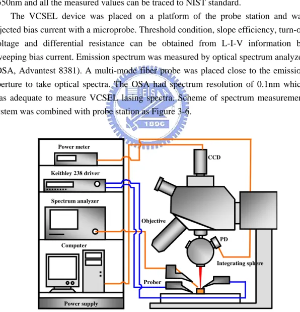
(8) Content Abstract ( in Chinese )………………………………..….………………………………i Abstract ( in English ) …………….……………….…..…………………………...…...ii Acknowledgment……………………………………………...……………………...…..iv Contents……………………………………………………………………………...........vi Figure Captions………………………………………………...……………….............viii Table Captions…………………………………………………..………………….…...xi. CHAPTER 1. Introduction 1.1 Structure of VCSELs………………………………………..…………………..…..1 1.2 Material for active Region…………………………………………………………..3 1.3 Advantages of VCSELs……………………………………………………………..4 1.4 Drawback of VCSELs……………………….……………………………………....5 1.5 Applications 1.5.1. Data communication………………………………………………………6. 1.5.2. Optical interconnect…………..………………………………………..….7. 1.5.3 Sensor……………………………………………………………….......... 7. CHAPTER 2. Rate Equations and laser dynamics 2.1 Carrier Rate equation…………………………………...………………………….12 2.2 Small signal modulation………………………………...…………………………24 2.3 Relative intensity noise……………….…………...….……………………………27. CHAPTER 3. Experimental Setup 3.1 Inductively coupled plasma reactive ion etching…………………………………..28 3.2 Ion implantation system……………………………………………………………30 3.3 Oxidation process…………………………………………………..…………….33 3.4 Probe station and spectrum measurement system…………………………………35 3.5 Far-Field and Near-Field…………………………………………………………...35 3.6 Microwave test system……………………………………………………………..36 vi.
(9) 3.7 Relative Intensity Noise measurement.……...………………….………………….39. CHAPTER 4. Strain-Compensated InGaAsP/InGaP MQWs VCSELs 4.1 Theory……………………………………………………………………………...41 4.2 Fabrication Process of polyimide planarized VCSEL……………………………..42 4.3 Result and Discussion…………………………………..……………………..…43 References……………………………………………………………………………...45. CHAPTER 5. Reducing capacitance of Oxide-Confind VCSEL by proton implantation 5.1 Introduction…………………………………………….……………………..……56 5.2 Fabrication Process………………………………….……………………………..56 5.3 LIV / 3-dB Bandwidth / Eye diagram……………..………….………....................57 5.4 Equivalent circuit extraction……………………………………….………………58 References…………………………………………………………….……………….59. CHAPTER 6. Tapered oxide VCSELs 6.1 Review of tapered oxide layer…………………………………………….……….66 6.2 Sample structure and fabrication process………………………………….………67 6.3 LIV performance and small signal response……………………………….………67 6.4 Eye diagram of tapered oxide VCSEL…………………….……………………….69 References…………………………………………………….……………………….70. CHAPTER 7. Summary……….…………………….……………..……………….....79 Curriculum Vita…………………………………………………………………………82. Publication List………………………………………………………….………………83. vii.
(10) List of Figures. Figure 1-1 Structure of vertical-cavity surface-emitting laser Figure 1-2 Comparison of edge emitting laser and vertical-cavity surface-emitting laser Figure 1-3 Material for vertical-cavity surface-emitting laser in wide spectra band Figure 1-4 Commercial 2.5 Gb/s VCSEL array for data communication application. Figure 1-5 A laser mouse module using VCSEL. Figure 2-1 The individual terms considered by general carrier rate equation. Figure 2-2 The continuous pumping is the essential condition to reach population inversion. Figure 2-3 Stimulated absorption generates more electron-hole pairs. Stimulated emission produced coherent light (same energy, phase, propagation direction, highly monochromatic). Figure 2-4 The interaction of stimulated absorption and stimulated emission contribute the optical gain of material. The “gain” represents in this figure is just the ratio of photons that is not the same as “material gain” we will discuss later. It also presents the gain is the function of photons traveling length. Figure 2-5 The material gain (G) is as function of carrier concentration (N). Figure 2-6 Spontaneous recombination emits incoherent light in all directions which is a random process. Figure 2-7 Comparing spectra for spontaneous and stimulated emission. Figure 2-8 Two non-radiative recombination mechanisms. Figure 2-9 The individual terms considered by general photon rate equation. Figure 3-1 Cross section structure of tapered oxide implant VCSEL structure Figure 3-2 Steps of oxide-implant VCSEL process Figure 3-3 Illustration of oxidation process system setup Figure 3-4 Oxidation rate of 98% Al-content layer. viii.
(11) Figure 3-5 (a) Cross section structure of oxide photonic crystal VCSEL structure (b) top view image of the PC-VCSEL;(c) scanning electron microscope image of an etched hole. Figure 3-6 Steps of oxide photonic crystal VCSEL process Figure 3-7 Cross section structure of implant photonic crystal VCSEL Figure 3-8 Probe station measurement instrument setup Figure 3-9 Far field pattern measurement system Figure 3-10 Eye diagram measurement instrument setup Figure 4-1 Schematic energy bandgap diagram for In0.18Ga0.82As0.8P0.2/In0.4Ga0.6P active region. Figure 4-2 Material gain spectrum and material gain as a function of carrier density of In0.18Ga0.82As0.8P0.2/In0.4Ga0.6P MQW and GaAs/Al0.26Ga0.74As MQW Figure 4-3 (a) Schematic cross section of high speed VCSEL structure (b) Process steps of high speed VCSELs. Figure 4-4 PL spectra of SC-MQW with different growth interruption times. Figure 4-5 SEM picture of the finished VCSEL Figure 4-6 SC-MQWs InGaAsP/InGaP VCSEL light output and voltage versus current (LIV) curves at room temperature and 85°C. Figure 4-7 Optical spectrum at 6 mA of the VCSEL Figure 4-8 Small-signal modulation responses of a 5 µm diameter VCSEL at different bias current levels. Figure 4-9 Resonant frequency as a function of square root of current above threshold current. Figure 4-10 (a) 25°C (b) 85°C eye diagram of SC-VCSEL up to 12.5 Gb/s with 6dB extinction ratio. The scale in the fig. is 15 ps/div. Figure 4-11 HTOL (70oC/8mA) performance of strain compensated VCSEL.. ix.
(12) Figure 5-1 L-I-V curves of three oxide-implanted VCSELs (solid lines) and three oxide-only VCSELs (dashed lines). Figure 5-2 Small signal modulation response of (a) oxide-only VCSEL (b) oxide-implanted VCSEL Figure 5-3 Resonant frequency and 3 dB frequency for oxide-only VCSELs (square symbol) and oxide-implanted VCSELs (circle symbol) Figure 5-4 Eye diagram of (a) oxide-only VCSEL (b) oxide-implanted VCSEL Figure 5-5 Reflection coefficient (S11) for oxide-only device (dashed line) and oxide-implanted device (solid line) at 3 mA Figure 5-6 Equivalent circuit used for the oxide confined VCSEL impedance Figure 6-1 L-I-V curves of the tapered oxide VCSELs (solid lines) and the blunt oxide VCSELs (dashed lines). Inset is top view image of the VCSEL. Figure 6-2 Small signal modulation response of (a) the tapered oxide VCSEL and (b) the blunt oxide VCSEL. Figure 6-3 3-dB frequency of the oxide-implanted VCSELs as a function of root square of bias current above threshold. (Filled square: tapered oxide VCSELs, Opened square: blunt oxide VCSELs) Figure 6-4 Damping rate as a function of resonance frequency squared for VCSELs. (Filled square: tapered oxide VCSELs, Opened square: blunt oxide VCSELs) Figure 6-5 Real and Imaginary part of S11 parameter versus frequency from model and measured data. Inset is the equivalent circuit model of VCSELs. Figure 6-6 Eye diagram of the tapered oxide VCSELs at PRBS of 231-1 and 6dB extinction ratio, biased at 6 mA. (the time scale is 15.6 ps/div). x.
(13) List of Tables. Table 1-1 Comparison of parameters between stripe laser and VCSEL Table 6-1 Extracted circuit values at different bias current for the tapered oxide VCSELs. xi.
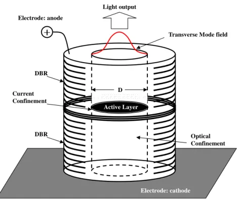
(14) CHAPTER 1. Introduction. The surface-emitting laser is considered as one of the most important devices for short range optical communication, storage area network, and optical interconnects. In this chapter, we briefly review the history and introduce the concept of vertical-cavity surface-emitting laser from the structure of VCSELs and compare it with conventional edge emitting lasers(EEL). Then, we will discuss some important applications and future prospects. The vertical-cavity surface-emitting laser was first proposed by Iga et. al. in 1979 [1], demonstrated under pulsed conditions at room temperature (RT) by the same group five years later[2], and finally continuous wave (CW) operation at room temperature was achieved in 1989 [3]. The achievements encouraged people to devote into the development of the VCSELs with different structure and novel materials. After that, VCSELs based on GaAs have been extensively studied and devices in 980, 850, and 650 nm are now commercial available. The research of InGaAsN, a key material toward 1300nm on GaAs substrate nowadays, started in mid-90 and is still improving up to now.. 1.1 Structure of VCSELs As its name indicates, the fundamental difference between an edge-emitting laser and a vertical cavity surface emitting laser is the fact that the laser oscillation as well as the out-coupling of the laser beam occur in a direction perpendicular to the epitaxial gain region and the surface of the laser chip. The structure of most VCSELs consists of two parallel reflectors which sandwich a thin active layer, is illustrated with Figure 1-1. The reflectivity necessary to reach the lasing threshold should normally be higher than 99.5%. Together with the optical cavity formation, the scheme for injecting electrons and holes effectively into the small volume of the active region is necessary for a current injection device. The ultimate threshold current depends on how to small the active volume can be make and how well the optical field can be confined in the cavity to maximize the overlap with the active region. These confinement structures will be presented later.. 1.
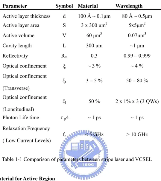
(15) Light output Electrode: anode Transverse Mode field. DBR D. Current Confinement. Active Layer. DBR. Optical Confinement. Electrode: cathode. Fig. 1-1 Structure of vertical-cavity surface-emitting laser Figure 1-1 A modal of vertical cavity surface emitting laser (VCSEL). Figure 1-2 illustrates the typical differences edge-emitting laser and VCSELs. The overall cavity length is much shorter for a VCSEL, typically a few um, as opposed to some mode spacing and shorter gain region. In order to compensate for the shorter gain region, the light has to travel back and forth more times before coupled out, therefore the mirror reflectivity have to be much higher. The reflectivity of an output facet for an edge emitting laser, resulting from the change of refractive index at the cleaved interface semiconductor-air is typically around 30%. The structure parameters are listed in Table 1-1. and compared with the edge emitting lasers.. Fig. 1-2 Comparison of edge emitting laser and vertical-cavity surface-emitting laser 2.
(16) Parameter. Symbol Material. Wavelength. Active layer thickness. d. 100 Ǻ ~ 0.1µm. 80 Ǻ ~ 0.5µm. Active layer area. S. 3 x 300 µm2. 5x5µm2. Active volume. V. 60 µm3. 0.07µm3. Cavity length. L. 300 µm. ~1 µm. Reflectivity. Rm. 0.3. 0.99 – 0.999. ξ. ~3%. ~4%. ξt. 3–5%. 50 – 80 %. ξl. 50 %. 2 x 1% x 3 (3 QWs). τ p4. ~ 1 ps. ~ 1 ps. fr. < 5 GHz. > 10 GHz. Optical confinement Optical confinement (Transverse) Optical confinement (Longitudinal) Photon Life time Relaxation Frequency ( Low Current Levels). Table 1-1 Comparison of parameters between stripe laser and VCSEL. 1.2 Material for Active Region There are some choices of the materials for semiconductor lasers in Figure 1-3. The Wavelength (µm). 0.3. 0.5. 0.8. 1.0. 1.3. GaInAsP/InP AlGaInAs/InP. 1.3~1.6 1.2~1.3. GaInNAs/GaAs 0.78~0.88. GaInAs/GaAs 0.78~0.88. GaAlAs/GaAs. 0.63~0.67. GaAlInP/GaAs ZnSSe/ZnMgSSe GalnAlN/GaAlN. 1.5. 0.45~0.55 0.3~0.5. Figure 1-2for Material for VCSELssurface-emitting in wide spectral bands Fig. 1-3 Material vertical-cavity laser in wide spectra band. 3.
(17) availability of substrates against lattice constant related to the systems is also shown. The problems are listed below that should be taken into account consideration for making VCSELs: ▲ Design of resonant cavity and mode-gain matching ▲ Multi-layered distributed Bragg reflectors (DBRs) to realize high-reflective mirrors ▲ Heat sinking for high temperature and high power operation In addition, the resistivity of material is crucial for high speed operation. So far, these are mainly two methods of current confinement schemes for the VCSEL structures, ▲ Proton-implant type: An insulating layer made by proton (H+) irradiation to limit the current spreading toward the surrounding area. The progress is rather simple and most commercialized devices are made by this method. ▲ Selective AlAs oxidation type: By oxidizing the AlAs layer to form an insulator.. 1.3 Advantages of VCSELs There are many reasons why VCSELs are becoming increasing popular as light source for applications such as datacomm and optical interconnects. The monolithically integrated structure requires one single epitaxial run, making it easier to fabricate. Since the mirrors are formed during the epitaxial growth, each individual VCSEL can be tested already on the wafer, before it is cleaved into separate chips, thereby drastically reduce the production cost. The use of DBRs eliminates the risk of catastrophic optical damage (COD) in the mirrors which can occur in edge-emitters where the active material close to the facets are depleted by surface recombination and thereby light absorbing. It also reduces the risk of mechanical mirror damage. The extremely short resonator leads to a large longitudinal mode spacing that is large compared with the gain bandwidth and leads to inherent single longitudinal mode operation. The small active volume and high mirror reflectivity contribute to the very low threshold observed in VCSELs, as low as a few microamperes[4], resulting in low power 4.
(18) consumption and reduced heating of the device. This feature, combined with the absence of CODs, explains the remarkable reliability of VCSELs. Lifetimes of more than 10000 hours have been reported by several groups. [5-6] The surface emission and the small size make it possible to fabricate very dense two-dimensional arrays of VCSELs, suitable for multi-channels parallel transmission modules. [7] VCSELs do not need to be cleaved; it is therefore possible to integrate them monolithically with other optoelectronic components such as photodetectors, modulator or hetero-bipolar transistors (HBT). [8] Because of the circular symmetry of the VCSEL structure, the light is emitted with a circular beam and very low divergence. This results in high coupling into optical fibers, up to 90% [9] and allows for relaxed tolerance in alignment, further reducing the cost of installation. For comparison, the output light emitted from an edge-emitting laser is elliptical with a transverse and lateral divergence of about 40 and 10 degrees, respectively, making it cumbersome to couple the light into an optical fiber without significant optical loss or advanced optics. In addition, VCSELs have inherent single-wavelength structure that is well suited for wavelength engineering, making it possible to process multi-wavelength array or tuneable VCSELs. Although the manufacturing challenges are numerous, both types of devices have been demonstrated. By carefully designing the optical cavity, with the implemenatation of a small thickness variation in the bottom DBR, a record 150-wavelength VCSEL array has been reported. The thickness gradient creating a cavity thickness variation, which in turn led to laser wavelength variation, the overall wavelength span across the array being 43 nm. [10]. 1.4 Drawbacks of VCSELs However, VCSELS also have some drawbacks compared to edge-emitters. The manufacturing tolerances on VCSEL growth are much tighter than for edge-emitting lasers, the layer thickness having to be controlled within 1%. The major disadvantage with VCSELs is the strong tendency to operate on multiple transverse modes, due to the large transverse dimensions of the optical cavity. These results in emission spectra with multiple emission wavelengths, which limits the maximum achievable distance due to chromatic dispersion effects. Most commercial VCSEL of today operate multimode and are mainly used in short distance multimode fiber based optical data links[11], optical interconnects[12], optical storage[13] and laser printing[14]. A lot of efforts are made to produce high power single mode VCSELs. This include oxide confined VCSELs with current aperture small enough to support only the fundamental mode, index-guided structures such as regrown or surface relief 5.
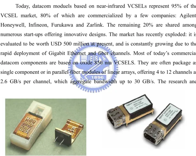
(19) VCSELs, and spatial mode filtering in an external cavity or extended cavity. Although the first and last of these techniques have produced high single mode power they are difficult to implement with high uniformity and yield. A more reliable technique is to combine a large area oxidation with an etched shallow surface relief for mode selection. This implies only a small modification to the fabrication procedure but produces reasonably high single mode power, with high uniformity and yield. [15]. 1.5 Applications of VCSELs. 1.5.1 Data communication Today, datacom moduels based on near-infrared VCSELs represent 95% of the VCSEL market, 80% of which are commercialized by a few companies: Agilent, Honeywell, Infineon, Furukawa and Zarlink. The remaining 20% are shared among numerous start-ups offering innovative designs. The market has recently exploded: it is evaluated to be worth USD 500 million at present, and is constantly growing due to the rapid deployment of Gigabit Ethernet and fiber channels. Most of today’s commercial datacom components are based on oxide 850 nm VCSELS. They are often package as single component or in parallel fiber modules of linear arrays, offering 4 to 12 channels at 2.6 GB/s per channel, which aggregate bandwidth up to 30 GB/s. The research and. Fig. 1-4 Commercial 2.5 Gb/s VCSEL array for data communication application. development efforts are focusing on the next generation of high speed VCSEL, and a number of groups have reported transmission at 10 GB/s or more for distances up to 300 m of MMF.. Figure 1-4 shows a 12 channel 2.5 Gb/s VCSEL array for short distance. transmission applications. For long wavelength part, Metro and Access Networks are dominated by 1300nm 6.
(20) and 1550 nm FP and DFB lsers up to now. A long wavelength VCSEL (LW-VCSEL) would be an ideal low-cost alternative to the DFB laser, particularly for the standard IEEE 802.3ae applications, which extend the existing Gigabit Ethernet into traditional SONET markets at OC-192 data rates.[16]. However, the performance specifications for such LW-VCSELs are challenging. For low-cost transceivers, they must operate over the 0 to 70 C temperature range for indoor applications and over the -40 to 85 C range for outdoor applications, without external temperature stabilization. The laser power launched into the single mode fiber must usually be more than 0.7 mW in order to support transmission distance of 10 km at 10 GB/s. Despite intense research effort, the technology so far has not yet met these requirements. 1.5.2 Optical interconnect The optical interconnect is considered by many to be inevitable in the computer technology. The performance of massively parallel computers is usually limited by the communication bottleneck between processors. Optic provides an effective mean to line these processors because of its high capacity, low crosstalk and attenuation, and the possibility to obtain three-dimensional architectures. Other potential applications include routers, switches and storage. The VCSEL is a strong candidate as the preferred optical light source for the emerging optical interconnect mass market, meeting the requirement of low cost, high density integration and low power dissipation. A 256-channel bi-directional optical interconnect using VCSELs and photodiodes on CMOS was demonstrated.[17]. 1.5.3 Sensor Reflective optical sensors are used to sense the presence or absence of a distant object. Examples of reflective sensors used in a variety of industrial and consumer products include barcode scanners and proximity sensors. The packaging of optical reflective sensors can be quite compact, and in the case of some LED sources, can even be packaged in a single TO can. However, a significant disadvantage to these devices is the quantity of optical crosstalk that may degrade the signal-to-noise ratio (S/N) in the detector. Crosstalk results from the fact that LEDs emit from all surfaces and the emission subtends nearly 90°. Suppliers go to great lengths to isolate the LED and the detector by using a mechanical structure to separate the optoelectronic components. In addition, the LED optical output is not easily collimated or focused to a spot to increase the amount of reflected light from a distant object. By using the technical features of the VCSEL, integrating a phototransistor in the package, and designing 7.
(21) the optical element into the TO can lid, an effective reflective sensor can be developed. The advantages of the sensor include the ability to package the entire assembly in a single compact TO can, along with the focusing optics and a phototransistor. Depending on the application, a single-mode or multimode VCSEL can be used. In some cases, when coherence of the optical beam is desired, the single-mode VCSEL might be the best choice, but in other cases when total output power is more important, a multimode VCSEL might be more beneficial. For example, a multimode VCSEL can be mounted on the centerline of the lens and package, and the phototransistor mounted to the side of the VCSEL. In this configuration, the optimal signal is obtained by tilting the package with respect to the centerline of the TO. The optical system is made by including a melt-formed glass lens in the TO lid. The lid can be designed to accept other lenses, and the height can be varied, which allows for the design of a wide variety of optical sensors. In addition to the reduced power consumption and single-package interface, the recurring theme in the application is the ability of the VCSEL sensor to provide higher S/N in environments where the LED sensor is not able to adequately perform. Other application areas include the sensing of diffuse reflective surfaces such as paper in a printing system, or low-reflectivity surfaces such as glasses or plastics. The small focal spot also has significant advantages in optical encoding applications such as barcode. VCSEL. Fig. 1-5. A laser mouse module using VCSEL.. reading or positioning equipment. Figure 1-5 illustrate the VCSEL sensor module used in laser mouse application. The sensitivity and resolution of the laser mouse is 20 times higher than the conventional LED mouse. In 2004, the VCSEL based biosensor also demonstrated by C. J. Chang-Hasnain et al. [18-19]. 8.
(22) References [1]. H. Soda, K. Iga and Y. Suematsu, “GaInAs/InP surface emitting injection lasers”, Jpn. J. Appl. Phys. v.18, 2329, (1979). [2] K. Iga, Sishikawa, S. Ohkouchi and T. Nishimura, “Room temperature pulsed oscillation of GaAlAs/GaAs surface-emitting injection laser”, App. Phys. Lett. v45, 348, (1984) [3] F. Koyama, S. Kinoshita and K. Iga, “Room-temperature continuous wave lasing characteristics of GaAs vertical cavity surface-emitting lasers”, App. Phys. Lett. V44, 221, (1989) [4] G. M. Yang, M. H. MacDougal and P. D. Dapkus, “Ultralow threshold current vertical-cavity surface-emitting lasers obtained with slelective oxidation”, Electron. Lett., Vol. 13. pp. 886-888, 1995 [5] J. K. Guenter, J. A. Tantum, A. Clark. R. S. Penner, R. H. Johnson, R. A. Hawthorne, J. R. Biard, Y. Liu, “Commericalisation of Honeywell’s VCSEL technology:further developments”, Proceedings of SPIE’s Optoelectronics 2001, Vol. 4286, pp. 1-14, 2001. [6] J. S. Span, Y. S. Lin, C. F. Li, C. H. Chang, J. C. Wu, B. L. Lee, Y. H. Chuang, S. L. Tu, C. C. Wu, “Commericailised VCSEL components fabricated at Truelight Corporation”, Proceedings of SPIE’s Optoelectronics 2001, Vol. 4286, pp. 15-21, 2001. [7] A. V. Krishnamoorthy, K. W. goossen, L. M. F. Chirovsky, R. G. Rozier, P. Chandramani, S. P. Hui, J. Lopata, J. A. Walker, L. A. D’Asaro, “16x16 VCSEL array flip-chip bonded to CMOS VLSI circuit”, IEEE Photon. Technol. Lett., Vol. 12, pp. 1073-1075, 2000 [8] U. Eriksson, P. Evaldsson and K. Streubel. “A novel technology for monolithic integration of VCSELs and heterojunction bipolar transistors at 1.55um”, CLEO Pacific Rim ’97, Chiba, Japan, paper PD2.8, 1997 [9] K. Tai, G. Hasnain, J. D. wyn, R. J. Fisher, Y. H. Hang, B. Weir, J. Gamelin and A. Y. Cho, “90% coupling of top surface-emitting GaAs/AlGaAs quantum well laser output into 8 um diameter core silica fiber”, Electron. Lett., Vol. 26, pp. 1628-1629, 1990 [10] M. Y. Li, W. Yuen, G. S. Li and C. J. Chuang-Hasnain, “Top-emitting micromechanical VCSEL with a 31.6nm tuning range”, IEEE Photon. Technol. Lett., Vol. 10, pp. 18-20, 1998 [11] U. Fiedler, G. Reiner, P. Schnitzer and K. J. Ebeling, “Top surface-emitting vertical-cavity laser diode for 10GB/s data transmission”, IEEE Photon. Technol. Lett., Vol. 8, pp. 746-748, 1996 [12] M. W. Haney, M. P. Christensen, P. Milojkovie, J. Ekman, P. Chandramani, R. Rozier, F. Kiamilev, Y. Liu and M. Hibbs-Brenner, “Multichip free-space global optical 9.
(23) interconnection demonstration with integrated arrays of vertical-cavity surface-emitting lasers and photodetectors”, Appl. Opt., Vol. 38, pp. 6190-6200, 1999 [13] K. Goto, “Proposal for ultrahigh density optical disk system using a vertical cavity surface emitting laser array”, Jpn. J. Appl. Phys., Vol. 37, pp. 2274-2278, 1998 [14] R. L. Thornton, “Vertical-cavity lasers and their application to laser printing”, Proc. SPIE, Vol. 3003, pp. 112-119, 1997 [15] H. Martinsson, J. A. Vukusic, M. Grabherr, R. Michalzik, R. Jager, K. J. Ebeling and A. Larsson, “Transverse mode selection of large-area oxide-confined vertical-cavity surface-emitting laser using a shallow surface relief”, IEEE Photon. Technol. Lett., Vol. 11, pp. 1536-1538, 1999 [16] http://grouper.iee.org/groups/802/3/ae/index.html [17] D.V. Plant, M. B. Venditti, E. Laprise, J. Faucher, K. Razavi, M. Chateauneuf, A. G. KirK, J. S. Ahearn, “256-channel bi-directional optical interconnect using VCSELs and photodiodes on CMOS”, J. Lightwave Techno. 19(8) 1093, 2001 [18] F. Mateus, M. C. Huang, Univ. of California/Berkeley; P. Li, B. Cunningham, SRU Biosystems; C. J. Chang-Hasnain, “High sensitivity label-free biosensor using VCSEL” , Proceedings of SPIE’s BIOS 2004. vol. 5328-22, 2004.. [19] D. Kumar, H. Shao, Kevin Lear, "Dependence of vertical cavity surface emitting laser diodes with integrated micro-fluidic channels on fluid refractive index" Optical Information systems II in series Proceedings of SPIE, vol. 5557, Aug 2004. 10.
(24) Chapter 2. Rate Equations and laser dynamics. The rate equations provide the most fundamental description of the laser. It describes the time-evolution of carrier- and photon densities in a laser cavity as a function of the pump rate, material gain and parameters associated with the material properties and laser construction. In its simplest form, it consists of a pair of coupled nonlinear differential equations Eq.(2-1), one for the carrier density, and one for the photon density. Therefore it is well suited for modeling simulation. By this technique, many of properties of VCSELs can be investigated in this paper. ⎧ dN (t ) η i I (t ) N (t ) = − ν g S (t )G ( N , S ) − ⎪ qVa τN ⎪ dt ⎪ dS (t ) N (t ) S (t ) = Γν g S (t )G ( N , S ) + β − ⎨ τN τS ⎪ dt ⎪ N (t ) − N tr ⎪G ( N , S ) = g 0 1 + εS (t ) ⎩. (2-1). The phase does not enter into Eq.(2-1), since the optical power does not depend on the phase, it depends on the optical magnitude only. However, some effects are highly related to the laser phase, such as mode locking, injection locking and polarization switching, etc, in this situation, the phase has to be taken into account. Before proceeding further, it is important to clear up the fundamental mechanisms and assumption in the rate equations, such as stimulated and spontaneous emission, stimulated absorption, non-radiative recombination, and so on. When referring to “carriers”, the ambipolar assumption is applied, that means there is no difference between electrons and holes. 2.1 Carrier Rate Equation The rate of change of the electrons (or holes) density comes from electron-hole generation and recombination. And these changes must be related to the number of photons produced (for a direct bandgap semiconductor). We assume that the electrons and holes remained confined to the active region having volumeVa . It is intuitive to obtain the basic form of carrier rate equation:. 11.
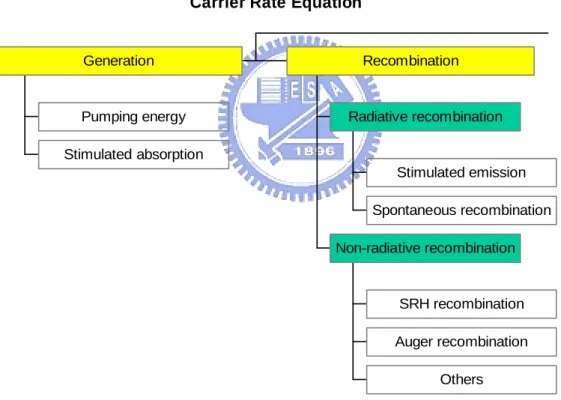
(25) dN = Generation - Recombination dt Stimulated emission ⎞ Non = Pump − ⎛⎜ − Spontaneous recombination − ⎟ radiative recombination ⎝ − Stimulated absorption ⎠ = Ginj − Rstim − Rspon − Rnonr (2-2) where Ginj is pumping energy, Rstim is stimulated recombination which is the difference between stimulated emission and stimulated absorption, Rspon is spontaneous emission, and Rnonr is non-radiative recombination. In Figure 2.1, it shows all the individual terms contribute to the carrier rate equation. Now, we will carefully examine each term as the section proceeds.. Carrier Rate Equation. Generation. Recombination. Pumping energy. Radiative recombination. Stimulated absorption Stimulated emission Spontaneous recombination Non-radiative recombination. SRH recombination Auger recombination Others. Fig 2.1. 2.1.1. The individual terms considered by general carrier rate equation.. Pumping Energy. The pump consists of either bias current or optical flux. The pump term describes the density of electron-hole pairs produced in the active volume Va in each second, which is given by 12.
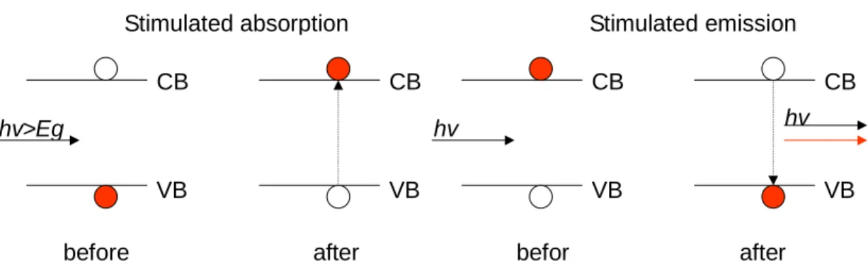
(26) Ginj =. ηi I (t ). (2-3). qVa. where Ginj is pumping current density per second (carriers/cm3/ sec), η i is injection efficiency or internal quantum efficiency (ideal is 1), I (t ) is injection current per second, q is the elementary charge which changes the units from coulombs to the “number of electrons”. Pump increases the number of electrons and holes in the conduction band (CB) and valence band (VB), respectively, is shown in Figure 2.2.. CB. CB. VB before. Fig. 2.2 The continuous pumping is the essential condition to reach population inversion.. VB after. The injection efficiency η i represents the fraction of injected current that flow into the active region. In practical, due to the surface leakage or other carrier loss mechanisms, the η i is always less than 1, it is defined by. ηi ≡. 2.1.2. carriers in active region total injected carriers in the device. (2-4). Stimulated absorption and stimulated emission. The reason we discuss stimulated absorption and emission in the same section is due to their interaction will be used to present the concept of gain medium, it is the major part of laser device ( recall laser = Light Amplified by the Stimulated Emission of Radiation ). Both of stimulated absorption and stimulated emission results from stimulated recombination, therefore, need photons to conduct its process (see Figure 2.3). In contrast, the spontaneous emission does not need photons to conduct its process, will be discussed in next section(2.1.3). According to their various physical mechanisms, please refer to [1][2][3] for further explanation, again, the main purpose of this paper is to demonstrate how to build up a device model based on well-known electro-optics theory. In the simplest way to merge stimulated absorption and recombination mechanisms into to rate equations is to understand the stimulated absorption process would decrease photons number and electron-hole pairs increased. 13.
(27) On the opposite, the stimulated recombination process would multiple increase photons (photons amplified) and electron-hole pairs decreased, that’s why the pumping current should maintain in a certain level to keep the emission process continuously in the active region.. Stimulated absorption CB. Stimulated emission CB. hv>Eg VB after. CB hv. hv VB. before. CB. VB befor. VB after. Fig. 2.3 Stimulated absorption generates more electron-hole pairs. Stimulated emission produced coherent light (same energy, phase, propagation direction, highly monochromatic). The term Rstim is stimulated recombination which is the difference between stimulated emission and stimulated absorption, usually, the stimulated recombination produces more photons than them absorbed (this is one of the essential conditions for lasing, otherwise, the gain will be less than one, no amplified). The Figure 2.4 shows single photon incident on the left side of the gain medium. This photon enters the material and interacts with the carriers. Some of the processes emit photons (stimulated emission) while some of them absorb photons (absorption or sometimes called stimulated absorption) and some do nothing. It implies the gain is the ratio of output photons over the input photons. The gain describes here only the stimulated emission and absorption processes and does not include photon losses through the side of the laser or through the mirrors.. 14.
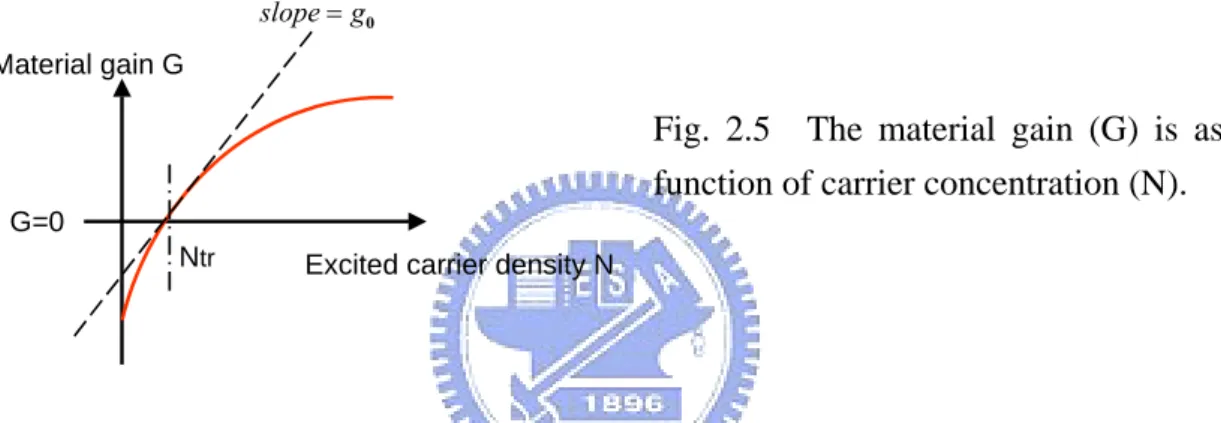
(28) CB hv. hv hv. hv hv hv hv. hv hv hv. gain=4/1=4 (lasing condition). VB CB hv. hv hv. no photon emission. hv. negative gain (no lasing). VB. CB gain=1/1=1 hv. hv hv. hv hv. hv. (transparency condition). VB Fig. 2.4 The interaction of stimulated absorption and stimulated emission contribute the optical gain of material. The “gain” represents in this figure is just the ratio of photons that is not the same as “material gain” we will discuss later. It also presents the gain is the function of photons traveling length. The lower one of Figure 2.4 brings up one terminology, called “material transparency”. The semiconductor material becomes “transparent” (“material transparency”) when the rate of stimulated absorption just equals the rate of stimulated emission. One incident photon produces exactly one photon in the output. The transparency density N tr (number per unit volume) represents the number of excited carriers per volume required to achieve transparency. The material gain required to achieve lasing will be much larger than zero since the gain must offset other losses besides stimulated absorption (typically G=150 cm -1 ). The relation between material gain and carrier density is depicted in Figure 2.5. This yields the simplest expression of material gain: G ( N ) = g0 ( N − N tr ) (2-5). 15.
(29) where g 0 is linear gain coefficient or differential gain at N tr , N tr is transparency density. In this case, we assume the photon density S is not high. Therefore, the gain curves can be approximated by a straight line at N tr (refer to Figure 2.5). When photon density is high enough, the factor (1 + εS ) is taken into account. This factor accounts for nonlinear gain saturation, where ε is gain suppression coefficient. This yields another material gain expression: G ( N , S ) = g0. N (t ) − N tr 1 + εS ( t ). unit : cm −1. (2-6). In general, Eq.(2-6) is more practical than Eq.(2-5) in most case, however, we use Eq.(2-6) in our model. slope = g0. Material gain G. Fig. 2.5 The material gain (G) is as function of carrier concentration (N). G=0 Ntr. Excited carrier density N. Let’s recall the beginning of this section and combine with the concept of material gain, the expression of Stimulated recombination Rstim can be generated: Rstim = Stimulated emission - Stimulated absorption = G( N , S ) × S = G(N,S) × S × v g. 1 1 × length volume 1 1 unit: × time volume unit:. (2-7). where v g is the group velocity of light (cm/sec). By substituting Eq.(2-6) into Eq.(2-7), we obtain Rstim = g 0. N (t ) − N tr × S (t ) × v g 1 + εS ( t ). (2-8). 16.
(30) 2.1.3. Spontaneous recombination. Spontaneous recombination refers to the recombination of holes and electrons without an applied optical field (i.e., no incident photons -- see Figure 2.6). Spontaneous recombination produces photons by reducing the number of electrons in the conduction band and holes in the valence band. Due to it is a bimolecular recombination events, the recombination rate is proportional to “np”, it can be written as Eq.(2-9) by ambipolar assumption (n=p). Rspon = BN 2. (2-9). where B is proportionality constant.. Spontaneous recombination CB. CB. Fig. 2.6 Spontaneous recombination emits incoherent light in all directions which is a random process.. hv VB before. VB after. The spontaneous emission initiates laser action but decreases the efficiency of the laser. The number of photons in the lasing mode increases not only from stimulated emission but also from the spontaneous emission. Let’s see how this happens. Excited carriers in the gain medium spontaneously emit photons in all directions. The wavelength range of spontaneously emitted photons cannot be confined to a narrow spectrum. Figure 2.7 compares the typical spectra for spontaneous and stimulated emission (for GaAs). Some of the spontaneously emitted photons propagate in exactly the correct direction to enter the waveguide of the laser cavity. Of those photons that enter the waveguide, a fraction of them have exactly the right frequency to match that of the lasing mode. This small fraction of spontaneously emitted photons adds to the photon density S of the cavity is given as: Fraction of Rspon = βBN 2 (2-10) where β is spontaneous recombination coefficient.. 17.
(31) Emission rate. Stim.. Spon.. λ 840nm. 2.1.4. Fig. 2.7 Comparing spectra for spontaneous and stimulated emission.. 860nm. Non-radiative recombination. There are two recombination mechanisms play the major roles for non-radiative recombination(see Figure 2.8). One is Shockly-Read-Hall(SRH) recombination when an electron falls into a "trap", an energy level within the bandgap caused by the presence of a foreign atom or a structural defect. Once the trap is filled it cannot accept another electron. The electron occupying the trap, in a second step, falls into an empty valence band state, thereby completing the recombination process. One can envision this process as a two-step transition of an electron from the conduction band to the valence band or as the annihilation of the electron and hole, which meet each other in the trap. In Shockley-Read-Hall recombination, carriers are captures in trap states in the bandgap. The trap states may be created by deep level impurities (metals or transition metals) or by radiation or process induced defects (vacancies, interstitials, antisites or dislocations). We can treat SRH recombination is a monomolecular recombination and the recombination rate is proportional to “ n or p”, giving RSRH = AN. (2-11). where A is proportionality constant. Shockley-Read-Hall (SRH) recombination. CB. CB. trap center. CB. trap center. VB. before. Auger recombination. VB. after. Fig. 2.8 Two non-radiative recombination mechanisms. 18. VB.
(32) Another one is Auger recombination (see Figure 2.8). It involves three particles: an electron and a hole, which recombine in a band-to-band transition and give off the resulting energy to another electron or hole. The involvement of a third particle affects the recombination rate so that we need to treat Auger recombination differently from band-to-band recombination. Non-radiative Auger recombination where an electron-hole recombination instead of emitting a photon, moves a third carrier (electron or hole) to a higher energy. The third carrier dissipates its energy by heating the crystal via phonon emission. We can treat Auger recombination rate is proportional to “ nnp ”, giving RAuger = CN 3. (2-12). where C is proportionality constant. By combining (2-10) and (2-11), yields Rnonr = RSRH + RAuger = AN + CN 3. (2-13). By substituting Eq.(2-3),(2-8),(2-9) and (2-12) into Eq.(2-2) and organize all the terms, obtain carrier rate equation as: dN = Ginj − Rstim − Rspon − Rnonr dt N (t ) − N tr η I (t ) = i − g0 × S (t ) × v g − BN 2 − ( RSRH + R Auger ) qVa 1 + εS (t ) =. ηi I (t ). =. ηi I (t ). =. ηi I (t ). qVa qVa qVa. − g0. N (t ) − N tr × S (t ) × v g − BN 2 − ( AN + CN 3 ) 1 + εS (t ). − g0. N (t ) − N tr × S (t ) × v g − ( AN + BN 2 + CN 3 ) 1 + εS (t ). − g0. N (t ) − N tr N × S (t ) × v g − 1 + εS (t ) τN. by defining equivalent carrier lifetime τ N. −1. (2-14). ≡ ( A + BN + CN 2 ) . It implies the carrier. lifetime contains the information of spontaneous recombination and non-radiative recombination. If lasers made with “good” material, RSRH term can be neglected. Also, R Auger term is important for lasers (such as InGaAsP) with emission wavelengths larger than 1µm 19.
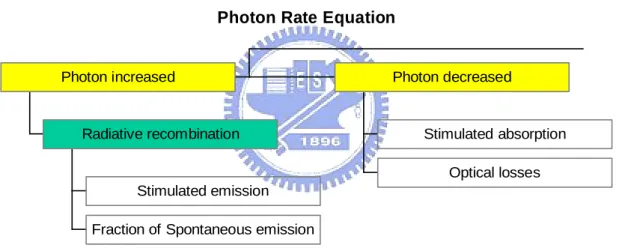
(33) (small bandgap). For comparison, GaAs lasers generally emit between 800 to 860 nm. If we restrict our attention to GaAs then R Auger term can be neglected. We will usually rewrite Eq.(2-10) as: Fraction of Rspon = βBN 2 ≅ β. N. (2-15). τN. 2.1.5 Photon Rate Equation Many of the processes that decrease the carrier density N in the active volume Va must also increase the photon density S in the modal volume Vm . Figure 2.9 shows all the individual terms contribute to the photon rate equation.. Photon Rate Equation. Photon increased. Photon decreased. Radiative recombination. Stimulated absorption Optical losses. Stimulated emission Fraction of Spontaneous emission. Fig. 2.9. The individual terms considered by general photon rate equation.. We can therefore write a photon rate equation as:. dS = radiative recombination − photon decrease dt Stimulatede emission ⎛ ⎞ ⎛ Stimulated absorption ⎞ = ⎜⎜ ⎟⎟ − ⎜ ⎟ ⎝ + Fraction of spontaneous emission ⎠ ⎝ + optical losses ⎠ ⎛ Stimulatede emission ⎞ =⎜ ⎟ + Fraction of spontaneous emission − optical losses ⎝ − Stimulated absorption ⎠ = Γ( Rstim + Fraction of Rspon ) − Opticalloss. 20. (2-16).
(34) where the optical confinement factor Γ specifies the fraction of the optical mode that overlaps the gain region (active region). In other words, the confinement factor gives the percentage of the total optical energy found in the active region Va , it can be expressed as Γ = Va Vm . The term Opticalloss describes the changes of the photon density in each second by optical loss mechanisms, such as light scattering through the sidewall, free carrier absorption, mirror loss, etc, is given by 1 1 × length volume 1 1 unit : × time volume. Opticalloss = (α int + α m ) S. unit :. = (α int + α m )v g S =. (2-17). S. τs. By defining τ s. −1. = (α int + α m )v g , where τ s is photon lifetime, α int is internal loss. due to sidewalls or free carrier absorption, α m is mirror loss ( both top and bottom mirrors), given. αm =. 1 1 ln( ) L R1 R2. (2-18). where L is cavity length, R1 and R2 are the reflectivity of top and bottom mirrors, respectively. By substituting Eq.(2-8),(2-15) and (2-17) into Eq.(2-16) and organize all the terms, obtain photon rate equation as: dS = Γ( Rstim + Fraction of Rspon ) − Opticalloss dt N (t ) − N tr N S = Γ( g 0 )− × S (t ) × v g + β 1 + εS ( t ) τN τs. (2-19). here the RSRH and R Auger are neglected. For convenience, let’s write the carrier rate equations Eq.(2-14) and photon rate equation Eq.(2-19) together, given Eq.(2-20) as:. 21.
(35) Radiative recombination Carrier injection. Stimulated recombination. Spontaneous recombination +Non-radiative recombination. N (t ) − N tr N (t ) ⎧ dN (t ) ηi I (t ) = − − ν S ( t ) g 0 g ⎪ dt τN qVa 1 + εS ( t ) ⎪ ⎨ ⎪ dS (t ) = Γν g S (t ) g0 N (t ) − N tr + Γβ N (t ) − S (t ) ⎪⎩ dt τN τS 1 + εS ( t ) Stimulated emission. Spontaneous emission. (2-20). Optical losses. Eq.(2-20) is same as Eq.(2-1). It represents the general laser rate equation with all the terms and associated phenomena. It can help us to simulate the static-state and dynamic properties of VCSELs. However, the capability of Eq.(2-20) is limited due to it does not take spatial consideration into account. Marc Xavier Jungo have proposed spatiotemporal model of VCSELs in 2003 which is a 2D, multimode, time-domain model, given in Eq.(2-21). Many of VCSELs properties can be investigated in his theoretical research [4]. ⎧ ⎪ ∂N ( r,θ , t ) ηi I ( r ,θ , t ) N ( r,θ , t ) = − ν g ∑ Sm ( r,θ , t )Gm ( N , Sm ) − + DN ∇ 2 N ( r , θ , t ) ⎪ τN ∂t qVa m ⎪ ⎪⎪ ∂S ( r,θ , t ) N ( r ,θ , t ) Sm ( r ,θ , t ) = Γmν g Sm ( r ,θ , t )Gm ( N , Sm ) + Γm β m − ⎨ τN τ Sm dt ⎪ ⎪ N ( r,θ , t ) − N tr (2-21) ⎪Gm ( N , Sm ) = g 0 π R ε ⎪ 1 + 2 ∫ ∫ Sm ( r,θ , t ) rdrdθ ⎪⎩ πR −π 0. where DN is ambipolar diffusion coefficient, the suffix m represents the related parameters for m th mode. In generally, there are several modes contribute to laser’s intensity. Each mode has its own frequency and optical profile. They play a very important role for coupling properties and other practical applications. The multimode behavior of VCSELs is dominated by the interaction of spatially inhomogeneous carrier diffusion and optical field distribution which can’t be represented in Eq.(2-20). The radial and azimuthal distribution (2D) of carriers and photons for individual mode are considered in Eq.(2-21). It accounts for the phenomenon of inhomogeneous distribution of carriers and photons in the active layer and help us to understand how the spatial hole burning (SHB) and multimode operations to affect the static and 22.
(36) dynamic properties of VCSELs. However, Eq.(2-20) is still very important for one to know how to build up the models of VCSELs base on the theory of lasers phenomenology. Due to the understanding of general laser rate equations, one can easily to translate it to Eq.(2-21). Regarding the exact mathematical derivation and formulation of the core model as well as of the advanced mechanisms can be found in [4].. 23.
(37) 2-2 Small signal modulation 2-2-1 Transfer function Under small signal modulation, the carrier and photon density rate equation, are used to calculate relaxation resonance frequency and its relationship to laser modulation bandwidth. Consider the application of an above-threshold DC current, I0, carried with a small AC current, Im, to a diode laser. Illustration is, shown in Figure 2-5, under basic L-I characteristics (Light output power versus current). The small modulation signal with some possible harmonics of the drive frequency, ω. Small signal approximation, assumes Im<<I0 bias and spontaneous emission term, β, is neglected, is expressed as. I = I 0 + I m ( t ) = I 0 + I m ( ω )e jωt n = n0 + nm ( t ) = n0 + nm ( ω )e jωt. (2-22). n p = n p 0 + n pm ( t ) = n p 0 + n pm ( ω )e jωt. Before applying these equations, the rate equation is rewritten for the gain. Assumption under DC current is sufficiently above threshold that the spontaneous emission can be neglected. Without loss of generality, we suppose full overlap between the active region and photon field, Γ =1; furthermore, internal quantum efficiency, ηi , is neglected. That is,. dn I n = − − g0( n − ntr )np dt qV τ dn p. (2-23). = g 0 ( n − n tr )n p + β R sp −. dt substitute Eq. (2-8) into Eq. (2-9). np. (2-24). τp. d( n0 + nm ) ( I 0 + I m ) ⎛ n0 + nm ⎞ = −⎜ ⎟ − g 0 ( n0 + nm − ntr )( n p0 + n pm ) dt qV ⎝ τ ⎠ n ⎛ I = ⎜⎜ 0 − g 0 ( n 0 − n tr ) n p 0 − o τ ⎝ qV. n ⎞ ⎛ Im ⎟⎟ + ⎜⎜ − g 0 ( n 0 − n tr ) n pm − an p 0 n m − m τ ⎠ ⎝ qV. for this, it is similarly expressed modulation terms as dn m I n = m + g ( n 0 )n pm − g 0 n p 0 n m − m dt qV τ. dn pm dt. = g 0 n p 0 n m + g ( n 0 )n pm −. n pm. τp 24. ⎞ ⎟⎟ ⎠. (2-25) (2-26).
(38) The small signal terms in frequency domain of carrier and photon are given by nm ( t ) = nm ( ω )e jωt. n pm ( t ) = n pm ( ω )e jωt substitute into Eq. (2-25) and (2-26), the equations become I m ( ω )e jωt n ( ω )e jωt + g ( n 0 )n pm ( ω )e jωt − g 0 n p 0 n m ( ω )e jωt − m τ qV Carrier modulation term in frequency domain is simplified as jωn m ( ω )e jωt =. jωn m ( ω ) =. Im (ω ) n (ω ) + g ( n 0 )n pm ( ω ) − g 0 n p 0 n m ( ω ) − m qV τ. I (ω ) 1⎞ ⎛ + g ( n 0 )n pm ( ω ) ⎜ jω + g 0 n p 0 + ⎟n m ( ω ) = m qV τ⎠ ⎝ Photon modulation term in frequency domain is simplified as jωn pm ( ω ) = g 0 n p 0 n m ( ω ) + g ( n 0 )n pm ( ω ) − ⎛ ⎜ jω − g ( n 0 ) + 1 ⎜ τp ⎝. (2-27). n pm ( ω ). τp. ⎞ ⎟ n pm ( ω ) = g 0 n p 0 n m ( ω ) ⎟ ⎠. (2-28). Solve for nm(ω) and npm(ω) using Eq. (2-27) and (2-28), we obtain the frequency response of two arranged equations as below. ⎛ jω nm ( ω ) = ⎜ ⎜ jωΩ − ω 2 − ω 2 r ⎝. ⎞⎛ I m ( ω ) ⎞ ⎟⎜ ⎟ ⎟⎜⎝ qV ⎟⎠ ⎠. ⎛ τ pω r 2 ⎜ wheren pm ( ω ) = ⎜ jωΩ − ω 2 − ω 2 r ⎝ ⎛ ⎞ n ω r 2 = ( 2π ⋅ fr )2 = ⎜ p 0 ⎟g 0 ⎜ τp ⎟ ⎝ ⎠ Ω=. 1. ⎞⎛ I ( ω ) ⎞ ⎟⎜ m ⎟ ⎟⎜⎝ qV ⎟⎠ ⎠ ……Relaxation frequency. (2-29) (2-30). (2-31) (2-32). + n p 0g 0. ……Damping constant (decay rate). τ With the Eq. (2-29) and (2-30) we observe the coupling between the small signal photon, npm, and carrier, nm. Small signal carrier injection induces photon achieved oscillation. This phenomenon produces a natural resonance in the laser cavity which shows up the output power of the laser in response to sudden changes in the input current. The natural frequency of oscillation associated with this mutual dependence between nm and npm. Modulation response is expanded the small signal modulation 25.
(39) relationship to steady-state. From Eq. (2-29) and (2-30), the modulation response is denoted as τ pωr 2 2 npm ( ω ) ωr 2 jωΩ − ω 2 − ωr = = M( ω ) = 2 npm ( 0 ) jωΩ − ω 2 − ωr τ pωr 2 ωr 2 (2-33) Modulation bandwidth is determined as cutoff frequency, fc, which is the position with half response written as M ( ωc ) =. ωr 2 1 1 1 M( 0 ) = = 2 2 ⎡ ω 2 − ω 2 2 + ω 2Ω 2 ⎤ 2 r r ⎢⎣ c ⎥⎦. (. ). for ωr2Ω2 << (ωc2-ωr2)2, the cutoff frequency, ωc, is approximated to. (2-34). 3 ωr.. Transfer function, H(ω), is the identical term in Eq. (2-25) and (2-26) respectively obtained with Cramer’s rule. It is similar to modulation response, M(ω), describing the response of the laser intensity to small variations in the drive current through the active region. That is,. fr. H( f ) = C. 2. (2-35) f γ 2π where fr is the resonance frequency same as Eq. (2-31), γ is the damping rate similar to Eq. (2-32), and C is a constant. Accounting for additional extrinsic limitations due to carrier transport and parasitic elements related to the laser structure results in an extra pole in the small signal modulation transfer function. fr − f 2 + j 2. ⎞ ⎛ ⎞ ⎛⎜ ⎟ 2 ⎜ ⎟ f 1 ⎟ ⎜ r ⎟⋅ H ( f ) = C⎜ ⎜ f ⎟ f ⎟ ⎜ 2 2 (2-36) γ ⎟ ⎜⎜ 1 + j ⎟⎟ ⎜ fr − f + j fp ⎠ 2π ⎠ ⎝ ⎝ where fp is the cutoff frequency of the low pass filter characterizing the extrinsic limitations. It is crucial for microwave applications that the modulation bandwidth of the VCSEL is sufficiently large so that efficient modulation is achieved as the modulation frequency.. 26.
(40) 2.3 Relative Intensity Noise (RIN). The measurement of relative intensity noise (RIN) describes the laser’s maximum available amplitude range for signal modulation and serves as a quality indicator of laser devices. RIN can be thought of as a type of inverse carrier-to-noise-ratio measurement. RIN is the ratio of the mean-square optical intensity noise to the square of the average optical power: RIN =. < ∆P 2 > dB / Hz P2. (2-36). where <∆P2> is the mean-square optical intensity fluctuation (in a 1-Hz bandwidth) at a specified frequency, and P is the average optical power. It is more convenient to define RIN per unit bandwidth because the measurement bandwidth can vary under different experimental conditions. As defined, RIN is measured in dB/Hz. Relative intensity noise measurements represent the alternative technique used for studies of high-speed dynamics in semiconductor lasers. Like modulation response technique described above this approach allows for determining of dG/dn and K-factor through numerical fitting procedure. However, the signal measured is not response to the external modulation of the bias current but noise spectra of the laser itself. This noise power is associated with the fluctuation of the concentrations in photon and electron systems caused by spontaneous light emission events. Deviation of the electron and photon densities from equilibrium values leads to their damped oscillations with the frequency of electron-phonon resonance and damping factor. Hence, the measurements of the laser noise power spectra at different bias currents provide enough information to determine such important laser parameters as differential gain and K-factor. Small signal analysis applied to the rate equations, but taking into account internal noise source and transport of carriers leads to the following expression for the spectral dependence of the RIN:. RIN =. 4. π. δf st. f 2 + (γ / 2π ) 2 ( fr. 2. − f 2 ) 2 + f 2 (γ / 2π ). (2-37). where - δfst - Schawlow-Townes linewidth and * g - differs from g in denominator due to carrier transport through the active region of modern MQW laser . The main advantage of the RIN technique with respect to modulation response measurements is the elimination of the problem by high frequency modulation experimental equipment. At the same time, low level of the noise for high quality lasers makes it is necessary to use low noise preamplifiers. Also, there is no low 27.
(41) frequency rolloff in the RIN spectra, which is related to the carrier capture and diffusion across SCH time.. References. 1. 2. 3. 4.. BAHAA E. A. SALEH, MALVIN CARL TEICH, “ Fundamentals of Phtonics,” John Wiley & Sons, Inc., 1991. Siu Fung Yu, “ Analysis and design of vertical cavity surface emitting lasers,” John Wiley & Sons, Inc., 2003. Govind P. Agrawal, Niloy K. Dutta, “Semiconductor lasers,” 2nd edition, AT & T, 1993. Marc Xavier Jungo, “ Spatiotemporal VCSEL Model for Advanced Simulations of Optical Links,” Hartung-Gorre Verlag Konstanz, 2003.. 28.
(42) CHAPTER 3. Experimental facility and setup. 3.1 Inductively coupled plasma reactive ion etching The ICP etching equipment was a planar ICP-RIE system (SAMCO ICP-RIE 101iPH) as shown in Figure 3-1. The ICP main system is consisted of the source chamber and plasma chamber. The source chamber is constructed with RF generation and matching unit including vacuum pumping system, gas transportation system, and cooling water system. (1) Plasma source system The ICP power and bias power source with RF frequency were set at 13.56 MHz. The output RF power introduce into the tornado coil through impedance match and RF power transmission line. The high density plasma was formed by the tornado coil using the theory of inductively coupled plasma. The tornado coil was fixed in the source chamber connecting with ground, and the source chamber has the electromagnet field shielding effect. Between the source chamber and plasma chamber, there is the quartz window to be as the separation. (2) Vacuum pumping system The vacuum pumping system was constructed with mechanical pump and turbo pump. There is a automatic pressure controller (APC) between the plasma chamber and pump. It could control the pumping rate by tuning the throttle inside the APC. The throttle and the pressure meter on the plasma chamber assemble a feedback control system. (3) Gas transportation system Gas transportation system controls the flow rate of the gas source by the mass flow controller (MFC) and the entering of the gas source is decided by a control valve. The MFC and control valve can control the flux and time of the gas source. During the experiment, the pressure of the plasma chamber is set by tuning the APC and the MFC which control the flow rate of the gas source. (4) Cooling water system During the experiment, some equipment must be continuously cooling and sure to be normal operating to prevent the damage, for example the RF generation and turbo pump. And the source chamber and plasma chamber should not be too hot; they also need to remove the heat by the circulating of the cooling water system. 29.
(43) (5) Wafer transportation system In the lab, the load lock chamber is set for keeping the high vacuum of the plasma chamber and enhances the convenience of the operation. The wafer transportation system contains the load lock chamber, the gate valve, the transportation arm. 3.2 Ion implantation system The basic requirement for an ion-implantation system is to deliver a beam of ions of a particular type and energy to the surface of a wafer. Figure 3-2 shows a schematic view of a medium-energy ion implanter. Following the ion path, we begin with the left-hand-side of the system with the high-voltage enclosure containing many of the system components. A gas source feeds a small quantity of source gas such as BF3 into the ion source where a heated filament causes the molecules to break up into charged fragments. This ion plasma contains the desired ion together with many other species from other fragments and contamination. An extraction voltage, around 20 kV, causes the charged ions to move out of the ion source into the analyzer. The pressure in the remainder of the machine is kept below at 10-6 Torr to minimize ion scattering by gas molecules. The magnetic field of the analyzer is chosen such that only ions with the desired charge to mass ratio can travel through without being blocked by the analyzer walls. Surviving ions continue to the acceleration tube, where they are accelerated to the implantation energy as they move from high voltage to ground. Apertures ensure that the beam is well collimated. The beam is then scanned over the surface of the wafer using electrostatic deflection plates. The wafer is offset slightly from the axis of the acceleration tube so that ions neutralized during their travel will not be deflected onto the wafer. A commercial ion implanter is typical 6m long, 3m wide, and 2m high, consumes 45 kW of power, and can process 200 wafers per hour (dose 1015 ions/cm2). Three quantities define an ion implantation step: the ion type, energy, and dose. Given an appropriate source gas, the ion type is determined by magnetic field of the analyzing magnet. In a magnetic field of strength B, ions of charge Q move in a circle of radius R, where RB =. M 1ν 2 M 1V = Q Q. (3-1). where V is the ion velocity and V is the source extraction voltage. The magnetic field is adjusted so that R corresponds to the physical radius of the magnet for the desired 30.
數據
+7

相關文件
An OFDM signal offers an advantage in a channel that has a frequency selective fading response.. As we can see, when we lay an OFDM signal spectrum against the
Wet chemical etchings are especially suitable for blanket etches (i.e., over the whole wafer surface) of polysilicon, oxide, nitride, metals, and Ⅲ-Ⅴ compounds. The
Seals, if any, essential for sealing the pressure sensing element, and in direct contact with the process medium, made of or protected by aluminum, aluminum alloy, aluminum
如圖,已知平行四邊形 EFGH 是平行四邊形 ABCD 的縮放圖形,則:... 阿美的房間長 3.2 公尺,寬
z 香港政府對 RFID 的發展亦大力支持,創新科技署 06 年資助 1400 萬元 予香港貨品編碼協會推出「蹤橫網」,這系統利用 RFID
[r]
You can see that initially the graphs of y = and y = ln x grow at comparable rates, but eventually the root function far surpasses the logarithm. Figure 5
interpretation of this result, see the opening paragraph of this section and Figure 4.3 above.) 2... (For
![TraditionalMLCalgorithmsmainlytacklethebatchMLCproblem,wheretheinputdataarepresentedinabatch[24,28].Nevertheless,inmanyMLCapplicationssuchase-mailcategorization[22],multi-labelexamplesarriveasastream.Onlineanalysisistherefore dimensionreducermotivatedbyma](data:image/gif;base64,R0lGODlhAQABAIAAAP///wAAACH5BAEAAAAALAAAAAABAAEAAAICRAEAOw==)