Using N-Type Organic Material with Photoconductivity for Low
Reflectance OLEDs
Kai-Hsiang Chuang
a, Yu-Hsuan Ho
a, Jiun-Haw Lee
a*, Chun-Chieh Chao
b, Man-Kit Leung
b,
Cheng-Yu Li
c, and Hsuen-Li Chen
ca
Graduate Institute of Electro-Optical Engineering and Department of Electrical Engineering,
b
Department of Chemistry,
cDepartment of Chemistry Department of Materials Science, National
Taiwan University, No. 1, Sec. 4, Roosevelt Road, Taipei, Taiwan, R.O.C.
ABSTRACT
In this paper, we have demonstrated a low-reflectance organic light-emitting device (OLED) by inserting a perylene diimide derivative between the emitting layer (EML) and the cathode. Such a material exhibits a good electron transport capability and good photoconductivity which absorbs light. A semi-transparent layer composed of thin aluminum (Al) and silver (Ag) was used between the EML and the n-type organic material, a perylene diimide derivative, for better electron injection and efficient destructive interference. The J-V characteristics of our low reflection and the control one are nearly identical which shows the superior conductivity of this material. In addition, the absorption peak of this n-type organic material is near 550 nm and is strong enough to absorb nearly half of the ambient visible light. Furthermore, through either interference destruction or directly self-absorption, the photocurrent is generated from the N-type organic material. Thus, this device can also be applied as a photodetector or the applications of the self-adjustable display under different ambient illumination with suitable driving scheme.
Keywords: organic light-emitting device, low reflection, photovoltaic
1. INTRODUCTION
Organic light-emitting device (OLED) has some specific features that make it superior to other competitors in the next generation display or lighting technology [1-2]. A high reflection metals, such as Al, Ag, and Mg:Ag, was typically used as an efficient electron injection cathode in OLEDs [1]. These high reflectance metal cathodes reflect the ambient light and decrease the contrast ratio of OLEDs under the strong ambient environment. And the high reflected ambient light results in low contrast ratio of an OLED which limits the outdoor applications of it. To decrease the ambient reflection, a circular polarizer film attached on the OLED is commonly used [3]. However, it adds extra cost and fabrication complexity in the devices. Thus, we would prefer to adapt the technique which could be integrated into the OLED process to fabricate a low reflection OLED [4-15]. In general, we could separate these high contrast OLEDs into two categories. (1) Light absorbing layer [11-15], (2) Metal-Organic-Metal (MOM) structure [4-10]. The principle of first category is inserting a functional layer which absorbs the ambient light to reduce the reflection of device. The principle of second category is to replace the conventional cathode of OLED with a stack of “thin metal-organic electron transport layer-thick metal” cathode (the so-called MOM structure cathode). In this MOM structure cathode, the reflection light from the first semi-transparent thin metal and the reflection light from the second thick metal interference destructively. Thus, this stack of cathode leads to reduce reflection of an OLED. In this work, we will introduce a MOM type cathode high contrast OLED which incorporates an absorptive N-type perylene diimide derivative. The experiment details are given in section 2. Experimental results and the related discussions are presented in section 3. Finally, a summary is drawn in section 4.
*[email protected]; phone 886 2 2363-5251 ext. 540; fax 886 2 2367-7467
Organic Light Emitting Materials and Devices X, edited by Zakya H. Kafafi, Franky So, Proc. of SPIE Vol. 6333, 63331Q, (2006) · 0277-786X/06/$15 · doi: 10.1117/12.682698
2. EXPERIMENT
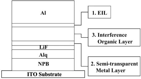
After the pretreatment process by O2 plasma, ITO substrate was transferred into a vacuum thermal evaporator for organic thin-film deposition. During the deposition process around 2x10⁻⁶ torr, we usually control the deposition rate from 0.5 to 2 Å/s for obtaining the sufficient uniform amorphous organic thin film. After finishing the evaporation process, the sample is transferred to the glove box with H2O and O2 concentration lower than 1ppm to encapsulate. The encapsulated devices are measured under atmospheric environment. After device fabrication, B-I-V and lifetime measurements are used to characterize the basic electrical and optical performances of OLEDs. The B-I-V and lifetime system consists of a spectroradiometer (CS-1000), an electrical source-meter (Keithley 2400) and a personal computer. For studying the unusual photocurrent effect of our devices, we measured the I-V characteristics of our devices under the excitation of a 532 nm green laser. For studying the anti-reflectance ability of a device, we use the spectrophotometer (Hitachi U-4100) system to measure the reflectance spectrum of the device. The spectrophotometer, i.e. Hitachi U-4100, can measure the reflectance of device within the wavelength range from ultra-violet to near infrared. Fig. 1 shows the basic configuration of a low reflectance OLED in this study. The low reflection OLED consists of a front control-part and a back MOM structure cathode. The structure of front control-part of our low-reflectance OLED is ITO/ N, N - Bis (naphthalen-1-yl) - N, N – bis (phenyl) benzidine (NPB) (50nm)/ tris (8-hydroxyquinoline) aluminum (Alq3) (40nm)/ LiF (0.5nm). The back MOM structure cathode consists of: semi-transparent thin metal layer/ electron transporting organic layer/ electron injection layer (EIL)/ thick metal layer.
Fig. 1 Device structure of Low-reflection OLED
Table 1 shows the structures of the control OLED (device 1) and low-reflection OLEDs (device 2 to 7) studied in this work. The semi-transparent metal layer has to support a good destructive interference effect and achieve a good electrical connection between the front control part and back cathode part in the devices. Typically, a LiF/Al bi-layer followed by the ETL, Alq3, is needed for better electron injection. Thus, we fabricate a set of low reflection OLEDs by using Al as the semi-transparent metal layer in the MOM structure cathode (device 2 to 6) first. However, the high absorption of Al at visible wavelength makes the MOM structure less preferable to achieve efficient destructive interference effect. For obtaining a good electronic property and further improving the optical characteristics, we fabricated a set of low reflectance OLEDs which adapt an Al/Ag double metal layer (device 7) structure in the semi-transparent layer. Due to the lower absorption and higher transmission of Ag at visible wavelength, replacing the Al layer into the Al/Ag double metal layer in the MOM structure cathode could vary the destructive interference effect efficiently without influencing the electrical properties. In addition, by modulating the ratio of thickness combination in the semitransparent metal layer, we may achieve an optimized anti-reflection OLED further.
ITO Substrate
NPB
Alq
Al
2. Semi-transparent
Metal Layer
3. Interference
Organic Layer
1. EIL
NPB
Alq
LiF
Al
2. Semi-transparent
Metal Layer
3. Interference
Organic Layer
1. EIL
ITO Substrate
NPB
Alq
Al
2. Semi-transparent
Metal Layer
3. Interference
Organic Layer
1. EIL
NPB
Alq
LiF
Al
2. Semi-transparent
Metal Layer
3. Interference
Organic Layer
1. EIL
Table 1. The structures of the devices. (Unit: nm)
Device NPB Alq3 LiF Al Ag N-Type Organic LiF Al
1 0 0 0 0 2 15 3 10 4 5 75 5 10 0 65 6 10 0 7 50 40 0.5 5 5 75 0.5 150
3. RESULTS AND DISCUSSIONS
Fig. 1 shows the J-V curves of the control OLED (device 1) and low-reflection OLEDs (device2 to 4) by using Al as the semi-transparent metal layer in the MOM structure cathode. Operational voltage of device 1 to 4 is 5.9, 6.0, 8.9, and 11.5 V at 50 mA/cm2, respectively. The difference of the operational voltage between control device (device 1) and reflection OLEDs (device 2 to 4) is 0.1, 3, and 5.6V, respectively. Obviously, electrical performances of the low-reflection OLEDs are strongly dependent with the thickness of the semi-transparent metal layer. Thicker the thickness of the semi-transparent metal layer results in better electrical performance. When the semi-transparent layer is increased to 15 nm (device 2), the J-V characteristics is nearly identical to that of the control OLED (device 1) although the total organic layer is thicker in our low-reflection OLED.
-4 -2
0
2
4
6
8
10 12
0
10
20
30
40
50
1 (Control)
2 (Al15/Org.75)
3 (Al10/Org.75)
4 (Al 5/Org.75)
J
(
mA
/c
m
2
)
Voltage (V)
Fig. 1 J-V curves of the control OLED (device 1) and low-reflection OLEDs (device2 to 4) varying the thickness of the
transparent metal layer in the MOM structure cathode.
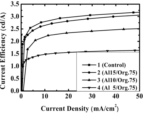
Fig. 2 shows the current efficiency versus current density curves of the control OLED (device 1) and low-reflection OLEDs (device 2 to 4). Current efficiency of device 1 to 4 is 3.16, 3.06, 2.5, and 1.65 cd/A at 50 mA/cm2, respectively. The current efficiency of device 2 to 4 is 96, 79, and 52 %, respectively, of the current efficiency of control device. The reduction of current efficiency of the low reflection OLEDs (device 2 to 4) comes from the photons radiation from the EML towards the cathode will be absorbed or destructed by destructive interference in the MOM structure cathode [16]. Lower current efficiency means the reflection of the MOM is lower, and the OLED is “blacker”. And nearly half current efficiency of the device 4 represents that it has the lowest reflection from the MOM structure with its strongest destructive interference.
0
10
20
30
40
50
0.0
0.5
1.0
1.5
2.0
2.5
3.0
3.5
1 (Control)
2 (Al15/Org.75)
3 (Al10/Org.75)
4 (Al 5/Org.75)
Current Density
(
mA/cm
2)
C
u
rrent
E
ff
ici
ency
(
cd/
A
)
Fig. 2 current efficiency versus current density curves of the control OLED (device 1) and low-reflection OLEDs (device2 to 4) varying the thickness of the semi-transparent metal layer in the MOM structure cathode.
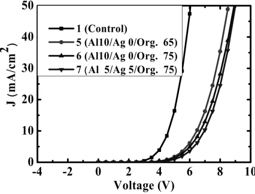
Fig. 3 shows the J-V curves of the control OLED (device 1) and low-reflection OLEDs (device 5 to 7) by using Al/Ag double metal layers, fixing the total thickness at 10 nm, as the semi-transparent metal layer in the MOM structure cathode. Operational voltage of device 1, 5, 6, and 7 is 5.9, 8.5, 8.9, and 9.0 V at 50 mA/cm2, respectively. The difference of the operational voltage between control device (device 1) and low-reflection OLEDs (device 5 to 7) is 2.6V, 3V, and 3.1V, respectively. Form the electrical measurements of this set of devices, we can observe two characteristics: (1) The N-type organic material shows good conductivity due to the nearly identical operational J-V curves of device 5 (N-type organic material = 65 nm) and device 6 (N-type organic material = 75 nm). The operational voltage of the device increases 15 %, as the thickness of N-type organic material in the device increases 15 %. (2) To replace the Al single metal layer into Al/Ag double metal layer will not influence the electrical performance of the low-reflection OLEDs while fixing the total thickness of the semi-transparent metal layer. Thus, we can modify the optical interference
effect of a low-reflection OLED independently through changing the thicknesses of double metals layer in the MOM structure cathode.
-4
-2
0
2
4
6
8
10
0
10
20
30
40
50
1 (Control)
5 (Al10/Ag 0/Org. 65)
6 (Al10/Ag 0/Org. 75)
7
(
Al 5/Ag 5/Org. 75
)
J
(
mA
/c
m
2
)
Voltage (V)
Fig. 3 J-V curves of the control OLED (device 1) and low-reflection OLEDs (device 5 to 7) which adapts an Al/Ag double metal layer, fixing the total thickness at 10 nm, as the semi-transparent metal layer in the MOM structure cathode.
Fig. 4 shows the current efficiency versus current density curves of the control OLED (device 1) and low-reflection OLEDs (device 5 to 7) by using Al/Ag double metal layers, fixing the total thickness at 10 nm, as the semi-transparent metal layer in the MOM structure cathode. Current efficiency of device 1, 5, 6, and 7 is 3.16, 2.64, 2.5, and 1.85 cd/A at 50 mA/cm2, respectively. The current efficiency of device 5 to 7 is 83.5, 79, and 58 %, respectively, of the current efficiency of control device. From these measurements, we can obtain two conclusions: (1) Device 5 and device 6 has different current efficiency due to different thickness of N-type organic material, and device 6 has a lower current efficiency due to its lower reflection, resulting from the stronger absorption of the thicker N-type organic material. (2) The current efficiency of device 7 is 83.5 % of the current efficiency of device 6. That means by using the double metal configuration (device 7) in the MOM structure cathode lowers the reflection value of a low-reflection OLED further. Besides, the J-V curves are nearly identical. Thus, using the double metal configuration as the semi-transparent metal layer provides a good method to reduce the reflection without influences the electrical performance of a low-reflection OLED. Fig. 5 shows the reflectance spectra of the control device (device1) and the low-reflection OLED (device7) which shows the reflectance decreases at all the visible range.
0
10
20
30
40
50
0.0
0.5
1.0
1.5
2.0
2.5
3.0
3.5
1 (Control)
5 (Al10/Ag 0/Org. 65)
6 (Al10/Ag 0/Org. 75)
7
(Al 5/Ag 5/Org. 75
)Current Density
(
mA/cm
2)
C
u
rrent
E
ff
ici
en
cy
(
cd
/A
)
Fig. 4 current efficiency versus current density curves of the control OLED (device 1) and low-reflection OLEDs (device 5 to 7) which adapts an Al/Ag double metal layer, fixing the total thickness at 10 nm, as the semi-transparent metal layer.
300
400
500
600
700
800
0
20
40
60
80
100
R
eflectan
ce(%)
Wavelengh (nm)
1 (Control)
7 (Al 5/Ag 5/Org. 75)
Fig. 5 Reflectance spectra of the control device (device1) and the low-reflection OLED (device7).
3
4
5
6
7
-50
-40
-30
-20
-10
0
10
20
30
40
50
P
ercen
ta
ge o
f I
ncrea
se
m
en
t (
%
)
Voltage (V)
1 (Control)
7
(
Al 5/ Ag 5/ Org. 75
)
Fig. 6 (a) Photocurrent enhancement percentage versus applied voltage of control device (device5) and low reflectance device (device6) (b) Photocurrent enhancement percentage versus applied voltage of low reflectance devices with different thickness of MPPDI layer.
In addition to the good characteristics of our low reflection OLED for display application, our low reflection OLED has the photo effect due to the use of perylene diimide derivative [17]. For further studying the photo effect, we designed an experiment using a 532nm wavelength green laser to pump devices. We define photocurrent enhancement percentage at specific voltage as the difference of the current density between the bright and dark condition over the current density under the dark condition. Fig. 6 shows the photocurrent enhancement percentage of the control device (device 1) and low reflection device (device 7) under the illumination of 532 nm green laser at 60 mW/cm2. The photocurrent enhancement percentage of device 7 at bias 3.6V is 11.5%. On the contrast, device 1 (without N-type organic material) shows no obvious photo-enhancing current at each bias since the control device (NPB/Alq3) do not absorb photons at 532 nm.
4. SUMMARY
We demonstrate a successful low-reflection OLED by using the double metal configuration as the semi-transparent metal layer in the MOM structure. Driving voltage of our low reflection OLED is 3 V higher than the control device while a thick N-type organic material of 75 nm is inserted in such a device. In addition, due to adapt the N-type organic material as the interference and absorption layer, the maximum enhancement of the photocurrent percentage in the optimized low reflection OLED is 11.5% at 3.6V. In contrast, the control device without adapting N-type organic material shows no obviously photocurrent. Thus, the unusual photo-response behavior of this device can be applied as a
photodetector or the applications of the self-adjustable display under different ambient illumination with suitable driving scheme.
ACKNOWLEDGMENTS
This work was financially supported by Chi-Mei Optoelectronics and the National Science Council, R.O.C., under Grant No. NSC 95-2221-E-002-305
REFERENCES
1. C. W. Tang and S. A. VanSlyke, Appl. Phys. Lett., 51, 913 (1987) 2. L. S. Hung and C. H. Chen, Mater. Sci. Eng. R, 39, 143 (2002)
3. C. C. Wu, C. W. Chen, C. L. Lin, and C. J. Yang, J. Dis. Tech., 1, 248 (2005). 4. L. S. Hung and J. Mandathil, Adv. Mater., 13, 1787 (2001).
5. A. N. Krasnov, Appl. Phys. Lett., 80, 3853 (2002).
6. H. Aziz, Y. F. Liew, H. M. Grandin, Z. D. Popovic, Appl. Phys. Lett., 83, 186 (2003).
7. H. M. Grandin, H. Aziz, S. Gardner, C. Jennings, A. J. Paine, P. R. Norton, Z. D. Popovic, Adv. Mater., 15, 2021 (2003).
8. F. L. Wang, M. K. Fung, X. Jiang, C. S. Lee, S. T. Lee, Thin Solid Films, 446, 143 (2004).
9. S. H. Li, H. Liem, C. W. Chen, E. H. Wu, Z. Xu, and Y. Yang, “Stacked metal cathode for high-contrast-ratio polymeric light-emitting devices”, Appl. Phys. Lett., 86, 143514 (2005).
10. K. C. Lau, W. F. Xie, H. Y. Sun, C. S. Lee, and S. T. Lee, “Contrast improvement of organic light-emitting devices with Sm:Ag cathode”, Appl. Phys. Lett., 88, 083507 (2006)
11. X. D. Feng, R. Khangura, Z. H. Lu, “Metal–organic–metal cathode for high-contrast organic light-emitting diodes”, Appl. Phys. Lett., 85, 497 (2004).
12. J. H. Lee, C. C. Liao, P. J. Hu, Y. Chang, “ High contrast ratio organic light-emitting devices based on CuPc as electron transport material”, Synth. Met., 144, 279 (2004)
13. Z. Y. Xie, L. S. Hung, “High-contrast organic light-emitting diodes”. Appl. Phys. Lett., 84, 1207 (2004)
14. Z. Wu, L. Wang, and Y. Qiu, “Contrast-enhancement in organic light-emitting diodes“, Opt. Express, 13, 1406 (2005).
15. C. I. Wu, G. R. Lee, and T. W. Pi, “Energy structures and chemical reactions at the Al/LiF/Alq3 interfaces studied by synchrotron-radiation photoemission spectroscopy”, Appl. Phys. Lett., 87, 212108 (2005)
16. J. H. Lee, C. C. Liao, P. J. Hu, Y. Chang, “ High contrast ratio organic light-emitting devices based on CuPc as electron transport material”, Synth. Met., 144, 279 (2004)
17. C. C. Chao, M. K. Leung, Y. O. Su, K. Y. Chiu, T. H. Lin, S. J. Shieh and S. C. Lin, “Photophysical and Electrochemical Properties of 1,7-Diaryl-Substituted Perylene Diimides”, J. Org. Chem., 70, 4323 (2005)