前瞻性發光元件應用之寬能隙氮化合物材料研究(2/2)
計畫類別: 個別型計畫 計畫編號: NSC92-2215-E-002-010- 執行期間: 92 年 08 月 01 日至 93 年 10 月 31 日 執行單位: 國立臺灣大學光電工程學研究所 計畫主持人: 楊志忠計畫參與人員: Chih-Chung (C. C. ) Yang, Artū;ras Ž;ukauskas and Ivars Tā;le
報告類型: 完整報告
報告附件: 國際合作計畫研究心得報告 處理方式: 本計畫可公開查詢
OF REPUBLIC OF LITHUANIA AND REPUBLIC OF LATVIA WITH
REPUBLIC OF CHINA (TAIWAN)
REPORT
onMATERIALS RESEARCH ON WIDE BAND GAP GROUP III NITRIDE COMPOUNDS FOR ADVANCED LIGHT EMITTERS
SECOND YEAR (2003-2004)
Submitted to: National Science Council, Bonn office, Bonn, Germany National Science Council, Taipei, Taiwan, Republic of China Department of Science and Higher Education under the Ministry of Education and Science, Vilnius, Lithuania
Department of Higher Education & Science of the Ministry of Education and Science, Riga, Latvia
Submitted by: Prof. Dr. Chih-Chung (C. C. ) Yang
Graduate Institute of Electro-Optical Engineering, National Taiwan University, 1, Roosevelt Road, Sec. 4, Taipei, Taiwan, Republic of China
Tel: 886 2 23657624, Fax: 886 2 23652637, E-mail: [email protected] Prof. Habil. Dr. Artūras Žukauskas
Institute of Materials Science and Applied Research, Vilnius University, Sauletekio al. 9, building III, LT-10222 Vilnius, Lithuania
Tel/Fax: 3705 2 366059, E-mail: [email protected] Prof. Dr. Habil. Phys. Ivars Tāle
Institute of Solid State Physics, University of Latvia, 8 Kengaraga Str. LV-1063 Riga, Latvia
Tel: 371 7 260639, Fax: 371 7 112583, E-mail: [email protected]
2
MATERIALS RESEARCH ON WIDE BAND GAP GROUP III NITRIDE COMPOUNDS FOR ADVANCED LIGHT EMITTERS
SECOND YEAR (2003-2004)
CONTENS
Resume
3 I. General part 5 1.1. Introduction 5 1.2. Participants 61.3. Coordination of the project 7
1.4. Brief description of the activities, performed in 2003-2004 year 7
1.5. Publications 8
1.6. Research plan for year 2004-2005 12
II. Detailed description of results and activities 13
2.1 Impact of post grown thermal treatment on luminescence properties of
InGaN multiple quantum wells of various well widths 13 2.2 Photoluminescence line width analysis in InGaN multiple quantum wells
using Monte Carlo simulation of exciton hopping 24 2.3 Quantum-confined Stark effect and localization of carriers selectively
photoexcited into InGaN quantum wells 33
2.4 Thermoactivation spectroscopy of charge localization states in
InGaN/GaN quantum well 33
2.5 Nanostructures and carrier localization behaviors of green-luminescence InGaN/GaN quantum-well structures of various Silicon-doping
conditions 46
2.6 Iprovements of InGaN/GaN quantum well Interfaces and radiative
efficiency with InN interfacial layers 52
3
MATERIALS RESEARCH ON WIDE BAND GAP GROUP III NITRIDE COMPOUNDS FOR ADVANCED LIGHT EMITTERS
SECOND YEAR (2003-2004)
Resume
The joint Lithuanian-Latvian-Taiwanese project on “MATERIALS RESEARCH ON WIDE BAND GAP GROUP III NITRIDE COMPOUNDS FOR ADVANCED LIGHT EMITTERS” addresses materials quality issues of group III nitride semiconductors. A wide-range of optical spectroscopy experiments and theoretical modeling applied enabled us to perform materials characterization in InGaN/GaN quantum well structures used for green-blue light emitting diode and semiconductor laser applications.
During the second year of the project, InGaN/GaN quantum well structures with various well width and indium content, prepared by Taiwan side, were characterized by traditional optical spectroscopy and high-resolution microscopy including strain state analysis. Further, samples were studied by Lithuanian and Latvian groups by applying complementary methods of materials characterization based on photoluminescence, photoluminescence excitation, time-resolved photoluminescence, photoluminescence power excitation, photoreflectance, and modeling by conventional Schroedinger-Poison, Monte Carlo and
ab-initio approches.
Combined materials postgrowth characterization enabled us to give recommendations on InGaN/GaN multiple quantum well thermal treatment. The performed optical and microstructure analysis evidences on an improvement of the MQW structural quality and increased emission efficiency in thicker structures upon post growth thermal annealing. Combined experiments on spontaneous and stimulated emission performed at high intensity excitation together with analysis of the excitation power dependences of luminescence enabled us to estimate increased variation of the random band potential with increasing the well width. Differences in degree of disorder in as-grown samples of various well width were shown to lead to different impact of thermal annealing on luminescence from localized states. The results are accounted for in terms of annealing-invoked In–Ga interdiffusion, which behaves as either diffusion of indium to barriers or “up-hill” diffusion within the wells depending on the well width.
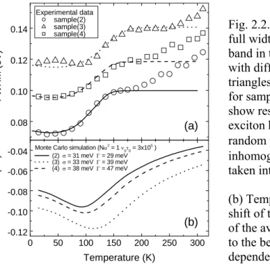
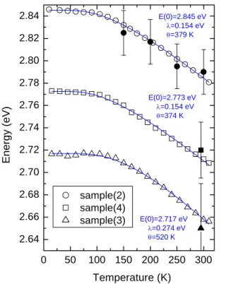
Temperature dependence of the photoluminescence linewidth in thin InGaN/GaN multiple quantum wells was analyzed using Monte Carlo simulation of exciton hopping. The dependence was shown to reveal a crossover from nonthermalized to thermalized exciton energy distribution at about 150 K and fluctuations of the band potential with additional broadening that was attributed to formation of In-rich regions. Based on the fitting procedure, band potential fluctuations within In-rich regions (31 meV) and dispersion of the average exciton energy in different In-rich regions (29 meV) were extracted. The localized-state energy dispersion for hopping of excitons within isolated In-rich regions increase with increasing In content from 31 meV in the sample with the lowest In content to 38 meV in sample with the highest In content. Meanwhile, the dispersion due to different average indium content within the In-rich regions changes from 29 to 47 meV in the same samples, respectively. A Bose-Einstein-like temperature dependence of the exciton energy in the wells was reconstructed and proved by photoreflectance measurements of the mean exciton energy.
The deep level transient spectroscopy (DLTS) for investigation of trapping states in GaN muli quantum well structures has been installed and approved. In order to assess the usability of DLTS technique for study the deep trapping levels in multi-quantum well
4
structures both the thermostimulated depolarization (TSD), thermostimulated capacitance relaxation (TSC) and DLTS are studied in p-n homojunction GaN blue diode. The TSD and TSC curves shows that cooling of the GaInN structure down to liquid helium temperatures results in complete trapping both the majority and the minority charge carriers at the shallow dopand levels. Thermal ionization of the dopand states occurs in the temperature region 40 – 60 K. According to the DLTS data the electron level at Ec-Et=0.3 eV is observed.
Ab initio calculations of the neutral and charged defects in GaN has been provided.The generalized gradient approximation of a density functional theory in LCAO approximation is used to determine electronic structures and formation energies of defects in hexagonal GaN. Formation of localized electronic states followed by localization of excess charge carriers has been considered. Impurities of Mg, Zn, Li, Si and C atoms (the most common dopants) and vacancies of Ga and N are examined. Defects are tested for being centers of an electron localization, therefore calculations of all relevant charged states are done. All calculations are performed for a supercell containing 96 atoms which seems to be enough to neglect defect interaction to its image. Typical atomic relaxations for two nearest neightbours are found to be 4 -5% of the corresponding bond length in a perfect crystal for both impurities and vacancies. Mulliken atomic charge differences are much greater at two nearest neighbours of defect than anywhere else in a crystal. These results imply that such point defects in GaN significantly affect a geometry of only first two coordination spheres.
During the second year, problems of improvement of device performance by Si doping have been addressed. Further study of exciton migration processes together with advanced spectroscopy experiments is foreseen for the next year of the project. Basing on success in understanding of exciton localization and migration processes we believe that performed joint actions on advanced microscopy, optical spectroscopy, and theoretical modeling will enable us to make an significant progress in quantitative characterization of device prototype InGaN/GaN systems.
5
MATERIALS RESEARCH ON WIDE BAND GAP GROUP III NITRIDE
COMPOUNDS FOR ADVANCED LIGHT EMITTERS
SECOND YEAR (2003-2004)
I. General part
1.1 Introduction
New generation of semiconductor materials based on group III-V compounds tremendously expands application areas of direct bandgap semiconductors. In particular, group-III nitrides are subject of a huge interest that is classified as “the blue-UV revolution” in optoelectronics.
The joint Lithuanian-Latvian-Taiwanese project on “MATERIALS RESEARCH ON WIDE BAND GAP GROUP III NITRIDE COMPOUNDS FOR ADVANCED LIGHT EMITTERS” addresses materials quality issues of group-III nitride semiconductors that might improve the competitiveness of each country in the field of production and applications of novel short-wave visible and near-UV light emitters.
The successful fabrication of GaN-based light-emitting devices relies on several novel techniques in the growth and process for the devices. However, application of new generation of ternary (InGaN, AlGaN) and quaternary (InAlGaN) wide-band gap semiconductor materials rise fundamental problems in the control of the materials properties and predictions of device electronic structure. Despite of a significant number of scientific publications that relate to optical properties of group-III nitride based compounds and their nanostructures, fundamental mechanisms responsible for efficient photon emission are not well understood so far. In particular, the role of indium aggregation and phase separation in InGaN system in photon emission efficiency are still quite controversial. Also, the role of the built-in electric field effect on emission properties of light emitting diodes and lasers has been unambiguously not unveiled. On the other hand, further promotion of group-III nitride semiconductors is hindered by insufficient materials quality.
Monitoring of the materials quality as well as of the built-in electric fields in quantum structures is a subject of major efforts undertaken by nitride semiconductor physicists and engineers. A variety of conventional characterization methods, such as high-resolution x-ray diffraction (HRXRD), transmission electron microscopy (TEM), atomic force microscopy (AFM), reflection high-energy electron diffraction (RHEED), photoluminescence (PL), time-resolved luminescence (TRL), photoluminescence excitation (PLE), photoluminescence power excitation (PPE), photo-reflection (PR), are used to a provide a feedback for the fabrication and processing of nitride semiconductor devices.
One of the main goals of the present project is to enhance the arsenal of materials characterization methods such as high-photoexcitation photoluminescence and optical gain, nonlinear optical spectroscopy as well as study of localized and defect states in combination with theoretical modeling of carrier/exciton dynamics. The advancing of combined
6
characterization techniques is expected to promote further improvement of materials quality of AlInGaN semiconductor system.
1.2 Participants: Taiwan group
Prof. C.C. Yang,
Yi-Yin Chung, Shih-Wei Feng, Yung-Chen Cheng, Chih-Wen Liu, En-Chiang Lin
Department of Electrical Engineering and Graduate Institute of Electro-Optical Engineering, National Taiwan University, Taipei, Taiwan, R.O.C.
Yen-Sheng Lin and Cheng Hsu
Department of Mechanical Engineering, Chung Cheng Institute of Technology, National Defense University, Tahsi, Taoyuan, Taiwan, R.O.C.
Kung-Jen Ma
Department of Mechanical Engineering, Chung Hua University, Hsinchu, Taiwan, R.O.C.
Hui-Wen Chuang, Cheng-Ta Kuo, and Jian-Shihn Tsang
Advanced Epitaxy Technology Inc., Hsinchu Industrial Park, Taiwan, R.O.C. Latvian group
Prof. I.Tale,
Dr. phys. M. Springis, Dr. phys. P. Kulis, and Dr. phys. U. Rogulis,
Bn. stud. M. Piesins, Bn. stud. I. Gromulis, M.stud. A. Sarkovskis and M.stud. A. Gulans
Institute of Solid State Physics University of Latvia, Riga, Latvia. Lithuanian group
Prof. A.Žukauskas,
Prof. S.Juršėnas, Prof. G.Tamulaitis, Dr. G.Kurilčik,
Ph.D student S. Miasojedovas, Ph.D student K. Kazlauskas, undergraduate students J. Mickevičius and P. Pobedinskas
7
1.3 Research coordination
Mutual e-mail communications of the group leaders Prof. C. C. Yang, Prof. A. Žukauskas, and Prof. I Tale were employed to coordinate the joint work. Much effort in the second year of the project was paid to integration of experimental abilities and expertise within three groups.
The detailed working plan for the second year was discussed during the visit of Prof . S.Jursenas (Taipei, Taiwan, May 2003). A new set of InGaN/GaN multiple quantum wells varying in In content was selected for detailed spectroscopy experiments and theoretical modeling.
Joint experiments of Latvian and Lithuanian groups were organized by mutual exchange of the samples and visits of Habil Dr. M. Springis to Vilnius (October–November 2003). Summarization and final exchange of the results of the second year on post-growth optical characterization of the multiple quantum wells has been organized by the visits of Prof. S. Juršėnas to Riga in (March 2004) and to Taipei (April to May 2004).
The further work is expected to be discussed by the group leaders during the International Workshop on Nitride Semiconductors IWN2004, July 19-23, 2004 Pittsburgh, Pennsylvania, USA.
1.4 Brief description of the activities performed in 2003-2004 year
The main direction of research performed by Taiwan group in 2003-2004 year was optimization of thermal treatment and doping of the InGaN/GaN multiple quantum well (MQW) structures and microscopy characterization extended with stress strain state analysis images combined with conventional optical characterization methods. Taiwan group supplied the other two groups by high-quality samples of InGaN/GaN MQWs with various well widths and various In content used as device prototypes.
Latvian group concentrated on photoluminescence excitation spectroscopy, and
characterization of charge carrier capture by thermoactivated recombination kinetics in InGaN/GaN heterostructures produced in Taiwan. Ab initio calculations of charged point defects in GaN were fulfilled.
Lithuanian group applied a variety of optical characterization methods for the samples
produced in Taiwan. The main attention was paid to carrier/exciton localization problem, which was addressed by Monte Carlo simulations of temperature dependencies of luminescence spectral features together with the analysis photoreflectivity spectra and results on site-selective luminescence spectroscopy. Carrier dynamics at high-intensity photoexcitation was studied in order to optimize efficiency of stimulated emission under experimental conditions that are typical for semiconductor laser operation regime.
8
1.5 Publications
[1] Shih-Wei Feng, En-Chiang Lin, Tsung-Yi Tang, Yung-Chen Cheng, Hsiang-Chen Wang, C. C. Yang, Kung-Jen Ma, Cheng-Hsing Shen, L. C. Chen, K. H. Kim, J. Y. Lin and H. X. Jiang, “Thermal Annealing Effects of an InGaN Film with an Avearge Indium Mole Fraction of 0.31,” Applied Physics Letters, Vol. 83, No. 19, pp. 3906–3908, 2003.
[2] Yung-Chen Cheng, Shih-Wei Feng, En-Chiang Lin, C. C. Yang, Cheng-Hua Tseng, Chen Hsu and Kung-Jeng Ma, “Quantum Dot Formation in InGaN/GaN Quantum Well Structures with Silicon Doping and Its Implication in the Mechanisms of Radiative Efficiency
Improvement,” Physica Status Solidi C, Vol. 0, No. 4, pp. 1093–1096, 2003.
[3] Shih-Wei Feng, Yung-Chen Cheng, En-Chiang Lin, Hsiang-Chen Wang, C. C. Yang, Kung-Jen Ma, Ching-Hsing Shen, L. C. Chen, K. H. Kim, J. Y. Lin, and H. X. Jiang, “Thermal Annealing Effects on the Optical Properties of High-indium InGaN Epi-layers,” Physica Status Solidi C, Vol. 0, pp. 26540–2657, 2003.
[4] S. Juršėnas, S. Miasojedovas, G. Kurilčik, A. Žukauskas, Shih-Wei Feng, Yung-Chen Cheng, C. C. Yang, Cheng-Ta Kuo, and Jian-Shihn Tsang, “Quantum-well Thickness Dependence of Stimulated Emission in InGaN/GaN Structures”, Physica Status Solidi C Vol. 0, No. 7, pp. 2610–2613, 2003.
[5] Yung-Chen Cheng, En-Chiang Lin, Shih-Wei Feng, Hsiang-Chen Wang, C. C. Yang, Kung-Jen Ma, Chang-Chi Pan, and Kung-Jen-Inn Chyi, “Characteristics of Amplified Spontaneous Emission of High Indium Content InGaN/GaN Quantum Wells with Various Silicon Doping Conditions”, Physica Status Solidi C, Vol. 0, pp. 2670-2673, 2003.
[6] Yung-Chen Cheng, S. Juršėnas, Shih-Wei Feng, and C.C. Yang, Cheng-Ta Kuo and Jian-Shihn Tsang, “Impact of Post-Growth Thermal Annealing on Emission of InGaN/GaN Multiple Quantum Wells”, Phys. Stat. Sol. A, Vol. 201, pp. 221–224 (2004).
[7] Yung-Chen Cheng, En-Chiang Lin, Cheng-Ming Wu, C. C. Yang, Jer-Ren Yang, Andreas Rosenauer, Kung-Jen Ma, Shih-Chen Shi, L. C. Chen, Chang-Chi Pan and Jen-Inn Chyi, “Nanostructures and Carrier Localization Behaviors of Green-luminescence InGaN/GaN Quantum-well Structures of Various Silicon-doping Conditions,” (2004) accepted for publication in Applied Physics Letters.
[8] Shih-Wei Feng, Tsung-Yi Tang, Yen-Cheng Lu, Shi-Jiun Liu, En-Chaing Lin, C. C. Yang, Kung-Jen Ma, Ching-Hsing Shen, L. C. Chen, J. Y. Lin and H. X. Jiang, “Cluster Size and Composition Variations in an InGaN Thin Film of Yellow Emission upon Thermal
Annealing,” (2004) accepted for publication in J. Applied Physics.
[9] K. Kazlauskas, G. Tamulaitis, P. Pobedinskas, A. Zukauskas, Shih-Wei Feng, Yung-Chen Yung-Cheng, C. C. Yang, Yung-Cheng-Ta Kuo and Jian-Shihn Tsang, “Photoluminescence Linewidth Analysis in InGaN Multiple Quantum Wells Using Monte Carlo Simulation of Exciton Hopping,” submitted to Applied Physics Letters
[10] Yung-Chen Cheng, Shih-Wei Feng, C.C. Yang, Cheng-Ta Kuo, Jian-Shihn Tsang, S. Juršėnas, S. Miasojedovas, and A. Žukauskas, “Optical Properties of As-Grown and
9
Annealed InGaN/GaN Multiple Quantum Wells of Various Well Width,” submitted to Semiconductors Science&Technology.
[11] Yung-Chen Cheng, Shih-Wei Feng, C.C. Yang, Cheng-Ta Kuo, Jian-Shihn Tsang, S. Juršėnas, S. Miasojedovas, and A. Žukauskas “Stimulated Emission in InGaN/GaN Multiple Quantum wells With Different Indium Content,” submitted to Acta Physica Polonica A.
[12] Yung-Chen Cheng, Cheng-Ming Wu, Meng-Kuo Chen, C. C. Yang, Zhe-Chuan Feng, Gang Alan Li, Jer-Ren Yang, Andreas Rosenauer, and Kung-Jen Ma, “Improvements of
InGaN/GaN Quantum Well Interfaces and Radiative Efficiency with InN Interfacial Layers,” under revision for publication in Applied Physics Letters.
[13] Hsiang-Chen Wang, Shih-Jiun Lin, Yung-Chen Cheng, C. C. Yang, and Kung-Jen Ma, “Carrier Relaxation in InGaN/GaN Quantum Wells with nm-Scale Cluster Structures”, under revision for publication in Applied Physics Letters.
Conference presentations
[14] S. Juršėnas, G. Kurilčik, S. Miasojedovas, and A.Žukauskas, Shih-Wei Feng, Yung-Chen Yung-Cheng, C. C. Yang, Yung-Cheng-Ta Kuo, and Jian-Shihn Tsang, “Stimulated emission in InGaN/GaN structures with different quantum well width”, E-MRS Fall meeting (Warsaw, Poland, September 15–19, 2003), p.40.
[15] S. Juršėnas,Yung-Chen Cheng, Shih-Wei Feng, and C.C. Yang, Cheng-Ta Kuo and Jian-Shihn Tsang, “Impact of post-growth thermal annealing on emission of InGaN/GaN multiple quantum wells”, E-MRS Fall meeting (Warsaw, Poland, September 15–19, 2003), p.35-36. [16] S. Juršėnas, G. Kurilčik, S. Miasojedovas, and A.Žukauskas, Shih-Wei Feng,
Yung-Chen Yung-Cheng, C. C. Yang, Yung-Cheng-Ta Kuo, and Jian-Shihn Tsang, “Luminescence Spectroscopy of InGaN/GaN Multiple Quantum Wells under High Excitation” 35th
Lithuanian National Conference on Physics (Vilnius, Lithuania, June 12–14, 2003), p. 19. [17] Yung-Chen Cheng, En-Chiang Lin, Shih-Wei Feng, Hsiang-Chen Wang, and C. C. Yang, Kung-Jen Ma, Shih-Chen Shi and L. C. Chen, Chang-Chi Pan and Jen-Inn Chyi, “Effects of Thermal Annealing on InGaN/GaN Quantum Well Structures with Silicon Doping,” The Fifth Pacific Rim Conference on Lasers and Electro-Optics CLEO/PR (Taipei, Taiwan, December 15–19, 2003).
[18] Hsiang-Chen Wang, Cheng-Yeh Tsai, Yung-Chen Cheng, En-Chiang Lin, Shih-Wei Feng, C. C. Yang, Kung-Jen Ma, Cheng-Ta Kuo and Jian-Shihn Tsang, “Femtosecond Pump-Prpbe Studies on Carrier Dynamics in InGaN/GaN Quantum Wells with Indium Aggregated Quantum Dot Structures,“ The Fifth Pacific Rim Conference on Lasers and Electro-Optics CLEO/PR (Taipei, Taiwan, December 15–19, 2003).
[19] Tsung-Yi Tang, Chih-Chung Teng, Shih-Chun Lin, En-Chiang Lin, Meng-Ku Chen, Cheng-Ming Wu, Jiun-Yang Chen, Yung-Chen Cheng, Shih-Wei Feng, C. C. Yang, Kung-Jen Ma, Cheng-Ta Kuo and Jian-Shihn Tsang, “Dependences of Optical and Material Properties on Nominal Indium Content and Well Width IN InGaN/GaN Quantum Well Structures,” The Fifth
10
Pacific Rim Conference on Lasers and Electro-Optics CLEO/PR (Taipei, Taiwan, December 15-19, 2003).
[20] Shih-Wei Feng, En-Chiang Lin, Yung-Chen Cheng, Hsiang-Chen Wang, C. C. Yang, Kung-Jen Ma, Cheng-Hsing Shen, L. C. Chen, K. H. Kim, J. Y. Lin and H. X. Jiang, “Quantum Dot Structures and Optical Properties of a High-Indium InGaN Film,” The Fifth Pacific Rim
Conference on Lasers and Electro-Optics CLEO/PR (Taipei, Taiwan, December 15–19, 2003).
[21] Shih-Wei Feng, En-Chiang Lin, Tsung-Yi Tang, Yung-Chen Cheng, Hsiang-Chen Wang, C. C. Yang, Kung-Jen Ma, Ching-Hsing Shen, L. C. Chen, K. H. Kim, J. Y. Lin and H. X. Jiang, “Optical and Nano-Structures of InGaN Films with Average Indium Contents Higher Than 30 %,” Materials Research Society’s 2003 Fall Meeting (Boston, USA, December 1–5, 2003). [22] Yung-Chen Cheng, En-Chiang Lin, Hsiang-Chen Wang, C. C. Yang, Kung-Jen Ma,
Chang-Chi Pan and Jen-Inn Chyi, “Gain Characteristics of InGaN/GaN Quantum Well Structures with Various Silicon Doping Conditions,” Materials Research Society’s 2003 Fall Meeting (Boston, USA, December 1–5, 2003).
[23] Hsiang-Chen Wang, Cheng-Yeh Tsai, Yung-Chen Cheng, En-Chiang Lin, C. C. Yang, Kung-Jen Ma, Cheng-Ta Kuo and Jian-Shihn Tsang, “Study on Ultra-fast Carrier Dynamics in InGaN/GaN Quantum Wells with Indium Aggregated Quantum Dot Structures,” Materials Research Society’s 2003 Fall Meeting (Boston, USA, December 1–5, 2003).
[24] M. Springis, P.Kulis, I.Tale, “Thermoactivation and Spectroscopy of Charge Localization States in a InGaN/GaN Quantum Well,” NATO Advanced Research Workshop (Vilnius, Lithuania, June 17–21, 2003), p.22.
[25] Yung-Chen Cheng, Horng-Shyang Chen, C. C. Yang, Z. C. Feng, and Gang Alan Li, “Effects of interface thin layers in InGaN/GaN quantum well structures,” The Fifth International Symposium on Blue Laser and Light Emitting Diodes ISBLLED-2004, (Gyeongju, Korea, March 15–19, 2004).
[26] Yung-Chen Cheng, En-Chiang Lin, C. C. Yang, Jer-Ren Yang, Andreas Rosenauer, Kung-Jen Ma, Chang-Chi Pan, and Kung-Jen-Inn Chyi, “Mechanisms of emission enhancement with silicon doping in InGaN/GaN quantum wells,” The Fifth International Symposium on Blue Laser and Light Emitting Diodes ISBLLED-2004 (Gyeongju, Korea, March 15–19, 2004). [27] Yung-Chen Cheng, En-Chiang Lin, C. C. Yang, Jer-Ren Yang, Andreas Rosenauer,
Kung-Jen Ma, Shih-Chen Shi, and L. C. Chen, “Quantum Dot Structures in Silicon-doped
InGaN/GaN Quantum Wells,” 2004 Nano Materials for Defense Applications Symposium & US/Taiwan Workshop (Maui, Hawaii, US, February 19–26, 2004).
[28] Shih-Wei Feng, C. C. Yang, Kung-Jen Ma, Ching-Hsing Shen, L. C. Chen, K. H. Kim, J. Y. Lin, and H. X. Jiang, “InGaN Quantum Dot Structures and Their Optical Properties in InGaN Thin Films,” Photonics West (San Jose, USA, January 2004).
[29] Yung-Chen Cheng, En-Chiang Lin, Meng-Kuo Chen, Cheng-Ming Wu, C. C. Yang, and Kung-Jen Ma, “Optimum design of silicon doping for emission enhancement of InGaN/GaN quantum well light-emitting devices,” Conference on Lasers and Electro-Optics (San
11
[30] Yung-Chen Cheng, En-Chiang Lin, Meng-Kuo Chen, Cheng-Ming Wu, C. C. Yang, and Kung-Jen Ma, “Optimum design of silicon doping for emission enhancement of InGaN/GaN quantum well light-emitting devices,” Conference on Lasers and Electro-Optics (San
Franscisco, May, 2004).
[31] I.Tale, M. Piesins and C.C.Yang. Thermoactivation spectroscopy of charge localization states in InGaN/GaN Quantum Well. International Workshop on Nitride Semiconductors
(Pittsburgh, PA, USA, July 19–23, 2004).
[32] Guļāns, R. A. Evarestov, I. Tāle, C.C Yang. “LCAO calculation of defects in GaN,”
International Workshop on Nitride Semiconductors (Pittsburgh, PA, USA, July 19–23, 2004). [33] A.Sharakovsky,I.Tale, M.Springis, S.Jursenas, C.C.Yang, “Spectroscopy of Charge
Localization States in InGaN/GaN Multiquantum Wells,”ICDIM 2004 (Riga, Latvia, July, 2004).
[34] Guļāns, R. A. Evarestov, I. Tāle, C.C. Yang. Ab initio calculations of charged point defects in GaN. Abstracts of ICDIM 2004 (Riga, Latvia, July, 2004).
[35] A. Zukauskas, K. Kazlauskas, G. Tamulaitis, J. Mickevičius, S. Jursėnas, G. Kurilcik, S. Miasojedovas, M. Springis, I. Tale, Yung-Chen Cheng, Hsiang-Cheng Wang, Chi-Feng Huang, and C. C. Yang, “Carrier Localization Effect in Polarized InGaN/GaN Multiple Quantum Wells”, International Workshop on Nitride Semiconductors (Pittsburgh, PA, USA, July 19–23, 2004).
[36] Hsiang-Chen Wang, Shih-Chun Lin, Yen-Chen Lu, Yung-Chen Cheng, C. C. Yang, and Kung-Jen Ma, “Ultrafast Carrier Relaxation in InGaN/GaN Quantum Wells with nm-scale Cluster Structure,” International Workshop on Nitride Semiconductors (Pittsburgh, PA, USA, July 19–23, 2004).
[37] Yung-Chen Cheng, Meng-Kuo Chen, Cheng-Ming Wu, C. C. Yang, Jer-Ren Yang, Andreas Rosenauer, Kung-Jen Ma, Shih-Chen Shi, L. C. Chen, Chang-Chi Pan and Jen-Inn Chyi, “Differences in Nanostructure and Carrier Localization Behavior of InGaN/GaN Quantum-well Structures with Different Silicon-doping Conditions,” . International Workshop on Nitride Semiconductors (Pittsburgh, PA, USA, July 19–23, 2004).
[38] Yung-Chen Cheng, Cheng-Ming Wu, C. C. Yang, Zhe-Chuan Feng, Gang Alan Li, Andreas Rosenauer, and Kung-Jen Ma, “Improvements of InGaN/GaN Quantum Well Quality and Radiative Efficiency with InN Interfacial Layers,” . International Workshop on Nitride Semiconductors (Pittsburgh, PA, USA, July 19–23, 2004).
[39] K. Kazlauskas, G. Tamulaitis, P. Pobedinskas, A. Zukauskas, Chi-Feng Huang, Yung-Chen Yung-Cheng, Hsiang-Yung-Chen Huang, and C. C. Yang, “Photoluminescence temperature
behavior and Monte Carlo simulation of exciton hopping in InGaN multiple quantum wells,” . International Workshop on Nitride Semiconductors (Pittsburgh, PA, USA, July 19–23, 2004). [40] Yung-Chen Cheng, Shih-Wei Feng, C.C. Yang, Cheng-Ta Kuo, Jian-Shihn Tsang,
S. Juršėnas, S. Miasojedovas, and A. Žukauskas “Stimulated emission in InGaN/GaN multiple quantum wells with different indium content”, Int. Symph. Ultrafast phenomena in semiconductors, UFPS-12 (Vilnius, Lithuania, August, 22–25, 2004).
12
1.6 Research plan for year 2004-2005
Recognition and quantitative theoretical description of localized exciton and defect states in InGaN/GaN device quality structures
Taiwan group
Materials characterization of InGaN/GaN quantum dots;
Stimulated emission measurements for optical gain spectrum and optical gain coefficient calibrations in various In-content and various Si-doping InGaN/GaN multiple quantum well and quantum dot structures;
Study of optical gain coefficient dependence on indium-aggregated cluster density, cluster size and threading dislocation density;
Waveguide implementations. Latvian group
Site selective and photoluminescecnce excitation spectroscopy of InGaN/GaN heterostructures
Electron paramagnetic resonance studies of films in equilibrium and radiation excited states;
Study of the thermostimulated luminescence and thermostimulated depolarization currents versus temperature in III-N samples of different structural quality and composition;
Ab –initio calculations of the electron structure of In quantum dots – like structures in GaN.
Lithuanian group:
Monte Carlo simulation of luminecence transients due to exciton hopping in partially disordered nitride alloys;
Modeling of the impact of Si doping on of exciton hopping In disordered InGaN/GaN heterostructures;
Investigation of the impact of band potential fluctuations on stimulated emission of highly excited in InGaN/GaN MQWs (including Si doped structures) by picosecond time-reslved photoluminescence measurements;
13
II. Detailed description of the results
2.1 OPTICAL PROPERTIES OF AS-GROWN AND ANNEALED
InGaN/GaN MULTIPLE QUANTUM WELLS OF VARIOUS
WELL WIDTH
by
Yung-Chen Cheng, Shih-Wei Feng, C.C. Yang,
Graduate Institute of Electro-Optical Engineering and Department of Electrical Engineering, National Taiwan University 1, Roosevelt Road, Sec. 4,
Taipei, Taiwan, R.O.C
Cheng-Ta Kuo, Jian-Shihn Tsang,
Advanced Epitaxy Technology Inc., Hsinchu Industrial Park, Hsinchu, Taiwan, R.O.C S. Juršėnas, S. Miasojedovas, and A.Žukauskas
Institute of Materials Science and Applied Research, Vilnius University, Saulėtekio al. 9, Building III, LT-10222 Vilnius, Lithuania
Abstract
Site-selective photoluminescence, photoluminescence excitation and time-resolved luminescence in as-grown and thermally treated In0.15Ga0.85N/GaN multiple quantum wells (MQWs) was investigated as a function of well width in the temperature range of 10–300 K. Thermal annealing at 800 ºC for 30 min monitored by microstructure imaging was shown to result in an alteration of MQWs optical properties intricately depending on the well thickness. The observed blue shift of the luminescence band and pronounced changes in the absorbance indicate on remarkable interdiffusion of indium at the quantum well–barrier interface for MQWs with thin (2 nm) wells. Meanwhile for thicker (3 nm) wells, a pronounced red shift of the luminescence band and an increase in the luminescence decay time was observed and attributed to electron–hole wavefunction separation facilitated by the smoothened band potential profile. In the thickest wells (4 nm), annealing resulted in even more pronounced improvement of microstructure, which led to a noticeable reduction of the localization energy of the electronic excitations (an annealing-invoked luminescence peak blue shift that overweighs the red one caused by built-in field) and to suppression of nonradiative recombination (an increase in luminescence efficiency). The results are accounted for in terms of annealing-invoked In–Ga interdiffusion, which behaves as either diffusion of indium to barriers or “up-hill” diffusion within the wells depending on the well width.
2.1.1. Introduction
InGaN-based multiple quantum wells (MQWs) are the key structures for manufacturing of violet, blue, and green light emitting diodes and laser diodes [1,2]. Fabrication of the light-emitting devices requires further optimization of the structures for increased efficiency and lifetime. Thermal treatment is one of the technological factors that may facilitate optimization of active, barrier, and contact layers. Typically during the epitaxial growth of InGaN/GaN structures and during the fabrication of devices, the structures undergo several high-temperature impacts [1]. However, thermal treatment introduced for a particular layer might have an unexpected impact on the other layers. In particular, thermal treatment can change the distribution of the indium composition and influence strain in the quantum wells through ordinary diffusion [3–5] and “up-hill” strain-induced diffusion [6–9].
14
Usually thermal annealing is related to indium and gallium interdiffusion across the interface of quantum-well and barrier layers [3–5]. This results in a blue shift of the photoluminescence (PL) and absorbance spectra [5]. A complete merging of the barrier and well layers has been observed in an InGaN/GaN structure after annealing at high temperature [4]. On the other hand, In–Ga interdiffusion in InGaN alloys is rather intricate because of immiscibility of InN and GaN materials what can result in phase separation in InGaN layers [6,7]. Since InGaN alloys usually are grown at temperatures below 1473 K, the critical temperature above which the InN–GaN system is completely miscible [10,11], in all InGaN alloys phase separation is expected based on thermodynamics considerations. The phenomenon of InGaN phase separation [6–14] is of considerable interest, since InN-rich regions were reported to play a crucial role in light generation in nitride-based light emitting structures [15–19]. Phase separation has been observed using several growth techniques, preferably in thick films [6–9,12]. The observed phase separation is evidently driven by strain due to the mixing of the two lattice mismatched components of the InGaN alloy system. Indium atoms are expelled from the InGaN lattice what results in an occurrence of an alloy of different composition and in reduced strain energy of the system. It has been predicted that for a standard growth temperature, spinodal decomposition occurs for indium concentration above 20% [10,11]. Post-growth thermal annealing was reported to facilitate formation of indium-rich regions in InGaN quantum wells [6–9,13]. On the other hand, thermal annealing can lead to redistribution of strain energy and reduced phase separation, which is sensitive to strain effects. Both phase separation and strain effects are expected to enhance with increasing the InGaN well width. Therefore, the annealing-induced In diffusion mechanism can be well-width dependent.
In the present work, the impact of post growth thermal treatment on optical properties of InGaN/GaN MQWs with various well layer thicknesses was investigated. As grown and annealed samples, which display different images of high-resolution transmittance electron microscopy (HRTEM), were investigated by site-selective PL, observation-energy-selective photoluminescence excitation (PLE), temperature dependent PL, and time-resolved photoluminescence (TRPL). Distinct changes of the MQWs optical properties for the samples of different well layer thickness were linked with the microstructure changes invoked by thermal treatment.
2.1.2. Experimental
The samples were grown on c-plane sapphire by metalorganic chemical vapour deposition. Following the deposition of 30-nm GaN buffer layer and a 2.3-µm GaN layer, MQW structures consisting of five pairs of In0.15Ga0.85N well and 10 nm-thick GaN barrier were grown. Three samples with different well widths of 2, 3, and 4 nm were prepared and referred to as samples w20, w30 and w40, respectively. The growth temperatures were 1010 and 720 0C for GaN and InGaN, respectively. A set of three as-grown samples and three counterpart ones thermally annealed in a quartz tube furnace at 800 ºC in nitrogen ambient for 30 min was investigated.
A cw He–Cd laser (photon energy hν = 3.812 eV) was used for PL excitation. The samples were placed in a cryostat for temperature-dependent measurements. For TRPL measurements, a VerdiTM-laser pumped mode-locked Ti:sapphire laser with 100 fs pulse width and 76 MHz pulse repetition rate with frequency doubling by a BBO crystal was used (hν = 3.177 eV). Luminescence from the sample was collected and focused into a
spectrometer prior to imaging in a Hamamatsu streak camera. The temporal resolution of the operation mode was 4.7 ps. PLE experiments were conducted using quasi-monochromatic excitation light source from a xenon lamp dispersed by a 0.15-m monochromator. The bandwidth of the excitation light from the xenon lamp was set at less than 3 nm.
15
HRTEM investigations were carried out by a 200KeV Philips CM 200 and a 300KeV JEM 3010 microscopes. All the high-resolution micrographs were taken at Scherzer defocus and the sample was viewed along a [11-20] zone axis. The 300keV JEM 3010 microscope was equipped with a 2k×2k slow-scan CCD camera and Gatan Imaging Filter.
2.1.3. Results
A High-Resolution Transmission Electron Microscopy of InGaN/GaN MQWs
According to microstructure analysis performed in the first year study (see Report 2002-2003, Chapter 2.1), HRTM analysis of MQWs was performed for as-grown and annealed samples of various well thicknesses.
The periodic structure of MQWs can be clearly resolved in all images. Typically for ternary InGaN system, the In concentration and strain are rather randomly distributed along MQW layers. Although all our as-grown samples nominally contain the same molar fraction of indium, actual phase separation pattern in the layers of various thickness might be different. Growth of MQWs of a lager thickness requires longer time, thus the quantum well layers have more time for strain relaxation and phase separation. Eventually, more pronounced fluctuations of indium content are expected. This can result in different impact of thermal annealing. The w20 as-grown sample exhibits rather diffusive distribution of strain and indium content, although distinct positions of QWs can be identified. After thermal annealing, the dark areas in the images related to the QWs enhance and occupy a remarkable part of the barrier region. This allows us to make a suggestion about indium interdiffusion in to the barriers and/or enhancement of strained interface regions due to thermal annealing in thin w20 layers.
Thicker MQWs w30 show opposite structural changes under thermal treatment. After thermal treatment, initially large and randomly distributed around QWs dark regions become thinner. This suggests “up-hill” diffusion of indium and/or reduction of strain in the interface regions of thick InGaN/GaN MQWs.
To verify the suggestions that follow from the analysis of microstructure revealed by HRTEM images, below an impact of thermal treatment on optical properties of the MQWs is considered in detail.
B Low temperature site-selective PL and PLE spectroscopy
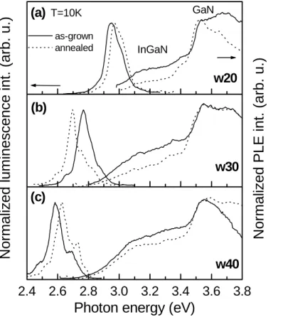
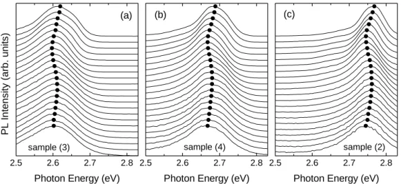
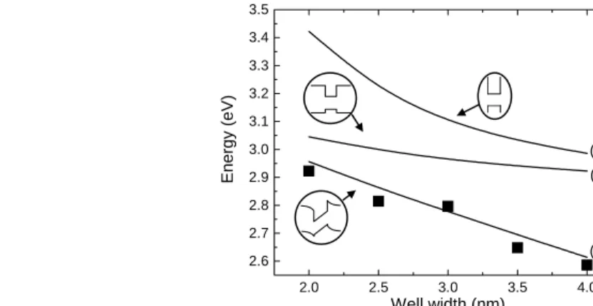
Solid lines on the left-hand side of Fig. 1 show normalized PL spectra of as-grown InGaN/GaN MQW samples obtained at 10 K. The main luminescence spectral properties are typical of low-temperature emission in InGaN/GaN MQWs [16,18,20]. The luminescence spectrum of the w20 sample (Fig. 1(a)) consists of a main band at 2.958 eV, which can be attributed to localized exciton states, and its phonon replica located on the low-energy wing at about 2.865 eV. The band at the high-energy wing of the main luminescence band might be related to shallow impurity related centres [20]. The shape of the spectrum weakly depends on the excitation photon energy (not shown). Meanwhile, the luminescence intensity rapidly decreases with tuning of the excitation photon energy below 3.1 eV as it is seen in the PLE spectra. With increasing the well width of the as-grown samples, the luminescence spectra steadily redshifts with the main peak positioned at 2.767 eV and 2.589 eV for samples w30 (Fig. 1(b)) and w40 (Fig. 1(c)), respectively. The red shift is contributed by several impacts: i) a decrease in quantum confinement energy, ii) the quantum confined Stark effect (QCSE) due to an increase in electron-hole wave function separation caused by built-in field, and iii) deeper localization of the electronic excitations due to an enhancement of disorder-related fluctuations of the band potential profile. At the same time, the bandwidth is seen to decrease with the well width: the estimated full with at half magnitude (FWHM) is 128 meV, 108 meV, and 89 meV for the samples w20, w30, and w40, respectively. The shape of the luminescence
16
band becomes more sensitive to the excitation photon energy with increasing the well width (not shown): the band broadens and blueshifts with an increase of the excitation photon energy. This can be attributed to an enhancement of band potential fluctuations related to growth-time dependent phase separation on the growth surface [8,9].
2.4 2.6 2.8 3.0 3.2 3.4 3.6 3.8
(c)
w40
Photon energy (eV)
T=10K
N
o
rma
liz
e
d
P
L
E
i
n
t. (arb
. u
.)
as-grown annealed (a) w20 InGaN GaN (b) w30Nor
m
aliz
ed lum
inescence int
. (
a
rb
. u.
)
Figure 1. Normalizedphotoluminescence spectra and photoluminescence excitation spectra of as-grown (solid line) and annealed (dotted line) InGaN/GaN MQWs: w20 (a), w30 (b) and w40 (c), measured at 10 K.
Solid lines on the right-hand side of Fig. 1 show PLE spectra of the w20, w30, and w40 as-grown samples. The PLE spectra exhibit typical dependences of MQW structures with spectral variation in optical density of the QW (InGaN) and barrier (GaN) materials reflected. The PLE signal is much stronger for the excitation photon energy above 3.5 eV due to the larger thickness of the barrier layer (10 nm). The boundary between the PLE features of InGaN and GaN layers is sharp due to the edge of excitonic absorbance in GaN. The absorbance edge of InGaN material below 3.1 eV is less steep indicating on the presence of compositional fluctuations, which were seen in the HRTEM images.
With an increase in well width from 2 nm to 4 nm, pronounced changes can be revealed in the well absorbance region: i) an increase in PLE signal due to increased optical density of the InGaN layer; ii) a redshift of about 66 meV that is in line with the quantum confinement effect (note, that built-in electric field can also affect excitonic absorbance spectrum); iii) a pronounced sensitivity of the PLE signal intensity to the observation photon energy (not shown). The latter effect is due to aforementioned sensitivity of the shape of the luminescence band to the excitation photon energy in thicker wells, what is an indication of increased disorder.
In addition, a pronounced difference in the PLE signal caused by absorbance in the GaN barrier layers (hν > 3.50 eV) is peculiar for different well widths. Instead of a rising
dependence, which is predictable for a MQW structure of good quality, a significant decline of the PLE signal for the excitation photon energy above 3.50 eV is observed in the as-grown structures with increased well width. This can be attributed to an enhancement of nonradiative capture of just photogenerated excitons (electrons and holes) with a higher initial excess
17
energy. To produce luminescence from the QW states, the excitons (carriers) excited in the barrier layer are to be captured in the well. However, excitations with a larger excess energy have a smaller well-capture probability and, consequently, a higher overall probability of trapping to nonradiative centres. Thus, the decline in the PLE spectra for hν > 3.50 eV can be
explained under assumption that increased well width results not only in reduced quality of the well material but of the barrier and/or interface also. This is in line with the HRTEM images (Fig. 2(a)–(c)) where an increased patterning of the barrier layers in the as-grown samples with increased well width can be distinguished.
Dotted lines in Fig. 1 show normalized PL and PLE spectra of annealed InGaN/GaN MQWs measured at 10 K. The PL spectrum of the annealed w20 sample blueshifts by about 20 meV in comparison with the as-grown one (Fig. 1(a)). The PL spectrum of the annealed w30 sample redshifts by about 71 meV, while that of the w40 sample blueshifts by about 45 meV. This indicates on an intricate impact of thermal treatment on the luminescence properties of MQWs of various well widths.
The PLE spectra (dotted lines on the right-hand side of Fig. 1) show significant spectral changes as well. (The spectra are normalized at 3.50 eV to reveal spectral changes occurring upon annealing.) The most pronounced impact of thermal treatment appears for the thin-well sample w20 (Fig. 1(a)). A decline of the spectral dependence of the PLE signal in the barrier spectral region at hν > 3.50 eV evidences on a remarkable increase in nonradiative trap
density. This is in line with significant reduction of the luminescence efficiency (see below). Additionally by detailed comparison of the spectra, a blue shift of the PLE feature due to wells at the absorbance edge can be distinguished concurrently with the blue shift of the PL line. These observations support a suggestion drown from the microstructure analysis that thermal treatment results in In interdiffusion from the well layers to the barriers [3–5].
The impact of thermal treatment on the PLE spectra of the thicker QW layers is of opposite character (Fig. 1(b), (c)). The sample w30 shows little changes in the PLE spectrum in the barrier spectral region hν > 3.50 eV, while the even thicker w40 sample shows an
opposite trend: thermal treatment results in a flatter spectral dependence indicating on reduction of the nonradiative traps. Again, this is in line with the narrowing of the dark regions in the HRTM images (Fig 1(c), (f)). The QW absorbance edge becomes flatter for the w30 sample and steeper for the w40 sample. As discussed below, such a behaviour might be due to several impacts such as, indium diffusion, increase in disorder due to composition fluctuations, and electron–hole wavefunction separation due to built-in field.
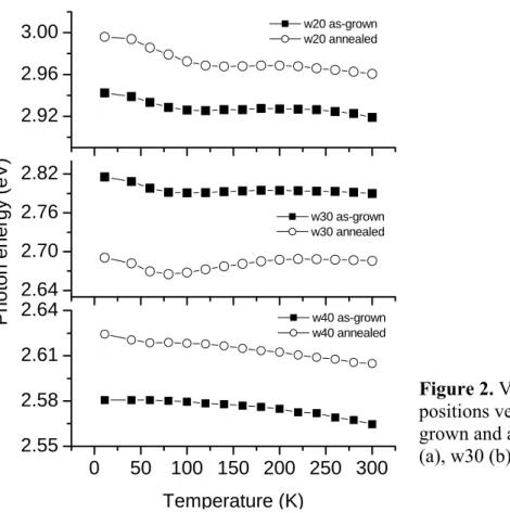
C Temperature dependent PL and TRPL
The temperature variations of the PL peak position in the three pairs of the as-grown and annealed samples are shown in Fig. 2. Both before and after thermal annealing, the characteristic “S-shape” variation of the PL peak can be distinguished in each case indicating on migration of excitations within spectrally and spatially disordered system [21,22]. In both the as-grown and annealed samples, the amplitude of the initial decrease in peak energy diminishes with the well thickness. As revealed by Monte Carlo simulation of exciton hopping [21,22], this can be attributed to an increase in spatial separation between the localized states in thicker wells what is in line with enhanced In segregation seen in HRTEM images. Similar behaviour might be caused by reduced lifetime of the excitons or carriers; however, our TRPL results indicate that lifetime increases with the well width. The “S-shape” becomes more pronounced in the annealed samples. Again, this can be attributed to a decreased spatial separation between the localized states and/or increased lifetime. To our opinion in the thin wells (w20), the major effect is due to increased lifetime (see Fig.4(a)), whereas in the thicker wells (w30 and w40) both effects might be important.
18 0 50 100 150 200 250 300 2.55 2.58 2.61 2.64 Temperature (K) w40 as-grown w40 annealed 2.64 2.70 2.76 2.82 Phot on energy (eV) w30 as-grown w30 annealed 2.92 2.96 3.00 w20 as-grown w20 annealed
Figure 2. Variations of PL peak
positions versus temperature of as-grown and annealed samples: w20 (a), w30 (b) and w40 (c).
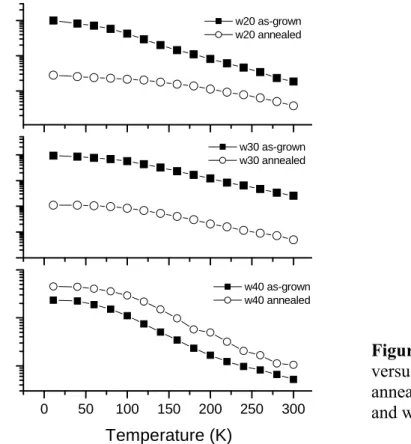
Figure 3 shows temperature-dependent variations of the integrated PL intensity in the as-grown and annealed samples. Thermal treatment is seen to cause a significant reduction in PL intensity in the w20 sample (Fig. 3(a)), in agreement with the suggestion on In interdiffusion and consequent degradation of the barriers and interfaces. Correspondingly, the flatter temperature dependence in the annealed sample is an indication of a larger energy required for delocalization, which facilitates nonradiative recombination [23]. Sample w30 shows similar temperature dynamics (Fig. 3(b)), however without a remarkable change in the activation energy. This can be attributed to an increased role of electron–hole wavefunction separation due to built-in field in thicker wells what agrees with the observed red shift of the PL peak position (Fig. 1(b)). We suggest that such a separation is facilitated by a smoother potential profile in the annealed wells as evidenced by the HRTEM images and temperature dependence of the PL peak position. With further increase in well thickness (sample w40), the principal impact of annealing is an increase of the PL intensity in the entire range of temperatures. In combination with the blue shift of the PL peak position (Fig. 1(c)), such an increase can be attributed to a significant smoothing of the band potential profile and a subsequent decrease of the localization energy. An additional increase in PL intensity might be caused by a reduced number of nonradiative centres in the barrier layers and interfaces what is in agreement with the HRTEM images and PLE spectra.
19 0 50 100 150 200 250 300 Temperature (K) w40 as-grown w40 annealed Lum ine s cence i n tensity ( a rb . u.) w30 as-grown w30 annealed w20 as-grown w20 annealed
Figure 3. Variations of PL intensities
versus temperature of as-grown and annealed samples: w20 (a), w30 (b) and w40 (c).
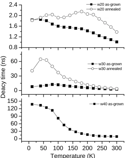
Figure 4 shows PL decay time at the PL spectral peaks as a function of temperature in the as-grown and annealed samples [14]. (In the annealed w40 sample, the PL decay time becomes too long to be measured by our technique.) The low-temperature lifetime of the as-grown samples rapidly increases with the well width and is equal to 1.8 ns, 9 ns, and 137 ns for w20, w30, and w40 samples, respectively. This increase is obviously due to spatial separation of electron and hole wavefunctions in thicker wells (QCSE) [24,25]. This is in line with the increase in Stokes shift with the well width (Fig. 1). Thermal annealing generally results in an increase of carrier lifetime, however, with the peculiarities dependent on the well width. In the w20 sample, the lifetime alters negligibly at low temperature and exhibits a remarkable increase at elevated temperatures. This effect agrees with the temperature dynamics of the PL intensity in that annealing of a thin well results in an enhancement of potential fluctuations and in a higher energy required for delocalization, which initiates the nonradiative process [23]. Interestingly, despite the unchanged lifetime at low temperature, the annealed sample exhibits a lower PL efficiency (Fig. 3(a)), probably because of reduced rate of carrier capture to the well due to degraded barriers and/or interfaces. Contrarily, the thicker wells (w30) show a remarkable increase in low-temperature lifetime after thermal annealing, the difference between the as-grown and annealed samples disappearing with temperature (Fig. 3(b)). Such behaviour might be accounted for by an increased electron–hole wavefunction separation at low temperatures due to increased carrier/exciton diffusivity in the annealed sample. At elevated temperatures, annealing results in negligible changes of lifetime, since the excitations are delocalised. In the thickest sample (w40), localization energy is higher and annealing facilitates the QCSE in the entire temperature range.
20 0 50 100 150 200 250 300 0 30 60 90 120 150 Temperature (K) w40 as-grown 0 30 60 Deacy t im e (ns) w30 as-grown w30 annealed 0.8 1.2 1.6 2.0 2.4 w20 as-grown w20 annealed
Figure 4. Variations of PL decay
times versus temperature of as-grown and annealed samples: w20 (a), w30 (b). That of the as-grown w40 is also shown.
2.1.4. Discussion
Our results on HRTEM, PL, PLE, and TRPL in InGaN/GaN MQWs revealed dynamics of radiative and nonradiative processes with the well thickness and the impact of thermal treatment, which was shown to essentially depend on the quantum well width.
Quantum well width dynamics of recombination processes in InGaN/GaN MQWs is usually explained by the QSCE and inhomogeneous distribution of indium as well as by nonradiative centres due to structural and point defects [15–17, 24–26]. Basically, dynamics of the QSCE with the well width is enough understood for a smooth band potential profile [24,25]. Meanwhile, inhomogeneous distribution of indium, which results in fluctuations of the band potential profile, displays a much more intricate dependence on the well width. There are several studies on accumulation of indium atoms on the growth surface and generation of misfit dislocations with increasing the thickness of the InGaN layer [27,28]. The concurrent plastic relaxation cannot be complete and homogeneous in all regions of the InGaN well, resulting in an inhomogeneous strain distribution within the layer. The inhomogeneous strain distribution could, in turn, enhance the local diffusion of indium atoms and thereby spinodally increases the composition fluctuations. Under favourable conditions, these fluctuations may result in phase separation [8,9]. Phase separation requires long-range diffusion and a correlation should exist between phase separation and the growth time. The larger the layer thickness, the longer growth time is required, thus the quantum well layer has a longer time for strain relaxation and a more pronounced variation in indium content is expected. Our data on optical properties of InGaN/GaN MQWs infer that increasing the well width results in i) increased potential profile fluctuations, which are known to remarkably influence the migration of electronic excitations, ii) a modified nomenclature of nonradiative centres due to
21
indium decomposition and modification of interfaces, iii) enhanced spatial separation of the electron and hole wavefunctions in the wells.
Increased fluctuations of the band potential profile are evidenced by enhanced patterning of the HRTM images, by sensitivity of the PL spectra to the excitation photon energy, sensitivity of the PLE spectra to the observation photon energy, flattening of the well absorbance edge monitored by PLE, and smoothening of the “S-shape” temperature dependence of PL with the increase in the well thickness. The decrease in carrier capture efficiency to the wells due to nonradiative recombination is clearly monitored by changes in the PLE spectrum in the barrier region. Enhanced spatial separation of the electron and hole wavefunctions is evidenced by a significant increase in carrier/exciton lifetime and by a increase in Stokes shift of PL, with both increases partially attributed to increased potential fluctuations. All these observations clearly indicate on an increase in disorder with an increase of the well width.
Differences in degree of disorder of as-grown samples with various well widths leads to different impact of thermal annealing on luminescence from localized states. Since the average indium concentration in our samples is of 15%, only slightly below the critical value [10,11], one can expect different trends in diffusion related processes (diffusion or spinodal decomposition) invoked by thermal treatment. Our data infers that thermal annealing, which basically results in thermally activated In–Ga interdiffusion including “up-hill” strain-induced diffusion and spinodal decomposition, affects microstructure and strain in the wells, barriers and interfaces. Eventually, thermal annealing modifies i) the efficiency of carrier capture to the wells, ii) electron–hole wavefunction separation within the wells, and iii) nonradiative recombination rate, i.e. the basic processes, which govern the quantum efficiency of light generation in InGaN/GaN MQWs.
After thermal annealing, thinner samples that initially are of the best structural and optical quality are heavily deteriorated. We attribute this effect to indium interdiffusion into the barrier layers, what is monitored by the HRTM images. Annealing leads to changes in indium content as evidenced by the blueshift of the InGaN related emission and absorption bands. Indium interdiffusion also results in formation of a large amount of nonradiative defects both in the well and barrier, what is confirmed by a significant reduction in luminescence efficiency and by modification of the PLE spectra in the barrier region. Meanwhile, no indications of changes in spatial separation of electrons and holes were distinguished, probably because of the well thickness too small for the QSCE to manifest itself. Thicker as-grown samples are already much more disordered due to indium segregation. This leads to an increase in the number of surface related defects. Increased thickness results in a noticeable enhancement of the QSCE, what is monitored by the increased carrier lifetime, decreased PL efficiency, and red shift of the PL peak. Annealing seems to improve materials quality and to make potential profile smoother. The smoother potential profile facilitates electron–hole spatial separation, which results in the enhanced QSCE (an increase in the carrier/exciton lifetime, a decrease in PL efficiency, and the red shift of the PL band).
For the thickest samples investigated, thermal annealing results in even more significant improvement of microstructure, what is evidenced by the narrowing of well-related dark regions in the HRTM images, as well as by modification of the barrier related PLE spectrum. This implies that indium is preferentially reorganized in the InGaN layers rather than diffused into GaN barriers. Consequent smoothening of the well potential profile leads to an increased electron–hole spatial separation due to built-in field. However the blue shift of the PL peak and an increase in PL efficiency show that annealing invokes a competing impact that outbalances the manifestation of the QCSE. We attribute this impact to improved
22
microstructure, which results in shallower localization and remedy of nonradiative-recombination centres.
2.1.5. Conclusions
Summarizing, temperature dependent site-selective PL, PLE, and TRPL study of three pairs of as-grown and annealed at 800º C for 30 min In0.15Ga0.85N/GaN MQWs with the well widths of 2, 3, and 4 nm were performed. Our results imply a nontrivial dependence of MQWs emission properties on thermal treatment. Differences in degree of disorder in as-grown samples of various well width leads to different impact of thermal annealing on luminescence from localized states. The blue shift of the PL peak and pronounced changes in the absorbance indicate a remarkable interdiffusion of indium at the quantum well barrier interface for thin MQWs. While the pronounced red shift in PL and an increase in the excitation lifetime in thicker MQWs is attributed to manifestation of the QCSE due to built-in field. Also, MWQs of larger thickness were shown to possess larger variations in potential profile and a larger amount of structural defects. The performed optical and microstructure analysis evidences on
an improvement of the MQW structural quality and increased emission efficiency in the thicker structures upon post growth thermal annealing.
References
[1] Nakamura S and Fasol G 1997 The Blue Laser Diode: GaN Based Light Emitters and
Lasers (Berlin, Springer).
[2] Žukauskas A, Shur M S, and Gaska R 2002 Introduction to Solid-State Lighting (New York, Wiley).
[3] Tsang J-S, Guo J-D, Chan S-H, Feng M-S and Chang C-Y, 1997 Jpn. J. Appl. Phys. 36 1728.
[4] Romano L T, McCluskey M D., Van de Walle C G, Northrup J E, Bour D P, Kneissl M, Suski T and Jun J 1999 Appl. Phys. Lett. 75 3950.
[5] Chou C-C, Lee C-M and Chyj J-I 2001 Appl. Phys. Lett. 78 314.
[6] Singh R, Doppalapudi D, Moustakas T D and Romano L T 1997 Appl. Phys. Lett. 70, 1089.
[7] McCluskey M D, Romano L T, Krusor B S, Bour D P, Johnson N M and Brennan S 1998 Appl. Phys. Lett. 72, 1730.
[8] Doppalapudi D, Basu S N, Ludvig K F Jr. and Moustakas T D, 1998 J. Appl. Phys. 84 1389.
[9] Moon Y-T, Kim D-J, Song K-M, Coi C-J, Han S-H, Seong T-Y and Park S-J 2001 J.
Appl. Plys. 89 6514.
[10] Ho I H and Stringfellow G B 1996 Appl. Phys. Lett. 69 2701. [11] Karpov S Yu 1998 J. Nitride Semicond. Res. 3 16.
[12] Osamura K, Nakajima K and Murakami Y 1972 Solid State Commun. 11 617. [13] Lin Y-S, Ma K-J, Hsu C, Chung Y-Y, Liu C-W, Feng S-W, Cheng Y-C, Mao
M-H, Yang C C, Chuang H-W, Kuo C-T, Tsang J-S and Weirich T E 2002 Appl. Phys.
Lett. 80 2571.
[14] Feng S-W, Chung Y-Y, Liu C-W, Cheng Y-C, Yang C C, Mao M-H, Lin Y-S, Ma K-J, Chyi J-I 2002 Appl. Phys. Lett. 80 4375.
[15] Chichibu S, Azuhata T, Sota T and Nakamura S 1997 Appl. Phys. Lett. 70 2822. [16] Chichibu S, Sota T, Wada K and Nakamura S 1998 J. Vac. Sci. Technol. B 16
2204.
23
[18] Cho Y-H, Schmidt T J, Bidnyk S, Gainer G H, Song J J, Keller S, Mishra U K and DenBaars S P 2000 Phys. Rev. B 61 7571.
[19] Kent P R and Zunger A 2001 Appl. Phys. Lett. 79 1997.
[20] Narukawa Y, Kawakami Y, Fujita S, and Nakamura S, 1999 Phys. Rev. B 59 10283.
[21] Baranovskii S D, Eichmann R and Thomas P 1998 Phys. Rev. B 58 13081. [22] Kazlauskas K, Tamulaitis G, Zukauskas A, Khan M A, Yang J W, Zhang J,
Simin G, Shur M S and Gaska R 2003 Appl. Phys. Lett. 83 3722.
[23] Minsky M S, Watanabe S and Yamada N, 2002 J. Appl. Phys. 91 5176. [24] Bernardini F and Fiorentini V 1998 Phys. Rev. B 58 15292.
[25] Lefebvre P, Morel A, Gallart M, Taliercio T, Allègre J, Gil B, Mathieu H, Damilano B, Grandjean N and Massies J 2001 Appl. Phys. Lett. 78 1252.
[26] Chow W W, Amano H, Takeuchi T and Han J 1999 Appl. Phys. Lett. 75 244. [27] Böttcher T, Einfeldt S, Kirchner V, Figge S, Heinke H, Hommel D, Selke H
and Ryder P L 1998 Appl. Phys. Lett. 73, 3232.
[28] Shimizu M, Kwaguchi Y, Hiramatsu K and Sawaki N 1997 Solid-state electron.
24
2.2.
PHOTOLUMINESCENCE LINE WIDTH ANALYSIS IN InGaN
MULTIPLE QUANTUM WELLS USING MONTE CARLO
SIMULATION OF EXCITON HOPPING
By
A. Zukauskas, K. Kazlauskas, G. Tamulaitis, P. Pobedinskas, S. Jursėnas
Institute of Materials Science and Applied Research, Vilnius University, Vilnius, Lithuania M. Springis, I. Tale
Institute of Solid State Physics University of Latvia, Riga, Latvia
Yung-Chen Cheng, Hsiang-Cheng Wang, Chi-Feng Huang, and C. C. Yang
Graduate Institute of Electro-Optical Engineering and Department of Electrical Engineering, National Taiwan University 1, Roosevelt Road, Sec. 4,
Taipei, Taiwan, R.O.C Abstract
Temperature dependence of the photoluminescence (PL) line width in thin In0.2Ga0.8N/GaN multiple quantum wells (MQWs) was analyzed using Monte Carlo simulation of exciton hopping. The dependence was shown to reveal a crossover from nonthermalized to thermalized exciton energy distribution at 150 K and fluctuations of the band potential with additional broadening that we attributed to formation of In-rich regions. Based on the fitting procedure, band potential fluctuations within In-rich regions (31 meV), dispersion of the average exciton energy in different In-rich regions (29 meV) and a Bose-Einstein-like temperature dependence of the exciton energy in the wells were extracted.
2.2.1. Introduction
InGaN/GaN MQWs are the key components of many commercial devices emitting green, blue, near UV, and white light. It is generally accepted that inhomogeneous distribution of indium facilitates high quantum efficiency of InGaN-based light emitting devices [1]. Formation of In-rich regions in InGaN is proved by high-resolution microscopy and X-ray microanalysis [2,3], spatially resolved cathodoluminescence [4], and near field optical microscopy [5,6]. However despite a tremendous commercial success, InGaN remains a puzzling material mainly because of incompletely unveiled link of its intricate structure with electronic properties. This hinders further improvement of the device performance, which is the key issue for deeper penetration of semiconductor optoelectronics into the lumen market.
PL provides with a deep but experimentally unsophisticated insight into carrier and exciton dynamics in semiconductors. In particular, in group-III nitride alloys and relevant quantum wells, photoluminescence is known to exhibit an anomalous temperature behavior of the peak position (S-shaped dependence) and line width (W-shaped dependence) [7-13] indicating an intricate character of carrier/exciton motion through localized states (hopping) [14-16]. Recently this anomalous behavior received more attention in terms of theoretical modeling of the hopping process. In particular, a double-scaled character of the potential profile was unveiled and parameters of band potential fluctuations were estimated in bulk quaternary AlInGaN alloy by using the Monte Carlo simulation of exciton hopping [17].
We apply the Monte Carlo simulation of exciton hopping for analysis of the PL line width temperature dependence in InGaN MQWs.
2.2.2. Experimental
Narrow quantum wells were chosen for investigation to minimize distortions of the PL spectra due to quantum-confined Stark effect caused by the built-in piezoelectric and spontaneous-polarization fields. The sample was grown by metal-organic chemical vapor
25
deposition over a sapphire substrate and consisted of five 2-nm thick In0.22Ga0.78N quantum wells separated by 9-nm thick GaN barriers deposited on a 2.5 µm thick GaN buffer layer.
A continuous-wave He-Cd laser emitting at 325 nm was used for excitation. The luminescence signal was dispersed by a double monochromator (Jobin Yvon HRD-1) and recorded by using a photomultiplier (Hamamatsu R1463P) in the photon counting regime. A closed-cycle helium refrigerator was employed to perform the measurements at temperatures down to 10 K. To avoid distortions of the PL line shape due to Fabri-Perrot interference caused by multiple reflections of light between the substrate and sample surface (that are ~2.5 µm apart), we collected the PL signal propagating through the transparent substrate that was frosted to randomize the angles of the escaping photons.
The PL excitation spectra were measured by using monochromatized light of tungsten lamp as an excitation source. The measurements were carried out at fixed temperatures down to 8 K by using a closed-cycle helium cryosystem.
The mean exciton position in the samples was determined by using photoreflectance technique. A DSP lock-in amplifier Signal Recovery 7265 was employed in photoreflectance measurements. Reflection of collimated light of a tungsten-halogen lamp was measured under influence of radiation of He–Cd laser (325 nm) modulated by mechanical chopper, which was driven by the lock-in amplifier. The photoreflectance spectra were analysed by using standard procedures [18].
2.2.3. Double-scaled potential in InGaN multipple quantum wells
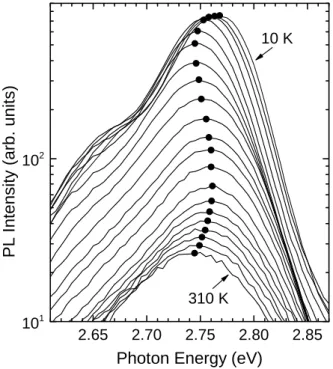
The near-band-edge PL spectra measured at different temperatures are presented in Fig. 2.2.1. The spectra contain a single band with two humps on the low-energy slope separated by approximately 90 meV. We attribute these features to direct and longitudinal-optical-phonon replicated recombination of localized excitons, respectively. The PL intensity maintains an almost stable value below 50 K and decreases at elevated temperatures, most probably, due to enhanced influence of nonradiative recombination.
2.65 2.70 2.75 2.80 2.85 101 102 310 K PL I n tensity (ar b . unit s )
Photon Energy (eV)
10 K
Fig. 2.2.1. Evolution of the PL spectra with temperature in InGaN/GaN MQWs. The
temperature is incremented by 15 K starting with 10 K (the uppermost spectrum) and ending with 310 K (the lowermost spectrum). The band peak positions are indicated by dots. The PL band peak position is highlighted by dots in Fig. 2.2.1. The peak exhibits a well-established S-shaped temperature behavior [7–9]: it slightly redhifts in the range from 10 K to 50 K, then blueshifs up to 150 K, and redshifts again afterwards. Points in Fig. 2 show a W-shaped temperature dependence of the full width at half maximum (FWHM) of the PL band
26
with a characteristic kink at about 150 K. The S-shaped temperature behavior of the PL band peak position and the W-shaped temperature behavior of the line width are known to be a signature of exciton hopping over randomly dispersed localized states with a crossover from a nonthermalized to a thermalized distribution function of the excitons [17]. Under appropriate selection of the electronic potential profile, exciton hopping is able to quantitatively account for the PL line width and the Stokes shift of the PL band in respect of the average exciton energy in group-III nitride alloys as revealed by our recent three-dimensional (3D) Monte Carlo simulation in AlInGaN bulk-like layers [17]. Here we applied a Monte Carlo simulation routine for exciton hopping in 2D regime and demonstrated that the potential profile can be described based only on the experimental temperature dependence of the PL line width. Simultaneously, we deduced the Stokes shift of the PL band and reconstructed the temperature dependence of the average exciton energy in our MQW structure using the measured PL peak positions.
The observed temperature behavior of the PL line width was simulated by using a 2D Monte Carlo procedure with the Miller-Abrahams rate for phonon-assisted exciton tunneling between the initial and final states i and j with the energies Ei and Ej, respectively,
0 2 exp 2 j i j i ij i j B E E E E r k T ν ν α → ⎛ − + − ⎞ ⎜ ⎟ = − − ⎜ ⎟ ⎝ ⎠ . (2.2.1) Here r is the distance between the states, ij α is the decay length of the exciton wave function, and ν0 is the attempt-to-escape frequency. Hopping was simulated over a randomly generated set of localized states with the sheet density N and localization energies dispersed in
accordance with a Gaussian distribution with the central position at exciton energy and the dispersion parameter (the energy scale of the band potential profile fluctuations) σ . For each excited exciton, the hopping process terminates by recombination with the probability 1
0
τ− and
the energy of the localized state where the recombination has taken place from is scored to the emission spectrum S h0( )ν .
Fitting of the temperature dependence of the width of the simulated PL band to the experimental results reveals the important peculiarities as follows. In the initial 10 K to 150 K region, the variation of the line width is due to thermal enhancement of exciton hopping within nonthermalized energy distribution and the shape of the dependence is basically a function of the spatial (the product Nα2) and temporal (the product
0 0
ν τ ) parameters of the hopping process. The kink in the temperature dependence of the line width at about 150 K represents a crossover from a nonthermalized to thermalized energy distribution of excitons and the crossover temperature is related mainly with the energy scale of the band potential profile fluctuations σ. Finally, an almost constant line width right above the crossover temperature (150–180 K) indicates an occurrence of a thermalized exciton energy distribution and is determined by the energy scale σ and additional inhomogeneous broadening Γ that results in a modified emission spectrum
0
( ) ( ) ( , )
S hν =