國
立
交
通
大
學
電子工程學系電子研究所碩士班
碩 士 論 文
以濺鍍法製備氮摻雜二氧化鈦薄膜物性及光學
特性之研究
Physical and Optical Characteristics of Sputtered
Deposited TiO
2-xN
xThin Films
研 究 生:余 松 蒔
指導教授:曾 俊 元 博士
以濺鍍法製備氮摻雜二氧化鈦薄膜物性及光學
特性之研究
Physical and Optical Characteristics of Sputtered Deposited
TiO
2-xN
xThin Films
研 究 生:余松蒔 Student: Sung-Shih Yu 指導教授:曾俊元 Advisor:Tseung-Yuen Tseng 國 立 交 通 大 學 電子工程學系電子研究所碩士班 碩 士 論 文 A Thesis
Submitted to Department of Electronics Engineering & Institute of Electronics
College of Electrical and Computer Engineering National Chiao Tung University
in partial Fulfillment of the Requirements For the Degree of
Master in
Electronics Engineering June 2007
Hsinchu, Taiwan, Republic of China
中華民國九十六年七月
以濺鍍法製備氮摻雜二氧化鈦薄膜物性及光學特性之研究
研究生:余松蒔 指導教授:曾俊元 博士 國立交通大學 電子工程學系 電子研究所碩士班摘 要
本論文中,是探討以濺鍍法使用TiN鈀在混合N2/O2比例的條件下 長氮摻雜二氧化鈦薄膜於塑膠和玻璃上。從UV-VIS吸收光譜儀可以 觀察到在PET和玻璃上的摻雜氮的二氧化鈦薄膜有特殊的吸收度曲 線往電子能階較低的可見光波段區移動。氮摻雜二氧化鈦薄膜厚度越 厚吸收度越高,而且在可見光波段區有越明顯的峰值。此薄膜的電子 能階會隨著氮摻雜的濃度升高而縮小。鍍有此薄膜的塑膠和玻璃基板 用紫外光和可見光照射會表現為低接觸角的特性。在濺鍍功率為 20 瓦到 120 瓦,60 分鐘的濺鍍時間和 5%氮的情況下,此薄膜在塑膠上 II分別照射紫外光和可見光可以得到的接觸角為最好的情況分別為 8 度和 35 度。在濺鍍功率為 60 瓦到 100 瓦,60 分鐘到 90 分鐘的濺鍍 時間和 12.3%氮的情況下,此薄膜在玻璃上分別照射紫外光和可見光 可以得到的接觸角為最好的情況分別為 4 度和 30 度。接觸角的好壞 除了他本身照射光後的親水特性好壞之外,也跟他的表面粗糙程度有 關。 III
Physical and Optical Characteristics of Sputtered Deposited
TiO
2-xN
xThin Films
Student: Sung-Shih Yu Advisor: Dr. Tseung-Yuen Tseng
Department of Electronics Engineer and Institute of Electrics
National Chiao Tung University
Abstract
In this thesis, the nitrogen-doped thin films were prepared on PET and glass plates using sputtering method with TiN target under a N2/O2 gas mixture. UV-VIS absorbance spectroscopy of PET and glass coated with TiO2-xNx thin films appear a significant shift of the absorption edge to a lower energy in the visible-light region for both PET and glass substrates. Absorption spectra of TiO2-xNx thin films obtain higher intensity with increasing thickness, and appear absorption peaks in the visible region. The energy band gaps of TiO2-xNx thin films narrow with increasing nitrogen. PET and glass plates coated with TiO2-xNx thin films were found to exhibit a low water contact angle than without coated membranes when the surfaces were illuminated with UV and visible light in the air. In the conditions of 20~120W power supply, 60min sputtering time and 5% nitrogen flow ratios, the TiO2-xNx thin film on the PET substrate upon UV-VIS light illumination exhibits lowest water contact angle near 8o and 35o respectively. In the conditions of 60~100W power supply, 60~90min sputtering time and 12.3% nitrogen flow ratios, the TiO2-xNx thin film on the glass substrate upon UV-VIS light illumination exhibits lowest water contact angle near 4o and 30o respectively.
Roughness and the photo-induced surface wettability conversion reaction of the thin films affect the degrees of water contact angles.
致謝
首先誠摯的感謝指導教授曾俊元博士,老師悉心的教導使我得 以一窺固態電子領域的深奧,不時的討論並指點我正確的方向,使我 在這些年中獲益匪淺。老師對學問的嚴謹更是我輩學習的典範。 本論文的完成另外亦得感謝周秀玉學姊的大力協助。因為有你 的體諒及幫忙,使得實驗與本論文能夠更完整而嚴謹。 兩年裡的日子,實驗室裡共同的生活點滴,學術上的討論、敗 戰隊友遠永都不離不棄、義氣到底的革命情感、因為偷懶睡太晚而衝 衝忙忙閃進實驗室...,感謝眾位學長姐、同學、學弟妹的共同砥礪, 你/妳們的陪伴讓兩年的研究生活變得絢麗多彩。 感謝秀玉學姐、群傑、志洋、猛男、小僑學長們不厭其煩的指 出我研究中的缺失,且總能在我迷惘時為我解惑,也感謝小尤、囧興、 冠仲、承佑、重毅、陰帝、阿傑同學的幫忙,恭喜我們順利走過這兩 年。實驗室的含一含、黑之、翁翁翁、阿兩、莊文仁學弟們當然也不 能忘記,你們的幫忙及搞笑我銘感在心。 女朋友琳蓁在背後的默默支持更是我前進的動力,沒有琳蓁的 體諒、包容,相信這兩年的生活將是很不一樣的光景。 最後,謹以此文獻給我摯愛的雙親。 VIContents
Chinese Abstract………. II
English Abstract………. IV
Acknowledgements……… VI
Contents………. VII
Figure Captions……….. X
Table Captions……… XVIII
Chapter 1 Introduction………...1
1.1 Introduction of TiO2………...1
1.2 Material Groups and Structure of TiO2………2
1.3 Characteristic of TiO2-xNx………10 1.4 Applications of TiO2………....14 1.5 Polyethylene Terephthalate……….…16 1.5.1 Introduction ……….16 1.5.2 Crystals ………...…19 1.5.3 Applications...………..…19 1.6 Review………..………..………21
1.6.1 XRD Patterns of N-doped TiO2 ………...………21
1.6.2 XPS Patterns of N-doped TiO2.……….………23
1.6.3 Absorption and Energy Band Gap………..………25
1.6.4 Water Contact Angle……….……….………27
Chapter 2 Experiment Details………...……….28
2.1 System of Radio-Frequency Magnetron Sputter………....28
2.2 Thin Films Preparation by Sputter………...………30
2.3 The process of experiment……….…31
2.4 Measurements and Materials Analysis………...…….33
2.4.1 X-Ray Diffraction………..………33
2.4.2 Scanning Probe Microscopy………....33
2.4.3 Scanning Electron Microscopy………..…….35
2.4.4 X-ray Photoelectron Spectroscopy ………...…36
2.4.5 Ultraviolet-Visible Spectrophotometers……….…..36
2.4.6 Contact Angle System………..….37
2.4.7 Raman Spectroscopy……….…38
Chapter 3 Results and Discussion………...…...………39
3.1 Crystal of TiO2-xNx………..……39
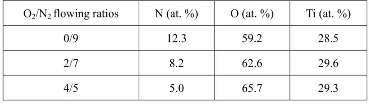
3.2 Composition of TiO2-xNx………43
3.3 Thickness of Different Power………....47
3.4 The Relation between Absorption to Band Gap of TiO2-xNx………...52
3.5 The Water Contact Angle………...…59
3.6 Roughness Effects The Water Contact Angle………....66
3.7 Intensity of Light Effects The Water Contact Angle………....71
3.8 The Absorption on Different Bases of PET and Glass……….…72
3.9 The effect of Sputter’s Power and Time for Absorption………..80
Chapter 4 Conclusions………....…………..…84
References………..……….…….….86
Vita………..………….….……….90
Figure Captions
Chapter 1
Figure 1-1 The unit cell of rutile……….….5
Figure 1-2 The crystal structure of rutile………...6
Figure 1-3 Ball-and-stick model of anatase's unit cell………8
Figure 1-4 The crystal structure of anatase………..9
Figure 1-5 Image from a video contact angle device which water drops on glass………...……..11
Figure 1-6 Chemical structure of polyethylene terephthalate…………...…….17
Figure 1-7 Light absortion spectrum of polyethylene terephthalate measured using a light spectrophotometer………...……17
Figure 1-8 XRD patterns of N-doped TiO2 films deposited with NH3 flow rate of 150 sccm before and after annealing………...22
Figure 1-9 UV-visible absorption spectra of anatase and rutile TiO2 nanoparticles in water………..22
Figure 1-10 N 1s XPS spectra of TiO2-xNx and TiO2 powders………..23
Figure 1-11 N 1 s X-ray photoelectron spectra of TiO2-xNx (upper trace) and TiO2 powders (lower trace)……….…24
Figure 1-12 XPS spectra of N-doped TiO2 films deposited with NH3 flow rate of 150 sccm: N 1s respectively………...…….25
Figure 1-13. A): UV/Vis diffuse reflectance spectra of the samples. B): Plot of the modified Kubelka–Munk function versus the photon energy of the samples. (a) After doping with nitrogen. (b) Commercial UV photocatalyst. Doping conditions: 10 min at 873 K under a stream of ammonia gas………..….26
Figure 1-14 Models of the energy band gap structure of TiO2-xNx for response
in the visible-light region……….27 Figure 1-15 Water contact angle of N-doped TiO2 films as a function of
visible- or UV-light irradiation time………..…..28
Chapter 2
Figure 2-1 The illustration of our solution for TiO2-XNX preparation flow…...30
Figure 2-2 The illustration of our experiment flow………...…32 Figure 2-3 Block diagram of atomic force microscope……….34 Figure 2-4 Image of contact angle goniometer system………..…37
Chapter 3
Figure 3-1 XRD profiles of the TiO2-XNX thin film which conditions of power
and treatment time are the same and no substrate temperature…...40 Figure 3-2 XRD profiles of the TiO2-XNX thin film which conditions of
treatment time and gas are the same and no substrate
temperature……….……….40 Figure 3-3 XRD profiles of the TiO2-XNX thin film which conditions of power
and treatment time are the same after 500°C annealing and no
substrate temperature……….……..41 Figure 3-4 XRD profiles of the TiO2-XNX thin film which conditions of
treatment time and gas are the same after 500°C annealing and no substrate temperature……….………..41 Figure 3-5 Raman profiles of the TiO2-XNX thin film before annealing and no
substrate temperature……….……..42
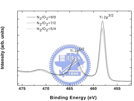
Figure 3-6 XPS spectra of Ti 2p peaks of the TiO2-XNX thin film deposited by
100W power supply for 60min sputtering time and no substrate temperature………..44 Figure 3-7 XPS spectra of O 1s peaks of the TiO2-XNX thin film deposited by
100W power supply for 60min sputtering time and no substrate temperature……….….45 Figure 3-8 XPS spectra of N 1s peaks of the TiO2-XNX thin film deposited by
100W power supply for 60min sputtering time and no substrate temperature………..45 Figure 3-9 SEM images of the TiO2-xNx thin film deposited by 60min
sputtering time and N2/O2=7/2 flow rate with (a) 20W (b) 40W
power supply………..……….48 Figure 3-10 SEM images of the TiO2-xNx thin film deposited by 60min
sputtering time and N2/O2=7/2 flow rate with (a) 60W (b) 80W
power supply………...….49 Figure 3-11 SEM images of the TiO2-xNx thin film deposited by 60min
sputtering time and N2/O2=7/2 flow rate with (a) 100W (b) 120W
power supply………..……..50 Figure 3-12 Top view image of the TiO2-xNx thin film………..51
Figure 3-13 UV-visible absorption spectra of the TiO2-xNx thin film deposited
by 60min sputtering time and N2/O2=6.5/6.0 flow rate with various
power supply………...…….54 Figure 3-14 Plots of the square root of the Kubelka-Munk function against the
photon energy of the TiO2-xNx thin film deposited by 60min
sputtering time and N2/O2=6.5/6.0 flow rate with various power
supply……….……..54
Figure 3-15 UV-visible absorption spectra of the TiO2-xNx thin film deposited
by 60min sputtering time and N2/O2=7/2 flow rate with various
power supply………..……..55 Figure 3-16 Plots of the square root of the Kubelka-Munk function against the
photon energy of the TiO2-xNx thin film deposited by 60min
sputtering time and N2/O2=7/2 flow rate with various power
supply………...55 Figure 3-17 UV-visible absorption spectra of the TiO2-xNx thin film deposited
by 60min sputtering time and N2/O2=9/0 flow rate with various
power supply………...….56 Figure 3-18 Plots of the square root of the Kubelka-Munk function against the
photon energy of the TiO2-xNx thin film deposited by 60min
sputtering time and N2/O2=9/0 flow rate with various power
supply……….………..56 Figure 3-19 UV-visible absorption spectra of the TiO2-xNx thin film deposited
by 90min sputtering time and N2/O2=9/0 flow rate with various
power supply………...….57 Figure 3-20 Plots of the square root of the Kubelka-Munk function against the
photon energy of the TiO2-xNx thin film deposited by 90min
sputtering time and N2/O2=9/0 flow rate with various power
supply………...57 Figure 3-21 Plots of the square root of the Kubelka-Munk function against the
photon energy of the TiO2-xNx thin film deposited by 60min
sputtering time and 100W power supply with different ratio of
N2/O2………....58
Figure 3-22 Water contact angle images of the TiO2-xNx thin film deposited by XIII
40W sputtering for 60min with N2/O2=6.5/6.0 flow rate upon
UV-light illumination………..….61 Figure 3-23 Water contact angle profiles of the TiO2-xNx thin film deposited by
20W sputtering for 60 min with various x………...62 Figure 3-24 Water contact angle profiles of the TiO2-xNx thin film deposited by
40W sputtering for 60 min with various x……….…..62 Figure 3-25 Water contact angle profiles of the TiO2-xNx thin film deposited by
60W sputtering for 60 min with various x……….…..63 Figure 3-26 Water contact angle profiles of the TiO2-xNx thin film deposited by
80W sputtering for 60 min with various x………...……63 Figure 3-27 Water contact angle profiles of the TiO2-xNx thin film deposited by
100W sputtering for 60 min with various x……….64 Figure 3-28 Water contact angle profiles of the TiO2-xNx thin film deposited by
120W sputtering for 60 min with various x……….64 Figure 3-29 Water contact angle profiles of the TiO2-xNx thin film upon
UV-VIS light illumination………...……65 Figure 3-30 The effect of extra Ar plasma for water contact angle of the
TiO2-xNx thin film deposited by 100W power sputtering for 90min
with N2/O2=9/0 flow rate……….67
Figure 3-31 Roughness of the TiO2-xNx thin film deposited by 100W sputtering
for 90min with N2/O2=9/0 flow rate with extra Ar plasma
treatment………..…67 Figure 3-32 Roughness of the TiO2-xNx thin film deposited by 100W sputtering
for 90min with N2/O2=9/0 flow rate without extra Ar plasma
treatment………..…68 Figure 3-33 3D AFM images of the TiO2-xNx thin film deposited by 100W
sputtering for 90min with N2/O2=9/0 flow rate with extra Ar plasma
treatment………..68 Figure 3-34 3D AFM images of the TiO2-xNx thin film deposited by 100W
sputtering for 90min with N2/O2=9/0 flow rate without extra Ar
plasma treatment………..…69 Figure 3-35 The effect of roughness for the water contact angle of the TiO2-xNx
thin film deposited with the same conditions……….……….69 Figure 3-36 Roughness of another TiO2-xNx thin film deposited by 100W
sputtering for 90min with N2/O2=9/0 flow rate without extra Ar
plasma………..70 Figure 3-37 The TiO2-xNx thin film illuminated upon different light
intensity………71 Figure 3-38 UV-visible absorption spectra of the TiO2-xNx thin film deposited
on basis of glass by 90min sputtering time and N2/O2=9/0 flow rate
with various power supply………...73 Figure 3-39 UV-visible absorption spectra of the TiO2-xNx thin film deposited
on basis of glass and PET by 90min sputtering time and N2/O2=9/0
flow rate with 60W power supply………...74 Figure 3-40 UV-visible absorption spectra of the TiO2-xNx thin film deposited
on basis of glass and PET by 90min sputtering time and N2/O2=9/0
flow rate with 80W power supply………...74 Figure 3-41 UV-visible absorption spectra of the TiO2-xNx thin film deposited
on basis of glass and PET by 90min sputtering time and N2/O2=9/0
flow rate with 100W power supply……….…75 Figure 3-42 UV-visible absorption spectra of the TiO2-xNx thin film deposited
on basis of glass and PET by 90min sputtering time and N2/O2=9/0 XV
flow rate with 120W power supply……….75 Figure 3-43 UV-visible absorption spectra of the TiO2-xNx thin film deposited
on basis of glass and PET by 90min sputtering time and N2/O2=9/0
flow rate with 120W power supply at UV region………...….76 Figure 3-44 Water contact angle images of the TiO2-xNx thin film deposited by
120W sputtering for 90min with N2/O2=9/0 flow rate upon UV-light
illumination………..…76 Figure 3-45 UV-visible absorption spectra of the TiO2-xNx thin film deposited
on basis of glass and PET by 90min sputtering time and N2/O2=9/0
flow rate with 120W power supply at visible region…………..….77 Figure 3-46 Water contact angle images of the TiO2-xNx thin film deposited by
120W sputtering for 90min with N2/O2=9/0 flow rate upon
visible-light illumination……….77 Figure 3-47 Water contact angle images of the TiO2-xNx thin film deposited on
bases of PET and glass………78 Figure 3-48 The roughness of the TiO2-xNx thin film deposited on base of
PET……….78 Figure 3-49 The roughness of the TiO2-xNx thin film deposited on base of
glass……….79 Figure 3-50 UV-visible absorption spectra of the TiO2-xNx thin film deposited
by 100W sputtering power supply and N2/O2=7/2 flow rate with
various time……….81 Figure 3-51 SEM images of the TiO2-xNx thin film deposited by 60min
sputtering time and N2/O2=7/2 flow rate with 120W power
supply………..81 Figure 3-52 SEM images of the TiO2-xNx thin film deposited by 70min
sputtering time and N2/O2=7/2 flow rate with 100W power
supply………...……82 Figure 3-53 SEM images of the TiO2-xNx thin film deposited by 60min
sputtering time and N2/O2=7/2 flow rate with 100W power
supply………...…82 Figure 3-54 UV-visible absorption spectra of the TiO2-xNx thin film deposited
through N2/O2=7/2 flow rate with various time and power supply in
order to get the same thickness………...….83
Table Captions
Table 1-1 Properties of PET……….…….18 Table 2-1 Established types of scanning probe microscopy……….……….…35 Table 3-1 The composition of the TiO2-xNx thin films with no substrate
temperature………...………...46 Table 3-2 Growth rate of the TiO2-xNx thin film with various power…. ……..51
Chapter 1 Introduction
1.1 Introduction of TiO
2The discovery of the super-hydrophilicity on TiO2 thin film surface has
prompted extensive research on TiO2 and other semiconductor materials such as
ZnO, Ta2O5, In2O3, InTaO4 or indium-tin oxides (ITO), which has been widely
adopted as an important substance for solar energy conversion and environmental purification. Although various semiconductors have been studied, TiO2 is known to
be one of the most efficient and stable photocatalysts with respect to air or water purification and energy renewal. Its application spreads a wide variety of photochemical reaction, including used in photo-electrolysis, and solar cells. It was found out that the TiO2 surface became slightly hydrophilic under UV irradiation.
This wettability is originated in photo-generated holes produced in TiO2. This highly
hydrophilic phenomenon has been applied in various industrial items such as self-cleaning, exterior tiles, and antifogging mirrors. These applications have been limited to outdoor use only, as the super-hydrophilic conversion requires UV light irradiation of approximately the intensity as natural sunlight. The development of photo-induced sensitive in visual light irradiation condition is very important for indoor use. This photo-induced surface wettability conversion phenomenon has further aroused people’s research interest in TiO2, which will potentially an
important role in environmental purification and solar energy conversion. Several approaches have been used to modify the TiO2 for use in visible light. The main
researches were doping transition metal into TiO2, fabricating reduced TiO2-x
photocatalyst and substituted nitrogen, carbon or sulfur to oxygen in TiO2. However,
doped materials suffer from a thermal instability, an increase of carrier-recombination centers, or the requirement of an expensive ion-implantation
facility. Asahi have calculated densities of states (DOSs) of the substitutional doping of C, N, F, P, or S for O in the anatase TiO2 crystal, by the full potential liberalized
augmented plane wave formalism in the framework of the local density approximation. The substitutional doping of N was the most effective because its P states contribute to the band-gap narrowing by mixing with O 2p states.
1. 2 Material Groups and Structure of TiO
2 [22] [23]Titanium dioxide
Titanium dioxide, also known as titanium(IV) oxide or titania, is the naturally occurring oxide of titanium, chemical formula TiO2.
Natural occurrence
Titanium dioxide occurs in four forms:
z rutile, a tetragonal mineral usually of prismatic habit, often twinned; z anatase or octahedrite, a tetragonal mineral of dipyramidal habit;
z brookite, an orthorhombic mineral. Both anatase and brookite are relatively rare minerals;
z Titanium dioxide (B) or TiO2(B), a monoclinic mineral.
z Titanium Oxide or TiO, as present in K and M spectral type stars.
Titanium dioxide occurrences in nature are never pure; it is found with contaminant metals such as iron. The oxides can be mined and serve as a source for commercial titanium. The metal can also be mined from other minerals such as ilmenite or leucoxene ores, or one of the purest forms, rutile beach sand.
z Rutile
Rutile is a mineral composed primarily of titanium dioxide, TiO2.Rutile is the
most common natural form of TiO2, with two rarer polymorphs anatase (sometimes 2
known by the obsolete name 'octahedrite'), a tetragonal mineral of pseudo-octahedral habit; and brookite, an orthorhombic mineral.
Rutile has among the highest refractive indices of any known mineral and also exhibits high dispersion. Natural rutile may contain up to 10% iron and significant amounts of niobium and tantalum.
Rutile derives its name from the Latin rutilus, red, in reference to the deep red color observed in some specimens when viewed by transmitted light.
Occurrence :
Rutile is a common accessory mineral in high-temperature and high-pressure metamorphic rocks and in igneous rocks.
Rutile is the preferred polymorph of TiO2 in such environments because it has
the lowest molecular volume of the three polymorphs; it is thus the primary titanium bearing phase in most high pressure metamorphic rocks, chiefly eclogites. Brookite and anatase are typical polymorphs of rutile formed by retrogression of metamorphic rutile.
Within the igneous environment, rutile is a common accessory mineral in plutonic igneous rocks, although it is also found occasionally in extrusive igneous rocks, particularly those which have deep mantle sources such as kimberlites and lamproites. Anatase and brookite are found in the igneous environment particularly as products autogenic alteration during the cooling of plutonic rocks; anatase is also found formed within placer deposits sourced from primary rutile.
The occurrence of large specimen crystals is most common in pegmatites, skarns and particularly granite greisens.
Rutile is found as an accessory mineral in some altered igneous rocks, and in certain gneisses and schists. In groups of acicular crystals it is frequently seen penetrating quartz as in the "fléches d'amour" from Grisons, Switzerland.
Uses and economic importance:
Rutile, when present in large enough quantities in beach sands, forms an important constituent of heavy mineral sands ore deposits. It is primarily extracted for use in refractory manufacture or use as a base for paints. Rarely is it extracted as an ore of titanium.
Finely powdered rutile is a brilliant white pigment and is used in paints, plastics, papers, foods, and other applications that call for a bright white color. Titanium dioxide pigment is the single greatest use of titanium worldwide. Nanoscale particles of rutile are transparent to optical light but remain highly reflective to UV light. Hence, they are used in sunscreens.
Small rutile needles present in gems are responsible for an optical phenomenon known as asterism. Asteriated gems are known as "star" gems. Star sapphires, star rubies, and other "star" gems are highly sought after and often more valuable than their normal equivalents.
Synthetic rutile
Synthetic rutile was first produced in 1948 and is sold under a variety of names. Very pure synthetic rutile is transparent and almost colorless (slightly yellow) in large pieces. Synthetic rutile can be made in a variety of colors by doping, although the purest material is almost colorless. The high refractive index gives an adamantine lustre and strong refraction that leads to a diamond-like appearance. The
near-colorless diamond substitute is sold under the name Titania, which is the old-fashioned chemical name for this oxide. However, rutile is seldom used in jewellery because it is not very hard (scratch-resistant), measuring only about 6 on the Mohs hardness scale.
Figure 1-1 The unit cell of rutile
Figure 1-2 The crystal structure of rutile .
z Anatase[24]
Anatase is one of the three mineral forms of titanium dioxide (the other two being brookite and rutile). It is always found as small, isolated and sharply developed crystals, and like rutile, a more commonly occurring modification of titanium dioxide, it crystallizes in the tetragonal system; but, although the degree of symmetry is the same for both, there is no relation between the interfacial angles of the two minerals, except, of course, in the prism-zone of 45° and 90°. The common pyramid of anatase, parallel to the faces of which there are perfect cleavages, has an angle over the polar edge of 82°9', the corresponding angle of rutile being 56°52½'It was on account of this steeper pyramid of anatase that the mineral was named, by RJ Haüy in 1801, from the Greek anatasis, "extension," the vertical axis of the crystals being longer than in rutile. There are also important differences between the physical characters of anatase and rutile; the former is not quite so hard (H=5½-6) or dense
(specific gravity 3.9); it is optically negative, rutile being positive; and its lustre is even more strongly adamantine or metallic-adamantine than that of rutile.
Two types or habits of anatase crystals may be distinguished. The commoner occurs as simple acute double pyramids with an indigo-blue to black colour and steely lustre. Crystals of this kind are abundant at Le Bourg-d'Oisans in Dauphiné, where they are associated with rock-crystal, feldspar, and axinite in crevices in granite and mica-schist. Similar crystals, but of microscopic size, are widely distributed in sedimentary rocks, such as sandstones, clays, and slates, from which they may be separated by washing away the lighter constituents of the powdered rock.
Crystals of the second type have numerous pyramidal faces developed, and they are usually flatter or sometimes prismatic in habit; the colour is honey-yellow to brown. Such crystals closely resemble xenotime in appearance and, indeed, were for a long time supposed to belong to this species, the special name wiserine being applied to them. They occur attached to the walls of crevices in the gneisses of the Alps, the Binnenthal near Brig in canton Valais, Switzerland, being a well-known locality.
When strongly heated, anatase is converted into rutile, changing in specific gravity to 4.1; naturally occurring pseudomorphs of rutile after anatase are also known. Crystals of anatase have and continue to be artificially prepared in laboratories by introducing the moisture-sensitive titanium tetrachloride, TiCl4, to
water at very cold temperatures (the process is very exothermic) to produce TiO2 and
HCl gas. Such synthetic forms of anatase are currently under scrutiny in the field of semiconductors and photovoltaic materials.
Another name commonly in use for this mineral is octahedrite, a name which, indeed, is earlier than anatase, and given because of the common (acute) octahedral habit of the crystals. Other names, now obsolete, are oisanite and dauphinite, from the well-known French locality.
Figure 1-3 Ball-and-stick model of anatase's unit cell
Figure 1-4 The crystal structure of anatase .
z Brookite
Brookite is a mineral consisting of titanium oxide, TiO2, and hence identical
with rutile and anatase in composition, but crystallizing in the orthorhombic system (see crystal structure).
It was named for Henry James Brooke, English mineralogist, 1771 - 1857.
z Titanium dioxide (B) [25] [26] [27] [28]
Titanium dioxide (B) or TiO2(B) is the monoclinic form of titanium dioxide.
The mineral is found in weathering rims on tektites and perovskite and as lamellae in
anatase from hydrothermal veins and has a density lower than that of the other three polymorphs.
In the laboratory anatase can be converted in a hydrothermal route to TiO2(B)
nanotubes and nanowires which are of potential interest as catalytic supports and photocatalysts. For this to happen anatase is mixed with 15M sodium hydroxide and heated at 150 ° C for 72 hours. The reaction product is washed with dilute hydrochloric acid and heated at 400 °C for another 15 hours. the yield of nanotubes is quantitative and the tubes have an outer diameter of 10 to 20 nanometres and an inner diameter of 5 to 8 nanometres and have a length of 1 micrometres. A higher reaction temperature (170 °C) and less reaction volume gives the corresponding nanowires.
1.3 Characteristic of TiO
2-xN
xUV-VIS light absorption
In physics, absorption is the process by which the energy of a photon is taken up by another entity, for example, by an atom whose valence electrons make transition between two electronic energy levels. The photon is destroyed in the process. The absorbed energy may be re-emitted as radiant energy or transformed into heat energy. The absorption of light during wave propagation is often called attenuation.
The absorbance of an object quantifies how much light is absorbed by it. This may be related to other properties of the object through the Beer-Lambert law.
For most substances, the amount of absorption varies with the wavelength of the light, leading to the appearance of colour in pigments that absorb some wavelengths but not others. For example, an object that absorbs blue, green and
yellow light will appear red when viewed under white light. More precise measurements at many wavelengths allow the identification of a substance via absorption spectroscopy.
Contact angle [29][31]
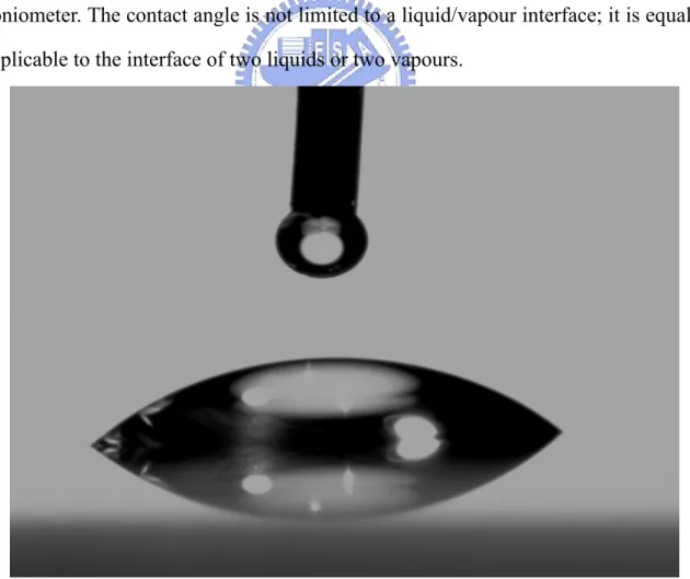
The contact angle is the angle at which a liquid/vapor interface meets the solid surface. The contact angle is specific for any given system and is determined by the interactions across the three interfaces. Most often the concept is illustrated with a small liquid droplet resting on a flat horizontal solid surface. The shape of the droplet is determined by the Young-Laplace equation. The contact angle plays the role of a boundary condition. Contact angle is measured using a contact angle goniometer. The contact angle is not limited to a liquid/vapour interface; it is equally applicable to the interface of two liquids or two vapours.
Figure 1-5 Image from a video contact angle device which water drops on glass.
In near years , the other people report about the change in water contact angle on
semiconductor oxides such as ZnO, Ta2O5, In2O3, InTaO4 or indium–tin oxides (ITO) and the unexpected response of some of them to irradiation with visible light. TiO2 has been used as a reference material. These oxides are known because they present some kind of photoactivity and have band gaps within the UV region of the spectrum. Except for ZnO, no results about hydrophilic adjustment of contact angles upon light irradiation have been reported for the other investigated oxides. Meanwhile, for InTaO4 it has been reported recently that this photoactive material doped with nickel is able to split the water into H2 and O2 when irradiated with visible light .
Wetting [30]
Wetting is the contact between a fluid and a surface, when the two are brought into contact. When a liquid has a high surface tension (strong internal bonds), it will form a droplet, whereas a liquid with low surface tension will spread out over a greater area (bonding to the surface). On the other hand, if a surface has a high surface energy (or surface tension), a drop will spread, or wet, the surface. If the surface has a low surface energy, a droplet will form. This phenomenon is a result of the minimization of interfacial energy. If the surface is high energy, it will want to be covered with a liquid because this interface will lower its energy, and so on.
The primary measurement to determine wettability is a contact angle measurement. This measures the angle between the surface and the surface of a liquid droplet on the surface. For example, a droplet would have a high contact angle, but a liquid spread on the surface would have a small one. The contact angle and the surface energies of the materials involved are related by the Young–Dupré equation
where is the surface tension between two substances and S, V, and L correspond to the solid, vapor, and liquid substances in a contact angle experiment respectively.
A contact angle of 90° or greater generally characterizes a surface as not-wettable, and one less than 90° means that the surface is wettable. In the context of water, a wettable surface may also be termed hydrophilic and a non-wettable
surface hydrophobic. Superhydrophobic surfaces have contact angles greater than 150°, showing almost no contact between the liquid drop and the surface. This is sometimes referred to as the "Lotus effect". This characteristic of spreading out over a greater area is sometimes called 'wetting action' when discussing solders and soldering.
Wetting is often an important factor in the bonding (adherence) of two materials. It is also the basis for capillary action, the ability of a narrow tube to draw a liquid, even against the force of gravity.
Hydrophile
Hydrophile, from the Greek (hydros) "water" and φιλια (philia) "friendship," refers to a physical property of a molecule that can transiently bond with water (H2O)
through hydrogen bonding. This is thermodynamically favorable, and makes these molecules soluble not only in water, but also in other polar solvents. There are hydrophillic and hydrophobic parts of the cell membrane.
A hydrophilic molecule or portion of a molecule is one that is typically charge-polarized and capable of hydrogen bonding, enabling it to dissolve more readily in water than in oil or other hydrophobic solvents. Hydrophilic and hydrophobic molecules are also known as polar molecules and nonpolar molecules, respectively.
Soap has a hydrophilic head and a hydrophobic tail which allows it to dissolve in both waters and oils, therefore allowing the soap to clean a surface.
Super hydrophilicity [32]
Under light irradiation, water dropped onto titanium dioxide forms no contact angle (almost 0 degrees). This effect, called super hydrophilicity, was discovered in 1995. Super hydrophilic material has various advantages. For example, it can defog glass, and it can also enable oil spots to be swept away easily with water. Such
materials are already commercialized as door mirrors for cars, coatings for buildings, etc.
Several mechanisms of this super hydrophilicity have been proposed by researchers. One is the change of the surface structure to a metastable structure, and another is cleaning the surface by the photodecomposition of dirt such as organic compounds adsorbed on the surface, after either of which water molecules can adsorb to the surface. The mechanism is still controversial, and it is too soon to decide which suggestion is correct. To decide, atomic scale measurements and other studies will be necessary.
1.4 Applications of TiO
2 [22] [23]As a pigment of high refringence, titanium dioxide is the most widely used white pigment because of its brightness and very high refractive index (n=2.4), in which it is surpassed only by a few other materials. When deposited as a thin film, its refractive index and colour make it an excellent reflective optical coating for dielectric mirrors and some gemstones, for example "mystic fire topaz". TiO2 is also an effective
opacifier in powder form, where it is employed as a pigment to provide whiteness and opacity to products such as paints, coatings, plastics, papers, inks, foods, and most toothpastes. Used as a white food coloring, it has E number E171. In cosmetic and skin care products, titanium dioxide is used both as a pigment and a thickener. It is also used as a tattoo pigment and styptic pencils.
This pigment is used extensively in plastics and other applications for its UV resistant properties where it acts as a UV reflector.
In ceramic glazes titanium dioxide acts as an opacifier and seeds crystal formation. In almost every sunscreen with a physical blocker, titanium dioxide is
found both because of its refractive index and its resistance to discoloration under ultraviolet light. This advantage enhances its stability and ability to protect the skin from ultraviolet light.
Titanium oxide is also used as a semi-conductor.
Photocatalyst
Titanium dioxide, particularly in the anatase form, is a photocatalyst under ultraviolet light. Recently it has been found that titanium dioxide, when spiked with nitrogen ions, is also a photocatalyst under visible light. The strong oxidative potential of the positive holes oxidizes water to create hydroxyl radicals. It can also oxidize oxygen or organic materials directly. Titanium dioxide is thus added to paints, cements, windows, tiles, or other products for sterilizing, deodorizing and anti-fouling properties and is also used as a hydrolysis catalyst. It is also used in the Graetzel cell, a type of chemical solar cell.
Titanium dioxide has potential for use in energy production: as a photocatalyst, it can carry out hydrolysis, i.e., break water into hydrogen and oxygen. Were the hydrogen collected, it could be used as a fuel. The efficiency of this process can be greatly improved by doping the oxide with carbon, as described in "Carbon-doped titanium dioxide is an effective photocatalyst" .
As TiO2 is exposed to UV light, it becomes increasingly hydrophilic; thus, it can
be used for anti-fogging coatings or self-cleaning windows. TiO2 incorporated into
outdoor building materials can substantially reduce concentrations of airborne pollutants such as volatile organic compounds and nitrogen oxides.
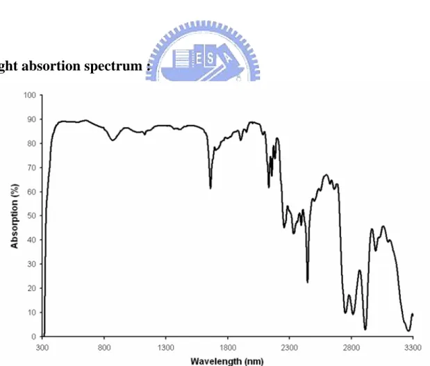
1.5 Polyethylene Terephthalate
[33] 1.5.1 IntroductionPolyethylene terephthalate (aka PET, PETE or the obsolete PETP or PET-P) is a thermoplastic polymer resin of the polyester family that produced by the chemical industry and is used in synthetic fibers; beverage, food and other liquid containers; thermoforming applications; and engineering resins often in combination with glass fiber. It is one of the most important raw materials used in man-made fibers.
Depending on its processing and thermal history, it may exist both as an amorphous (transparent) and as a semi-crystalline (opaque and white) material. Its monomer can be synthesized by the esterification reaction between terephthalic acid and ethylene glycol with water as a byproduct or the transesterification reaction between ethylene glycol and dimethyl terephthalate with methanol as a byproduct. Polymerization is through a polycondensation reaction of the monomers (done immediately after esterification/transesterification) with ethylene glycol as the byproduct (the ethylene glycol is recycled in production).
The majority of the world's PET production is for synthetic fibers (in excess of 60%) with bottle production accounting for around 30% of global demand. In discussing textile applications, PET is generally referred to as simply "polyester" while "PET" is used most often to refer to packaging applications.
Chemical structure :
Figure 1-6 Chemical structure of polyethylene terephthalate.
Light absortion spectrum :
Figure 1-7 Light absortion spectrum of polyethylene terephthalate measured using a light spectrophotometer .
Table 1-1 Properties of PET.
[33]
PET
Density 1370 kg/m3
Young modulus(E) 2800–3100 MPa
Tensile strength(σt) 55–75 MPa
Elongation @ break 50–150% notch test 3.6 kJ/m2 Glass temperature 75 °C melting point 260 °C Vicat B 170 °C Thermal conductivity 0.24 W/m.K
linear expansion coefficient (α) 7×10⁻⁵/K
Specific heat (c) 1.0 kJ/kg.K
Water absorption (ASTM) 0.16
Price 0.5–1.25 €/kg
1.5.2 Crystals
Crystallization occurs when polymer chains fold up on themselves in a repeating, symmetrical pattern. Long polymer chains tend to become entangled on themselves, which prevents full crystallization in all but the most carefully controlled circumstances. PET is no exception to this rule; 60% crystallization is the upper limit for commercial products, with the exception of polyester fibers.
PET in its natural state is a crystalline resin. Clear products can be produced by rapidly cooling molten polymer to form an amorphous solid. Like glass, amorphous PET forms when its molecules are not given enough time to arrange themselves in an orderly fashion as the melt is cooled. At room temperature the molecules are frozen in place, but if enough heat energy is put back into them, they begin to move again, allowing crystals to nucleate and grow. This procedure is known as solid-state crystallization.
Like most materials, PET tends to produce many small crystallites when crystallized from an amorphous solid, rather than forming one large single crystal. Light tends to scatter as it crosses the boundaries between crystallites and the amorphous regions between them. This scattering means that crystalline PET is opaque and white in most cases. Fiber drawing is among the few industrial processes that produces a nearly single-crystal product.
1.5.3 Applications
PET can be semi-rigid to rigid, depending on its thickness, and is very lightweight. It makes a good gas and fair moisture barrier, as well as a good barrier to alcohol (requires additional "Barrier" treatment) and solvents. It is strong and impact-resistant. It is naturally colorless and transparent.
When produced as a thin film (often known by the tradename Mylar), PET is often
coated with aluminium to reduce its permeability, and to make it reflective and opaque. PET bottles are excellent barrier materials and are widely used for soft drinks, (see carbonation). PET or Dacron is also used as a thermal insulation layer on the outside of the International Space Station as seen in an episode of Modern Marvels "Sub Zero". For certain specialty bottles, PET sandwiches an additional polyvinyl alcohol to further reduce its oxygen permeability.
When filled with glass particles or fibers, it becomes significantly stiffer and more durable. This glass-filled plastic, in a semi-crystalline formulation, is sold under the tradename Rynite.
While all thermoplastics are technically recyclable, PET bottle recycling is more practical than many other plastic applications. The primary reason is that plastic carbonated soft drink bottles and water bottles are almost exclusively PET which makes them more easily identifiable in a recycle stream. PET has a resin identification code of 1. PET, as with many plastics, is also an excellent candidate for thermal recycling (incineration) as it is composed of carbon, hydrogen and oxygen with only trace amounts of catalyst elements (no sulfur) and has the energy content of soft coal.
PET was patented in 1941 by the Calico Printers' Association of Manchester. The PET bottle was patented in 1973.
1.6 Review
1.6.1 XRD patterns of N-doped TiO2
X-ray diffraction patterns of the N-doped TiO2 films deposited with NH3 flow
rate of 150 sccm before and after annealing are shown in Fig. 1-8. The as-grown film does not show any diffraction peaks. After annealing, the crystalline phase of anatase is found in the 400°C annealed film, both anatase and rutile phases in the 600°C annealed film, and the rutile phase in the 900°C annealed film, respectively. Similar results are obtained in the films deposited by changing NH3 flow rate. In the undoped
TiO2 films, only anatase phase is observed after 600°C annealing. Because the
intermingled structure of anatase and rutile phases is formed in the N-doped TiO2
films annealed at 600°C, it is found that the transition temperature from anatase to rutile becomes lower by nitrogen doping [11]. To evaluate the effect of UV-visible absorption performance on photocatalytic activity of the nanoparticles, UV-visible absorption spectra of anatase and rutile TiO2 nanoparticles in water were measured in
Fig. 1-9. Clearly, absorption and scattering of anatase TiO2 nanoparticles are stronger
than those of rutile TiO2, which guarantees the relatively high photocatalytic activity
of the former [17].
Figure 1-8 XRD patterns of N-doped TiO2 films deposited with NH3 flow rate of 150 sccm
before and after annealing.
Figure 1-9 UV-visible absorption spectra of anatase and rutile TiO2 nanoparticles in water.
1.6.2 XPS patterns of N-doped TiO2
Fig. 1-10 shows the N 1s XPS spectra of TiO2-xNx and TiO2 powders. Since peaks
at 396 eV, which have previously been found to result from Ti-N bonds, are observed for the powders annealed under NH3, it was determined that the oxygen sites were substituted by nitrogen atoms. Since the XRD did not indicate the formation of TiN bonds, it was determined that O-Ti-N bonds formed. Therefore, these powders were described as TiO2-xNx. In contrast, the air-annealed samples did not display a peak at
396 eV and is TiO2. The peak around 400 eV is the chemisorbed N2 molecule, which
absorbs onto the surface. While the N 1 s X-ray photoelectron spectrum of TiO2-xNx
shown in Fig. 1-11 features a peak at 399.95 eV, known to be attributable to adsorbed NO or N in Ti-O-N, no weak peak attributable to Ti-N bonding can be seen at 396 eV due to the noise, as shown in the upper trace in Fig. 1-11. In the case of undoped TiO2
powder, neither peak is observed, as shown in the lower trace in Fig. 1-11[13].
Figure 1-10 N 1s XPS spectra of TiO2-xNx and TiO2 powders.
Figure 1-11 N 1 s X-ray photoelectron spectra of TiO2-xNx (upper trace) and TiO2
powders (lower trace).
XPS spectra of the N-doped TiO2 film deposited with NH3 flow rate of 150 sccm
are shown in Fig. 1-12 for Ti 2p, b for O 1s, and c for N 1s electrons, respectively. The binding energy of Ti 2p at 459.1 eV shifting from 454 eV of metallic Ti is the signal of Ti in TiO2, and that of O 1s at 531 eV is assigned to metallic oxide. For N 1s electrons,
two bonding states of nitrogen atoms are observed whose binding energies are 396.1 and 399.3 eV, and these are assigned to the nitrogen atoms substituting for the oxygen atoms (Nsub) and those existing interstitially in the TiO2 matrices (Nint), respectively.
Nsub:Nint ratio estimated from the spectrum intensities becomes about 80:20 [11].
Figure 1-12 XPS spectra of N-doped TiO2 films deposited with NH3 flow rate of 150 sccm: N
1s respectively.
1.6.3 Absorption and energy band gap
In the case of Si- TiO2-xNx films, the crystalline forms before and after doping
with nitrogen were characterized as being of anatase-type, with a crystalline size of 11 nm. Fig. 1-13(A) shows a comparison of the UV/Vis diffuse reflectance spectra of TiO2-xNx and undoped TiO2. The prepared TiO2-xNx photocatalysts, in the form of
powders or thin films, were very vivid yellow in color, and showed a shift to longer wavelengths in accordance with color. Fig. 1-13(B) shows plots of the modified Kubelka–Munk function versus the photon energy, from which the band-gap energies can be obtained. The band-gap energy for TiO2-xNx can be seen to be 2.95 eV,
corresponding to the visible-light region, whereas that for undoped TiO2 is 3.2 eV.
Figure 1-13. A): UV/Vis diffuse reflectance spectra of the samples. B): Plot of the modified Kubelka–Munk function versus the photon energy of the samples. (a) After doping with nitrogen. (b) Commercial UV photocatalyst. Doping conditions: 10 min at 873 K under a stream of ammonia gas.
Fig. 1-14(a) shows the band-gap energy structure of the anatase-type UV-driven photocatalyst, while Fig. 1-14(b), reported by Asahi et al., shows the narrowed band-gap structure obtained by mixing of N 2p and O 2p orbit. Fig. 1-14(c), reported by Nakamura et al., shows the midgap energy level formed slightly above the valence band. The schemes represented in Figure 1-14(b) and (c) are both used in engineering for visible-light-driven photocatalyst materials. Mechanisms to achieve responsiveness to visible light are still under investigation, and no complete interpretation has yet been formulated. Thus, the mechanisms of reactions of specific compounds with TiO2-xNx
may help in delineating the mechanistic aspects of reactivity in the visible-light region
[13].
Figure 1-14. Models of the energy band gap structure of TiO2-xNx for response in the
visible-light region.
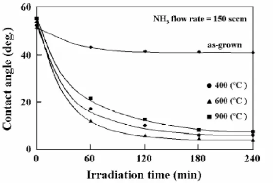
1.6.4 Water contact angle
Photo-induced hydrophilicity after the visible-light irradiation was evaluated by measuring the contact angle of water on the film surface. The contact angle of
as-grown and annealed N-doped TiO2 films deposited using NH3 flow rates of 150
sccm as a function of visible-light irradiation time is shown in Fig. 1-15. It is found that weak photo-induced hydrophilicity for visible-light irradiation is observed even in the as-grown film. The photo-induced hydrophilicity enhances remarkably when the film is annealed. Higher photo-induced hydrophilicity is also observed in the film with intermingled structure of anatase and rutile [11]. All of these experiments heat the substrate for a high temperature.
Figure 1-15. Water contact angle of N-doped TiO2 films as a function of visible- or UV-light
irradiation time.
Chapter 2 Experiment Details
2.1 System of Radio-Frequency Magnetron Sputter
Sputtering system has been widely used to deposit various metal films in ULSI fabrication, and it was also used to deposit dielectrics because of its easy-control and low cost. In the experiment, the thin films were deposited by a single target radio-frequency (RF) magnetron sputtering system. The sputtering system is composed of several parts including
(a) Gas flow controlling system: In general, the percentage of oxygen in the sputtering atmosphere played an important role in oxide ceramics. We used Gas MFC (mass flow meter) to control the flow rate and atmosphere contents during the sputtering process. So we could find out that the dependence of the mass ratio for the device performance by tuning recipe
(b) Mechanical modules: vacuum chamber, targets, and shutter. In addition, a DC motor to let the thin films grow uniformly controlled the rotational substrate holder.
(c) Vacuum pump modules: a diffusion pump (high vacuum pump) and one mechanical pump (low vacuum pump). The chamber base pressure was evacuated to 3×10⁻⁵ torr prior to the thin film deposition.
(d) RF power modules: the RF power generator (13.56 MHz) was controlled by a RF power supply with an automatic matching network, which can be tuned to minimum reflected power.
(e) Pressure modules: pressure gauges, exhaust valves, gas supply, and mass flow controllers. Pure gas was introduced by mass flow controllers after the system was evacuated to base pressure. Pressure modules and vacuum pump modules control the working pressure.
(f) Cooling system: There was cooling water that flows in the pipe welded on the chamber and in the magnetron gun. During the sputtering process, the heating lamps and plasma always produced a lot of redundant heat energy in the chamber. We needed cooling water to prevent from mechanical breakdown and maintain the sample uniformity.
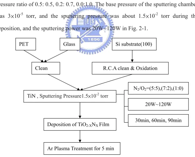
2.2 Thin Films Preparation by Sputter
TiO2 films were deposited on PET substrates by RF(13.56 MHz) sputtering
method without heating. The sputtered target was TiN (2 inches) with a purity of 99.999%, the distance between the target and the substrate was about 30 mm. The sputtering and reactive gas was a mixture of oxygen and nitrogen with a partial pressure ratio of 0.5: 0.5, 0.2: 0.7, 0.0:1.0. The base pressure of the sputtering chamber was 3×10⁻⁵ torr, and the sputtering pressure was about 1.5×10⁻² torr during the deposition, and the sputtering power was 20W~120W in Fig. 2-1.
Si substrate(100)
PET Glass
Clean
Deposition of TiO2-XNX Film
N2/O2=(5:5),(7:2),(1:0)
20W~120W TiN , Sputtering Pressure1.5×10-2 torr
30min, 60min, 90min R.C.A clean & Oxidation
Ar Plasma Treatment for 5 min
Figure 2-1 The illustration of our solution for TiO2-XNX preparation flow
2.3 The process of experiment
In our experiment, it can be sorted into sample preparation, optical property analysis, and material analysis, as Fig. 2-2.
There are many aspects of our sample analysis. In the side of material analysis, the microstructure and crystallization analysis, that is realized by the scanning electron microscope system (SEM), X-ray Photoelectron Spectroscopy (XPS), Raman Spectroscopy, the atomic force microscopy (AFM), and the X-ray diffraction system (XRD). In the side of optical property analysis, the photo-induced surface wettability conversion reaction of the thin films was investigated by water contact angle measurement, and the absorbance of TiO2-XNX thin films was measured by
UV-VIS spectrophotometer.
XRD RS
SEM XPS
AFM
Material Analysis Optical Property Analysis
Sample preparation
UV-Vis Spectrophotometer
Water contact angle system
Conduction mechanism analysis
Result and discussion
Modify process
Figure 2-2 The illustration of our experiment flow
2.4 Measurements and Materials Analysis
2.4.1 X-Ray Diffraction (XRD)
The crystal structure of the TiO2-xNx was observed by the X-ray diffraction (XRD,
MAC Science, MXP18, Japan). X-ray diffraction (XRD) was the equipment used for identifying the crystal structure, but the thin film of TiO2-xNx is too thin .If the
included angle θ (Bragg’s angle) between the crystal plane and the incident light matched the Bragg’s law (nλ=2dsinθ) , the incident light was diffracted by the crystal plane .By using Bragg’s law for diffraction , the reflected x-rays from the respective atomic planes can be measured by the detector .In the Bragg’s law ( nλ=2dsinθ) , nλ is an integral number of wavelengths , and d is the distance between two successive crystal planes .
The X-ray diffraction measurement with Cu Kα radiation (λ=1.5418 Å) was operated at 30KV and 20mA. In order to avoid the peak of silicon at about 70°, the angle 2θ of the measurement was from 20° to 60°. The sweeping rate was 4° per minute.
2.4.2 Scanning Probe Microscopy (SPM)
Scanning probe microscopy (SPM) is a branch of microscopy that forms images of surfaces using a physical probe that scans the specimen .An image of the surface is obtained by mechanically moving the probe in a raster scan of the specimen, line by line, and recording the probe-surface interaction as a function of position. SPM was founded with the invention of the scanning tunneling microscope in 1981.
Many scanning probe microscopes can image several interactions simultaneously. The manner of using these interactions to obtain an image is generally called a mode.
Figure 2-3 Block diagram of atomic force microscope.
Advantages of scanning probe microscopy
1. The resolution of the microscopes is not limited by diffraction, but only by the size of the probe-sample interaction volume (i.e., point spread function), which can be as small as a few Pico meter.
2. The interaction can be used to modify the sample to create small structures.
Disadvantages of scanning probe microscopy
1. The scanning techniques are generally slower in acquiring images, due to the scanning process. As a result, efforts are being made to greatly improve the scanning rate.
2. The maximum image size is generally smaller. Table 2-1 Established types of scanning probe microscopy 1. AFM
z Contact AFM z Non-contact AFM z Dynamic contact AFM
Atomic force microscopy
2. EFM Electrostatic force microscope
3. ESTM Electrochemical scanning tunneling microscope
4. FMM force modulation microscopy
5. KPFM Kelvin probe force microscopy
6. MFM Magnetic force microscopy
7. MRFM Magnetic resonance force microscopy
8. NSOM Near-field scanning optical microscopy (or SNOM,
scanning near-field optical microscopy)
9. PSTM Photon scanning tunneling microscopy
10. SECM Scanning electrochemical microscopy
11. SCM Scanning capacitance microscopy
12. SGM Scanning gate microscopy
13. SICM Scanning ion-conductance microscopy
14. SPSM Spin polarized scanning tunneling microscopy
15. SThM Scanning thermal microscopy
16. STM Scanning tunneling microscopy
17. SVM Scanning voltage microscopy
2.4.3 Scanning Electron Microscopy (SEM)
The surface structural and morphology analysis of the TiO2-xNx thin film was
observed by field emission scanning electron microscopy (FE-SEM, Hitachi S-4700I, Japan). The measured pressure was at 2 x 10⁻⁶ Torr. The working voltage was 15K eV. The working current was 10μA.
Comprehensively, the surface morphology issue is also a quite important character compared with the character of bulk for the thin films. We could observe the surface micro-morphology and cross section of our sample by SEM. Besides, the
crystallization of the thin films needed to be investigated directly by XRD analysis. So, we could get enough information to support our illustration. The SEM model is S4700I with high resolution of 15 Å made by Hitachi.
2.4.4 X-ray Photoelectron Spectroscopy (XPS)
The X-ray spectroscopy was used to characterize the binding energy and the composition of the TiO2-xNx thin film. The electron binding energy is influenced by
its chemical surroundings making binding energy suitable for determining chemical states. XPS is a surface-sensitive method because the emitted photoelectrons originate from the upper 0.5~5 nm of the sample, just as Auger electrons do, despite the deeper penetration of the primary X-rays compared to a primary electron beam.
2.4.5 Ultraviolet-Visible Spectrophotometers
AbsorbanceIn spectroscopy, the absorbance A is defined as
where I is the intensity of light at a specified wavelength λ that has passed through a sample (transmitted light intensity) and I0 is the intensity of the light before it enters
the sample or incident light intensity. Absorbance measurements are often carried out in analytical chemistry, since the absorbance of a sample is proportional to the thickness of the sample and the concentration of the absorbing species in the sample, in contrast to the transmittance I / I0 of a sample, which varies exponentially with
thickness and concentration. See the Beer-Lambert law for a more complete discussion. The UV-VIS Spectrophotometer is made in Japan(Hitachi U3010, Japan).
2.4.6 Contact Angle System
This quantity examines the system and is different from other factories card only energy examine single some machine platforms which contact the angle. Full-automatic control, but quantity is examined small to the fragmentation, it is big to the glass base plate of 50×60cm. The quantity exposed to the angle examines not only has generally commonly used static mode, still have a advance mode and recede mode, can reflect that lie between the roughness of the interface. In addition, possess four load different polarity inject syringe of solution, can test for the surface free energy of block to appear to ask in time at the same time. This system can be used for being engaged in the following analysis: (1) Hydrophilic of the membrane and Hydrophobe of the membrane. (2) The surface free energy of membrane assessment. (3) Measuring static contact angle. (4) Measuring dynamic contact angle . (5) Measuring surface and interfacial tension. (6) Using for nano-material, polymer composite material, biomaterial, paint, coating, etc.
Figure 2-4 Image of contact angle goniometer system(KRŰSS GmbH, model GH-100).
2.4.7 Raman Spectroscopy(RS)
Raman spectroscopy is a spectroscopic technique used in condensed matter physics and chemistry to study vibrational, rotational, and other low-frequency modes in a system. It relies on inelastic scattering, or Raman scattering of monochromatic light, usually from a laser in the visible, near infrared, or near ultraviolet range. The laser light interacts with phonons or other excitations in the system, resulting in the energy of the laser photons being shifted up or down. The shift in energy gives information about the phonon modes in the system. Infrared spectroscopy yields similar, but complementary information.
Typically, a sample is illuminated with a laser beam. Light from the illuminated spot is collected with a lens and sent through a monochromator. Wavelengths close to the laser line (due to elastic Rayleigh scattering) are filtered out and those in a certain spectral window away from the laser line are dispersed onto a detector.
Spontaneous Raman scattering is typically very weak, and as a result the main difficulty of Raman spectroscopy is separating the weak inelastically scattered light from the intense Rayleigh scattered laser light. Raman spectrometers typically use holographic diffraction gratings and multiple dispersion stages to achieve a high degree of laser rejection. A photon-counting photo-multiplier tube (PMT) or, more commonly, a CCD camera is used to detect the Raman scattered light. In the past, PMTs were the detectors of choice for dispersive Raman setups, which resulted in long acquisition times. However, the recent uses of CCD detectors have made dispersive Raman spectral acquisition much more rapid.
Raman spectroscopy has a stimulated version, analogous to stimulated emission, called stimulated Raman scattering.
Chapter 3 Results and Discussion
3.1 Crystal of TiO
2-xN
xTiO2-xNx thin films were deposited on PET substrates by sputtering a TiN target
under O2, N2, and Ar gas mixture. The thin films were deposited in plasma of argon,
oxygen, and nitrogen with varying nitrogen content without heating temperature. XRD profiles of TiO2-XNX thin film which conditions of power and treatment time
are the same but the scales of treatment gas different are shown in Fig. 3-1. The deposition conditions used were oxygen flow rate of 0 to 7 sccm and nitrogen flow rate of 9 to 2 sccm, radio-frequency power of 100 W, and no substrate temperature. The as-grown film shows a peak which being indexed to the silicon substrate structure. Fig. 3-2 shows XRD profiles of the TiO2-XNX thin film which conditions of
treatment time and gas are the same but power different. The deposition conditions used were a nitrogen flow rate of 9 sccm, a RF power of 20 to 100 W, and no substrate temperature. The result is the same that shows a peak that have been indexed to the silicon substrate structure. However, we anneal those samples. After 500°C annealing, the crystalline phase of anatase is found in those annealed films. In Fig. 3-3 shows XRD profiles of the TiO2-XNX thin film which conditions of power
and treatment time are the same after 500°C annealing. Our TiO2-XNX thin films that
contain the anatase phase with the many peaks of (101) (004) (003) (200) are similar to the anatase powder samples and films reported in many other works. [11] [14] [21] [35]
[36] In Fig. 3-4 also shows the anatase phase with the many peaks of (004) (003) are
similar to the anatase powder samples and films. In order to be sure that our TiO2-XNX thin film is anatase phase, we also have Raman profiles showing in Fig.
3-5. Our TiO2-XNX thin films contain the anatase phase can be confirmed. Absorption
and scattering of anatase TiO2 nanoparticles are stronger than those of rutile TiO2, 39
which guarantees the relatively high photocatalytic activity of the former. [17] 20 25 30 35 40 In te ns it y (a rb .u n it s ) 2Theta (deg.) 100W 60min N2/O2=9/0 100W 60min N2/O2=8/1 100W 60min N2/O2=7/2 100W 60min N2/O2=6/3 100W 60min N2/O2=5/4 100W 60min N2/O2=4/5 100W 60min N2/O2=3/6 100W 60min N2/O2=2/7 Si
Figure 3-1. XRD profiles of the TiO2-XNX thin film which conditions of power and
treatment time are the same and no substrate temperature.
20 30 40 50 60 In te ns ity (ar b .u nits ) 2Theta (deg.) 20W 90m in N2/O2=9/0 40W 90m in N2/O2=9/0 60W 90m in N2/O2=9/0 80W 90m in N2/O2=9/0 100W 90m in N2/O2=9/0 120W 90m in N2/O2=9/0 S i
Figure 3-2. XRD profiles of the TiO2-XNX thin film which conditions of treatment time and
gas are the same and no substrate temperature.
20 25 30 35 40 45 50 55 60 A(004) A:Anatase A(200) 100W 60m in N2/O2=9/0 100W 60m in N 2/O2=8/1 100W 60m in N 2/O2=7/2 100W 60m in N2/O2=6/4 A(003) A(004) A(101) In te n s ity (a rb .u n its ) 2Theta (deg.) Si
Figure 3-3. XRD profiles of the TiO2-XNX thin film which conditions of power and
treatment time are the same after 500°C annealing and no substrate temperature.
20 25 30 35 40 45 50 55 60 A:Anatase A(004) A(003) 120W 90m in N 2/O2=9/0 100W 90m in N 2/O2=9/0 80W 90m in N 2/O2=9/0 60W 90m in N2/O2=9/0 40W 90m in N 2/O2=9/0 20W 90m in N 2/O2=9/0 In te n s ity (a rb .u n its ) 2Theta (deg.) Si
Figure 3-4. XRD profiles of the TiO2-XNX thin film which conditions of treatment time and
gas are the same after 500°C annealing and no substrate temperature.
300 400 500 600 700 Raman In tensity (a. u .) W a ve n u m b e r (c m-1) P E T T iO2 -XNX / P E T
*
*
*
A n a ta s eFigure 3-5. Raman profiles of the TiO2-XNX thin film before annealing and no substrate
temperature.