國
立
交
通
大
學
電機學院 IC 設計產業研發碩士班
碩
碩
碩
碩
士
士
士
士
論
論
論
論
文
文
文
文
低功率迴圈式類比數位資料轉換器
Low Power Cyclic Analog to Digital Data Converter
研 究 生:歐陽有儀
指導教授:陳巍仁 教授
中
中
中
i
低功率迴圈式類比數位資料轉換器
Low Power Cyclic Analog to Digital Data Converter
研 究 生:歐陽有儀 Student:Yu-Yi OuYang
指導教授:陳巍仁 Advisor:Wei-Zen Chen
國 立 交 通 大 學
電機學院 IC 設計產業研發碩士班
碩 士 論 文
A ThesisSubmitted to College of Electrical and Computer Engineering National Chiao Tung University
in partial Fulfillment of the Requirements for the Degree of
Master in
Industrial Technology R & D Master Program on IC Design
March 2011
Hsinchu, Taiwan, Republic of China
ii
低功率迴圈式類比數位資料轉換器
學生:歐陽有儀 指導教授:陳巍仁
國立交通大學電機學院產業研發碩士班
摘
要
本篇論文研製一個應用在 0.18 微米標準金氧半製程的低功率迴圈式類比數 位資料轉換器,可以將輸入端的類比訊號轉換為數位訊號,以利於後級的數位信 號處理。 為了達到低功率的要求,在此採用了單級的迴圈式架構,並可增加晶片面積 的使用率。其中的運算放大器,可以操作在低功率下,同時達到高增益且不影響 暫態的迴轉率(slew rate)。此外,每個循環處理 3 個位元,再加上時序重置技 術(timing re-schedule technique),可以節省後面兩個循環的轉換時間,進而 提高速度。本電路可以操作到每秒 10 個百萬次的資料速度,整體解析度為 9 個 位元。整顆晶片消耗功率約 3.6 毫瓦。晶片面積是 0.21 平方毫米。
iii
Low Power Cyclic Analog to Digital Data Converter
Student: Yu-Yi OuYang Advisors:Dr.Wen-Zen Chen
Industrial Technology R & D Master Program of
Electrical and Computer Engineering College
National Chiao Tung University
ABSTRACT
The thesis presents a solution of the low power cyclic analog to
digital data converter which could convert the analog input signal into
digital codes for digital signal processing in backend in standard
0.18-
m CMOS technology
.
Considering the requirement of low power, it adopts the single stage
of cyclic scheme, and also improves the efficiency of the chip area. The
operational amplifier can achieve low power and high gain without
affecting the slew rate in transition behavior simultaneously. Besides, to
speed up the conversion rate, there are 3bits in process every cycle, and
the timing re-schedule technique is utilized to save more time in the last
two cycles. It can operate in 10MHz/s for 9bits resolution. The total
power dissipation is 3.6 mW, and the chip size is 0.21 mm
2.
iv
Acknowledgment
致謝 致謝致謝 致謝 從決定辭去工作重拾書本、準備報考研究所開始,一直到今天,一路走來, 發生很多事,也得到很多人的幫助與照顧,這一切都是點滴在心頭。 在我的碩士班生涯中,首先要感謝我的指導教授陳巍仁老師。他對學生的 諄諄教誨和辛勤地指導與要求,及給予我們做研究的正確態度,使我受用良多, 並期許自己將這種態度應用在工作上。 而這些年來,非常感謝我的家人們能體諒並贊同我的決定,讓我可以安心 地完成碩士班的學業。也很感謝一直支持我的淑君和淑穎,沒有你們的鼓勵與陪 伴,我也無法順利念完。還有我的高中學長德能,總是在我迷惑時替我指引人生 的方向,羅任常來新竹找我吃雞排聊天,方小龍幫我組電腦及技術支援,室友俊 彥在生活上的照顧,謝謝你們。 還要感謝指導我研究領域的宗裕學長,還有世豪學長、台祐學長、松諭學 長和其他 307 實驗室的學長姐們,願意傾囊相受不藏私地教導我。也很感謝我們 的所有同學,宗恩、塔哥、ㄎㄎ、國維、陸博、北鴨、阿宅、威文、大仔、紹岐、 阿邦、建名、世範、小帆、萬諶,大家一起討論功課、耍白濫和去墾丁的日子, 永遠令人難忘。還有 kitty、育祥、順天、昕爺、小賴、邱神、彥緯、low 云、 黑熊和 adair 等學弟,也在我的碩士生涯中幫忙我很多。還有感謝吳書豪學長與 方炳楠學長在量測時的不吝指導及實驗室提供的所有資源。另外還有專班佩瑾給 予的協助,感謝大家。 最後要感謝撥冗參與口試的吳介琮教授、柯明道教授和黃柏鈞教授,並給 予我許多專業上的指導與建議,使本論文更加完整。另外感謝國家晶片中心提供 先進的半導體製程,使晶片製作得以順利實現。 本論文雖然力求完善,但謬誤之處在所難免,尚祈各位讀者不吝惜賜予寶 貴意見,使本論文能更加完善。v
Contents
CHAPTER 1 ... - 1 - INTRODUCTION ... - 1 - 1.1 Motivation... - 1 - 1.2 Thesis Organization ... - 3 - CHAPTER 2 ... - 5 - A/D Fundamentals ... - 5 - 2.1 Abstract... - 5 -2.2 ADC Performance Characteristics... - 5 -
2.2.1 Resolution ... - 5 -
2.2.2 Signal to Noise Ratio (SNR)... - 6 -
2.2.3 Spurious Free Dynamic Range (SFDR) and Signal to Noise and Distortion Ratio (SNDR)... - 6 -
2.2.4 Dynamic Range... - 7 -
2.2.5 Differential Non-Linearity (DNL) and Integral Non-Linearity (INL) .. - 8 -
2.2.6 Non-ideality... - 9 -
2.3 ADC Architecture ... - 11 -
2.3.1 Flash ADC ... - 11 -
2.3.3 Pipelined ADC ... - 13 -
2.3.4 Cyclic ADC ... - 14 -
2.4 Multiplying DAC (MDAC) Design ... - 15 -
2.5 Digital Error Correction ... - 18 -
CHAPTER 3 ... - 21 -
CIRCUIT DESIGN... - 21 -
3.1 Cyclic ADC Design ... - 21 -
3.1.1 Design Issue ... - 21 -
3.1.2 Architecture... - 22 -
3.2 Each Block of Cyclic ADC... - 26 -
3.2.1 Slew-Rate Enhancement Operational Amplifier ... - 26 -
3.2.2 Comparator... - 32 -
3.2.3 The Calibration Circuit... - 35 -
3.2.4 Open-Loop Amplifier ... - 37 -
3.2.5 Error Amplifier... - 40 -
3.2.6 Clock Generator... - 41 -
CHAPTER 4 ... - 44 -
vi
4.1 Floor Plan and Layout... - 44 -
4.2 System Simulation Result... - 45 -
4.2.1 Dynamic Simulation... - 45 - 4.2.2 INL and DNL... - 47 - 4.2.3 Specification Table ... - 48 - 4.3 Experiment Result ... - 50 - 4.3.1 Measurement Consideration ... - 50 - 4.3.2 Measurement Result ... - 51 - CHAPTER 5 ... - 54 - CONCLUSION... - 54 - REFERENCE ... - 56 -
vii
List of Tables
Table 3.1 Conventional folded-cascode V.S S/R enhancement opamp ... - 32 -
Table 3.2 Post-simulation of S/R enhancement opamp ... - 32 -
Table 3.3 Mismatch parameter... - 34 -
Table 4.1 ADC specification of pre-simulation and post-simulation ... - 49 -
viii
List of Figures
Figure 1.1 Applications of analog to digital converters... - 1 -
Figure 1.2 ADC performance survey from 1997 to 2010... - 2 -
Figure 2.1 FFT plot for SFDR ... - 7 -
Figure 2.2 SNR versus input power... - 8 -
Figure 2.3 DNL and INL... - 9 -
Figure 2.4 (a) Gain error (b) Offset ... - 10 -
Figure 2.5 Flash Architecture... - 11 -
Figure 2.6 SAR Architecture... - 12 -
Figure 2.7 Pipelined Architecture ... - 14 -
Figure 2.8 Cyclic Architecture ... - 15 -
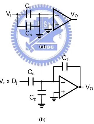
Figure 2.9 (a) MDAC in sample mode (b) MDAC in hold mode... - 16 -
Figure 2.10 Ideal voltage transfer curve in 1bit ADC... - 18 -
Figure 2.11 Voltage transfer curve with offset in 1bit ADC ... - 19 -
Figure 2.12 Ideal voltage transfer curve in 1.5bit ADC... - 20 -
Figure 3.1 The proposed Cyclic ADC architecture... - 22 -
Figure 3.2 (a) The proposed Cyclic ADC scheme ... - 23 -
(b) Timing diagram ... - 23 -
Figure 3.3 The time diagram and operation of each block ... - 24 -
(a) Sample to the input single capacitor and compare ... - 25 -
(b) Hold and subtract to the residue (c) Amplify the residue and compare ... - 25 -
Figure 3.5 (a) Traditional folded-cascode opamp scheme ... - 27 -
(b) Proposed low power opamp scheme ... - 27 -
Figure 3.6 Transition behavior comparison (a) Conventional folded-cascode ... - 30 -
(b) Lower current (c) Adding Me1 and Me2 (d) Complete slew rate enhancement ... - 30 -
Figure 3.7 Comparator scheme ... - 33 -
Figure 3.8 500 times Monte Carlo simulation (a) Vr=25mV (b) Vr=75mV ... - 35 -
(c) Vr=125mV (d) Vr=175mV (e) Vr=225mV (f) Vr=275mV (g) Vr=325mV... - 35 -
Figure 3.9 Calibration circuit ... - 37 -
Figure 3.10 Open-Loop amplifier ... - 37 -
Figure 3.12 FFT of the open-loop amplifier ... - 39 -
Figure 3.13 Error amplifier scheme ... - 40 -
Figure 3.14 Error amplifier transition behavior ... - 41 -
Figure 3.15 Clock generatior scheme ... - 42 -
Figure 3.16 Timing diagram (a) proposed clock pulse waveform ... - 43 -
(b) Simulation result ... - 43 -
ix
Figure 4.2 Simulated FFT ,and at sampling rate=10MS/s ... - 46 -
(a) Pre-simulation and 1MHz input (b) Pre-simulation and 5MHz input... - 46 -
(c) Post-simulation and 1MHz input (d) Post-simulation and 5MHz input... - 46 -
Figure 4.3 Pre-simulation and post-simulation in Corner... - 47 -
(a) Pre-simulation and post-simulation SNDR in corner ... - 47 -
(b) Pre-simulation and post-simulation SFDR in corner ... - 47 -
Figure 4.4 DNL and INL (a) Pre-simulation and post-simulation DNL... - 48 -
(b) Pre-simulation and post-simulation INL ... - 48 -
Figure 4.5 Power consumption of each block... - 50 -
Figure 4.6 The environment of measurement ... - 51 -
Figure 4.7 The die photo of the ADC ... - 52 -
Figure 4.8 The sine wave of the ADC output ... - 52 -
Figure 4.9 The DNL of the ADC ... - 53 -
-- 1 --
C
HAPTER
1
I
NTRODUCTION
1.1
Motivation
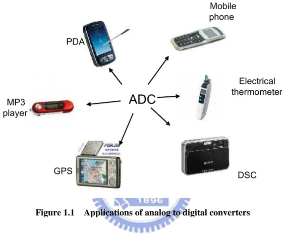
ADC
PDA MP3 player Mobile phone Electrical thermometer DSC GPSFigure 1.1 Applications of analog to digital converters
There are a huge amount of portable devices and consumer electronics products applied in recent years. The characteristics of the products -light, cheap, and lasting- are popular with modern people. Chipsets with more versatility and less power are continually designed.
With the improvement of the techniques for semiconductor fabrication, digital circuits that carry the advantages of faster speed, less power and more noise immunity are adopted in a variety of applications. Utilizing the digital circuits in the profound process will easily bring the characteristics needed. However, unfortunately digital circuits work in the interval while in the natural world, all the physical phenomena exist and transmit in the mode of continuous time. An interface to connect
- 2 -
discrete-time domains and continuous-time ones is required.
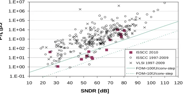
This interface transfers the received analog waveform to digital codes under sampling rate of the system. To be the part of portable device, the chip with analog to digital converter satisfies the low power constraint. Figure 1.2 [1] shows the surveys
of ADC from 1997 to 2010. The figure-of-merit (FOM) is expressed as
2ENOB Power FOM Conversion rate = × (1.1) where ENOB means effective number of bit.
1.E-01 1.E+00 1.E+01 1.E+02 1.E+03 1.E+04 1.E+05 1.E+06 1.E+07 10 20 30 40 50 60 70 80 90 100 110 120 SNDR [dB] P /fs [ p J ] ISSCC 20 10 ISSCC 19 97-200 9 VLSI 1997-2009 FOM=100fJ/conv-step FOM=10fJ/conv-step
Figure 1.2 ADC performance survey from 1997 to 2010
Among many types of CMOS ADC architectures, a cyclic (or algorithmic) architecture achieves efficient power consumption and chip area under middle sampling frequency and resolution which is about 1 to 10MS/s and 8 to 10 bits [2]. Low-power small-area ADCs with 10bit resolution and several tens of MS/s sampling rate are considered to be one of the significant components in battery-operated commercial applications including data communication and image signal-processing systems.
- 3 -
In this research, the power consumption is expected to be as low as possible under 1.8 V power supply in whole circuit. A 9-bit 10MS/s cyclic A/D converter has been designed and implemented with standard TSMC 0.18µm CMOS 1P6M process, and the total power consumption without output buffer is about 3.6mW.
1.2
Thesis Organization
This thesis is organized into five chapters.
In Chapter 1, the motivation and the organization are briefly described. In Chapter 2, the fundamental concepts of analog-to-digital conversion and performance metrics used to characterize ADCs are introduced. Afterwards the cyclic ADC and the similar architecture SAR and pipeline including MDAC (multiplying DAC) and single capacitor scheme are reviewed. The cyclic architecture is described in detail from its basic operations to the actual implementations. The 3.5-bit architecture is utilized to speed up the sampling rate.
Chapter 3 describes the details of each building block. The key circuit blocks used in the low-power ADC is presented. Among them are the proposed low power operational amplifier, the open-loop amplifier for residue amplification, the comparator and the clock generator. Later, transistor level simulated results of each circuit are shown.
Chapter 4 shows the overall simulation results, including the chip layout, the system simulation results, and the measurement considerations. The simulation results for the cyclic ADC fabricated in a standard TSMC 0.18µm CMOS technology are summarized.
- 4 -
- 5 -
C
HAPTER
2
A/D Fundamentals
2.1
Abstract
At first, this chapter describes the overview of analog to digital conversions and discusses some important characteristics to judge the ADCs. Afterwards, it introduces some analog-to-digital converter (ADC) architectures, including flash ADC, Successive-Approximation-Register (SAR) ADC, pipelined ADC and cyclic ADC which are used in the most purposes [3]. The common issues in the design of ADCs will be reviewed. Finally the research focuses on several main building blocks in cyclic analog-to-digital converters.
2.2
ADC Performance Characteristics
The ADC converts the continuous analog signal to discrete digital codes for digital signal processing (DSP) in the next stage. In the start of the conversion, the ADC divides the continuous analog signal into several sub-ranges, and converts to digital codes in the sub-range that the input level is. These steps are continuously processed until all digital codes are resolved. During the process of conversion, the ADC takes the appropriate digital code to the output, and combines the codes by digital circuits. Analog-to-digital converters are characterized by several kinds of indicates to judge the performance, including resolution, SNR, SFDR, SNDR, dynamic range, DNL and INL. On the other hand, the ADC has some non-ideal features, and these features take some imperfections in the performance of ADC.
- 6 -
Resolution means the accuracy of the ADC from continuous analog domain to discrete digital domain, which is also named as effective number of bits (ENOB). The ADC with higher resolution converts more effective digital codes that describe the continuous analog signal more accurately. In other words, the higher resolution of the ADC means the more sub-ranges that input range is divided. In most cases, resolution is defined as the base 2 logarithm of sub-ranges, and is always affected and degraded by noise and nonlinearity in circuits.
2.2.2
Signal to Noise Ratio (SNR)
The signal to noise ratio (SNR) is the ratio of the signal power to noise power and it can be determined by plotting the spectrum in the output of the ADC. The SNR is calculated by measuring the difference between signal peak and the noise floor.
2.2.3
Spurious Free Dynamic Range (SFDR) and Signal to Noise and
Distortion Ratio (SNDR)
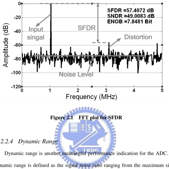
The spurious free dynamic range is the ratio of the input signal level for maximum SNDR to the input signal level for 0dB SNDR. The signal to noise and distortion ratio is the ratio of the signal power to the total noise and harmonic distortion power at the output of the ADC.
- 7 -
Figure 2.1 FFT plot for SFDR
2.2.4
Dynamic Range
Dynamic range is another meaningful performance indication for the ADC. The dynamic range is defined as the signal noise ratio ranging from the maximum signal power input level to the minimum signal power input. It means the range of input signal amplitudes that useful output is obtained from the whole system. When the signal to noise ratio is 0dB, the minimum detectable input signal power is the value of the signal power. Figure 2.2 illustrates a plot of SNR versus input level. If the noise power is independent of the level of the signal, the dynamic range is equal to the signal to noise ratio at full scale, but the noise power increases as the signal level increases in some cases, so the maximum signal noise ratio is degraded by the noise and the harmonic distortion of the ADC device normally.
- 8 -
Figure 2.2 SNR versus input power
2.2.5
Differential Non-Linearity (DNL) and Integral Non-Linearity
(INL)
Both DNL and INL are the linearity index of the ADCs. Differential Non-Linearity (DNL) is defined as the difference between a real quantization step and an ideal quantization step. In other words, DNL is the maximum deviation difference between the two successive conversional values on the input axis, and DNL measures the distance of the input steps from one code to the next code.
-( j) j (LSB)
S
DNL D = ∆
∆ (2.1)
Integral Non-Linearity (INL) is defined as the deviation of each transition voltage of each code from the ideal transition level. INL is referred to as the difference between the actual transfer characteristic and the ideal transfer characteristic that the ADC is designed to approximate.
- 9 - ( j) j (LSB) T INL D = ∆ (2.2) 2 FS N A ∆ = (2.3) DNL and INL are plotted as a function of code, and are expressed in terms of least significant bits (LSB) of the input generally.
Digital
Output
Analog
Input
T
jS
j∆
Figure 2.3 DNL and INL
2.2.6
Non-ideality
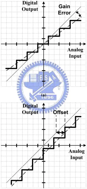
The ideal transfer characteristic of the ADC is obtained from when the successive analog signal from low to high is inputted the ADC, the digital codes corresponding to uniform steps input. In other words, the middle points of every step in input form a straight line, pass through the original point, and then, the most and the last analog input map to the corresponding digital codes. Yet, producing the ideal condition is difficult, because of the gain error, the offset and the non-linearity. The non-linearity is sorted into DNL and INL.
The gain error and the offset are shown on the figure 2.4 (a) and (b) respectively. In figure 2.4 (a), the gain of the transfer curve is insufficient and is un-identical with
- 10 -
the ideal transfer characteristic. And in figure 2.4 (b), the offset shifts a constant amount with the ideal transfer curve. These non-idealities are mainly caused by mismatch of the sampling capacitors, and insufficient gain of the operational amplifier.
Digital
Output
Analog
Input
Gain
Error
(a)Digital
Output
Analog
Input
Offset
(b)- 11 -
2.3
ADC Architecture
2.3.1
Flash ADC
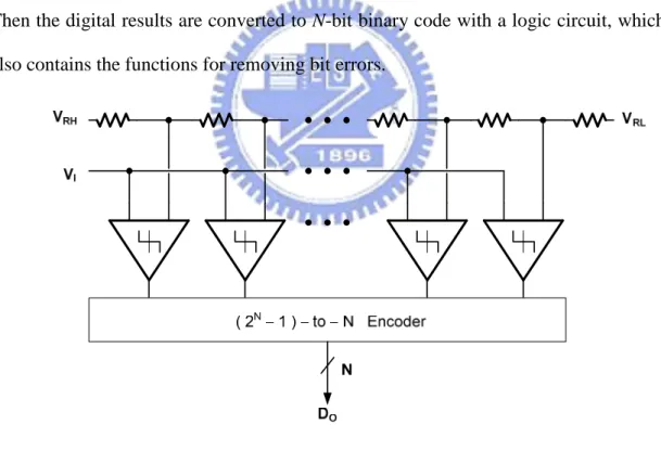
Flash ADC, also called parallel ADC, is the fastest architecture among all the ADCs. In Figure 2.5, the flash scheme includes a large number of comparators to evaluate the analog input immediately. The flash ADC needs 2N−1 comparators to distinguish the analog input from these 2N−1 quantization levels. Every comparator compares the analog input with the reference voltage usually brought by resistor string VRH to VRL. If the analog input exceeds the reference voltage, the output sends
out the “1” in digital domain to the encoder. Otherwise, the output sends out the “0”. Then the digital results are converted to N-bit binary code with a logic circuit, which also contains the functions for removing bit errors.
Figure 2.5 Flash Architecture
The flash ADC can be conducted for a high sampling rate because there is only one comparing cycle used. In other words, the flash ADC needs a large amount of hardware to work simultaneously. On the other hand, increasing the quantity of the
- 12 -
comparators enlarges the whole area of the circuit, as well as the power consumption. Additionally, when used in higher resolution, the tolerable offset of the comparator will be smaller than that used in low resolution. It is a critical point in the circuit design. The high resolution is impracticable for flash ADC, so it can be applied only in the low resolution but with high sampling rate.
2.3.2
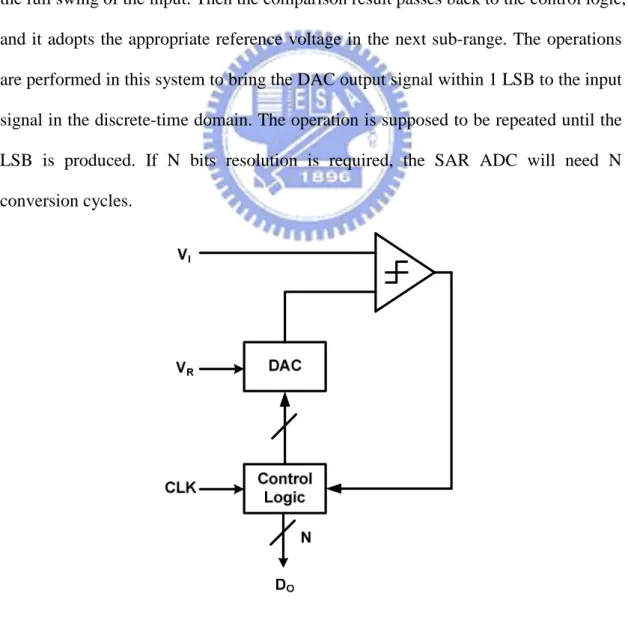
Successive Approximation ADC
The block diagram of Successive Approximation ADC (SAR) is shown in Figure 2.6. At first, analog input signal compares with the MSB, which is the half of the full swing of the input. Then the comparison result passes back to the control logic, and it adopts the appropriate reference voltage in the next sub-range. The operations are performed in this system to bring the DAC output signal within 1 LSB to the input signal in the discrete-time domain. The operation is supposed to be repeated until the LSB is produced. If N bits resolution is required, the SAR ADC will need N conversion cycles.
- 13 -
The operational principle of the traditional SAR ADC is mostly adopted by the charge redistribution, and the MSB is formed by 2N-1 times capacitor respect to the LSB. The resolution can reach up to 14 bits with low power, but the sampling rate is a challenge to produce higher sampling rate. It is an excellent trade-off between accuracy and speed.
In recent years, the newly proposed type of SAR ADC with asynchronous technique can create both the medium resolution and the sampling rate with low power consumption. If the SAR ADC with asynchronous technique meets the demands for the higher resolution and higher sampling rate, it can substitute some ADCs in the future.
2.3.3
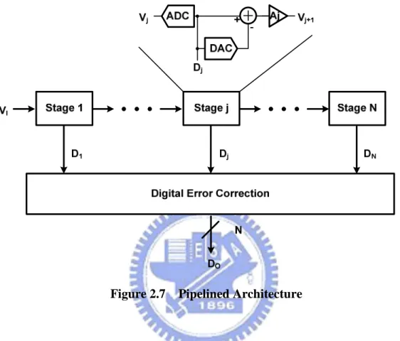
Pipelined ADC
The block diagram of the pipelined ADC is shown in the Figure 2.7. Most of the pipelined ADC adopts the sample-and-hold circuit at the front, and the sample-and-hold circuit takes more accurate data to reduce aperture jitter which happens from the instantaneous value of the analog input. Behind the sample-and-hold circuit, there are the coarse sub-ADC, the coarse sub-DAC, the subtraction, and the amplification of the remainder. In the start of the conversion, the analog input signal compares with the reference voltage, and the sub-ADC resolves digital codes, and drives the sub-DAC to adopt the appropriate reference voltage. In the next clock pulse, the sampling voltage subtracts the reference voltage and the operational amplifier multiplies the residue.
The digital codes are sent to digital error correction logic, and after processing and synchronizing, the digital error correction logic can obtain more accurate N bits digital codes DO. When Vj is processed in stage j, the next analog input Vj+1 is
- 14 -
amplification of the remainder are combined into one single circuit called the multiplying DAC (MDAC).
Figure 2.7 Pipelined Architecture
The Pipelined ADC is applied frequently, because its resolution and sampling rate with less power can bring good F.O.M, and it is suitable for quite a few applications.
2.3.4
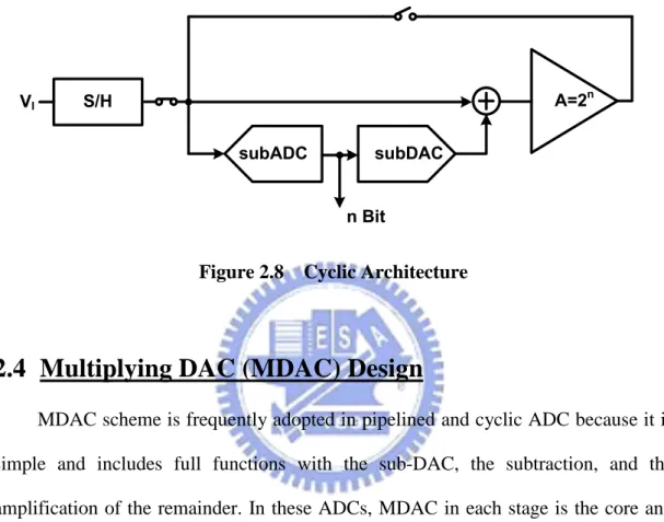
Cyclic ADC
The cyclic ADC just operates the same as one stage in the pipeline ADC shown in the figure 2.8 [4]-[5]. When the conversion is finished in the clock cycle, the output feedbacks the amplified voltage to the front of sub-ADC and the conversion repeats again. Generally speaking, the cyclic ADC can reach the resolution as the pipelined ADC, but the throughput of the cyclic ADC is much less than the pipelined ADC. Even if the sampling rate is less than the pipelined ADC, the cyclic ADC takes
- 15 -
advantages in hardware and power consumption. In deep sub-micro semiconductor process, the more progressive process means more expensive cost. If the cyclic ADC can reach higher sampling rate and keep in the same resolution and power consumption, it will benefit in progressive process by very advantageous active area.
subADC subDAC
A=2n S/H
n Bit VI
Figure 2.8 Cyclic Architecture
2.4
Multiplying DAC (MDAC) Design
MDAC scheme is frequently adopted in pipelined and cyclic ADC because it is simple and includes full functions with the sub-DAC, the subtraction, and the amplification of the remainder. In these ADCs, MDAC in each stage is the core and has two main specifications, accuracy and speed requirements. The accuracy requirement is affected by the feedback factor but mainly dominated by the open-loop gain of the operational amplifier. The speed requirement means the operation speed which is related to the bandwidth of operational amplifier and is also affected by the feedback factor. However, both the requirement of accuracy and speed are depend on the resolution in this stage and remained resolution in the next stage. In other words, the more resolutions in this stage and in the next stage means more difficult to design the operational amplifier.
- 16 -
mode, the VI samples to both capacitors Cs and Cf, and the operational amplifier is in
reset. Then in the next clock phase, hold mode, output of the operational amplifier feedbacks to the capacitor Cf. On the other hand, the appropriate reference voltage
from sub-DAC is switched to the capacitor Cs. According to the charge redistribution,
the transfer function between VO and VI is shown on equation (2.4), which the
parameter ε shown in equation (2.5). And the parameter ε is the error term caused by the finite gain of the operational amplifier and the parasitical capacitor Cp in the input
of the operational amplifier. The feedback factor β in closed-loop of MDAC is shown in equation (2.6). (a)
V
rx D
jC
sC
fV
OC
p (b)Figure 2.9 (a) MDAC in sample mode (b) MDAC in hold mode
(
S)
f j O I r f S 1+ C / C D V = V - V 1+ε 1+ C / C (2.4)- 17 - S f P f C C C 1 = A C ε + + (2.5) f S f P C = C C C β + + (2.6)
If the Cs and Cf are assumed identical to C, then the equation (2.4) could be
simplified to the equation (2.7). When the error term ε is ignored, the equation (2.7) will be the ideal transfer function in a radix 2 stage.
(
)
j O I r D 2 V = V - V 1+ε 2 (2.7)In order to reach N-bit resolution performance, this gain error term should be less than 1LSB of the next stage resolution (z-bit) to prevent the mistakes made by the finite gain of the operational amplifier, as equation (2.8).
2 1 2 P Z C C A + < (2.8) For this reason, the gain requirement of the operational amplifier can be obtained from equation (2.9).
(2 P )2Z
A> +C C (2.9) The equation of the speed requirement for the operational amplifier is derived below. It is assumed that the MDAC in hold mode is a single pole system and ignores the slewing behavior, the MDAC settling time constant is
(
2 P)
u C C τ ω + = (2.10) , and ωu is the unity-gain bandwidth of the operational amplifier in MDAC. Since thesettling error of a single pole system is
2
2
2 ,
T Z
e−φ τ < − Tφ = period in hold mode (2.11) And the constraint of unity-gain bandwidth could be expressed as
- 18 - 2 ln 2 2 P u C Z C Tφ ω > + (2.12)
From the equation (2.9) and (2.12), the gain and unity-gain bandwidth of the operational amplifier in MDAC can be well defined to meet the specification.
2.5
Digital Error Correction
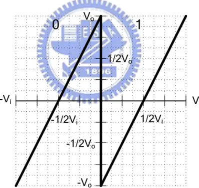
The comparator is commonly used to be the sub-ADC in the most of the ADC. The analog input is compared with the reference voltage by the comparator, and the residue is amplified to the full scale as the input range. The ideal stage gain is 2, and the comparator can be used again in the next cycle. The ideal transfer curve in 1bit ADC is shown in figure 2.10. Obviously, if the input signal Vi is larger than zero, the
comparator will judge the result to logic 1. On the other hand, the comparator will judge the result to logic 0.
-V
oV
oV
i-V
i1/2V
o-1/2V
o1/2V
i-1/2V
i1
0
Figure 2.10 Ideal voltage transfer curve in 1bit ADC
However, the offset of the comparator is a problem to affect the accuracy of the comparison result so that the offset degrades the performance of the ADC. The offset of the comparator is shown in figure 2.11. The offset of the comparator will bring out the wrong comparison result, and the amplified residue can cause the voltage overflow in the next stage. The influence will produce the missing code and transmit to the next stages.
- 19 -
Figure 2.11 Voltage transfer curve with offset in 1bit ADC
The digital error correction [6][7] is utilized to tolerate the offset of the comparator without producing missing code. There are 2 comparators in the digital error correction that the comparators can judge the analog input voltage to three digital codes, “00”, “01”, “10”, and the voltage transfer curve is shown in figure 2.12. In the next stage, the amplified residue is still compared with the same reference voltage. Afterwards, imposing the digital codes from the first stage and the next stage can obtain the accurate 2 bits digital codes.
The tolerant offset of the comparator can reach up to ±1/2 LSB. In other words, if the offset of the comparator is less than ±1/4 Vref, the digital codes after imposing in
digital error correction are still accurate. Because the digital error correction is simple and can tolerate more offset of the comparator without producing missing codes, this technique is extensively utilized.
- 20 -
- 21 -
C
HAPTER
3
CIRCUIT DESIGN
3.1
Cyclic ADC Design
3.1.1
Design Issue
Considering of low power and the efficiency of chip area when operating in middle sampling rate such as ten mega samples per second and middle resolution (about 8 to 10 bits), cyclic ADC is chosen to achieve this target. But it is difficult to keep operating in the sampling rate higher than mega samples per second without increasing much more hardware and power consumption.
To reduce the power consumption of the Cyclic ADC, removing the sample-and-hold circuit in the front-end is one solution. Although removing the sample-and-hold circuit in most of the pipelined ADC architecture will enhance the aperture jitter which is because the voltages caught by comparators and sub-DAC are not identical at the same time. This kind of error will lead to the wrong result and shift codes to the next stages, especially in the neighborhood of the reference voltage in comparators. This issue could be mitigated by operating in slower speed which is not as fast as most pipelined ADC and utilizing the digital error correction technique to tolerate more offsets from comparators and sub-DAC.
Generally, the cyclic ADC is operated lower than ten mega samples per second because there is only one or two stages hardware used which is less than in the pipelined ADC. Otherwise, operating in higher sampling rate means needing more hardware and power consumption, and the operational amplifier in MDAC will be hard to design to satisfy the requirements of both the gain and the bandwidth. In this design, the open-loop amplifier is instead of MDAC scheme to be multiplication circuit in every conversion cycle. This substitute could enlarge the feedback factor in
- 22 -
closed-loop to 1 almost and ease the design requirement in operational amplifier when operating in higher sampling rate, and could reduce the numbers of capacitors array from 16 to 10 in 3.5bits per cycle usage.
On the other hand, to enhance the total conversion rate, this work is adopted to produce multi-bits output per cycle more than 1.5bit per cycle in common usage, and it is 3.5bits here. Besides multi-bits per cycle, the time re-scheduling technique is also applied to speed up so that the total conversion time can be shorten.
3.1.2
Architecture
3.5 bit 3.5 bit 3.5 bit 3.5 bit9-bit digital output Input 9 -Vr 3 Vr 3 Vr 3 3 ADC DAC -+ 8 3 VREF 8VREF Time Reschudualing
Figure 3.1 The proposed Cyclic ADC architecture
Figure 3.1 shows the proposed architecture which including the calibration circuit. There are several methods including open-loop amplifier with the calibration circuit, multi-bits processing and time re-scheduling technique are adopted to improve the higher sampling rate and enhance the efficiency of the chip area. Because this work is used to process 3.5bits every cycle, so the stage gain is 8 which the residue is multiplied into. The calibration circuit is added to ensure the voltage gain of the
- 23 -
open-loop amplifier is 8. After 3.5 conversion cycles, 9 bit digital codes will be produced in the end of the total conversion.
Each block in cyclic ADC will be introduced subsequently. The clock generator provides asynchronous clock pulse which the front of 2 stages are longer, and in the 3rd conversion cycle is half of the first 2 stages, then in the last conversion is half of the 3rd stage again. This time re-scheduling technique is asynchronous and could save more conversion time in the numbers of the next stages.
(a) (Φ1) (Φ2) TS (ΦC) (Φ3) 3.5b + 3.5b + 3.5b + 3.5b = 12 (b)
Figure 3.2 (a) The proposed Cyclic ADC scheme
- 24 -
The proposed Cyclic ADC scheme and the timing diagram are shown in the Figure 3.2. At the phase clock1, analog input signal is compared with the reference voltages in sub-ADC and sampled to the input single capacitors at the same time. Later, at the phase clock2 the appropriate voltage is provided from the comparing result to be subtracted with the sampling voltage by the input single capacitors when the operational amplifier is in negative feedback. The residue voltage after subtracting will be amplified by the open-loop amplifier at clock3. And repeat the operation between amplifying and subtracting. At the phase clockC, the comparators will evaluate the sampling voltage and produce digital codes to digital error correction. On the other hand, at the phase clock2, the operational amplifier subtracts and holds the residue quickly. Figure 3.3 shows the time diagram and operation of each block.
C : Compare H : Hold S : Sample A : Amplify S H S H S H S C C C C A A A S/H enhancement OP amp Comparator 8X amplifier
- 25 -
Figure 3.4 The operations of the proposed Cyclic ADC
(a) Sample to the input single capacitor and compare
(b) Hold and subtract to the residue (c) Amplify the residue and compare
Figure 3.4 shows the detailed operations of the cyclic ADC. In the figure 3.4(a), the analog input signal samples to the capacitor C1, and compares with the reference voltage. The comparators resolve the digital codes and capacitor C2 switch to the appropriate voltage from sub-DAC to storage the residue voltage such as shown in figure 3.4(b). During the next phase clock3, the residue voltage is amplified to full range by the open-loop amplifier which stage gain is 8. At the same time, the amplified voltage is sampled to the capacitor C1 and is compared again which plotted in figure 3.4(c). The operations are repeated from figure 3.4(b) to figure 3.4(c), until the last comparing cycle is finished. Besides, to reduce the power consumption, it is proposed the slew-rate enhancement operational amplifier to save power and maintain the dc gain without sacrificing the behavior in transition.
- 26 -
3.2
Each Block of Cyclic ADC
3.2.1
Slew-Rate Enhancement Operational Amplifier
The operational amplifier is the most critical device in MDAC scheme of the pipelined or cyclic ADC. The dc gain of the operational amplifier dominates the accuracy in each stage, and the unity gain bandwidth dominates the settling speed when in closed-loop. If it is designed to be operated in higher sampling rate, the unity gain bandwidth of the operational amplifier in closed-loop must be much higher. In other words, this means more current in output and more power consumption in whole scheme. On the other hand, more output current causes the lower output resistance and dc gain, and is very disadvantageous to the total resolution. So it needs more and more current and power to maintain the requirements both of the gain and unity gain bandwidth. Therefore, to improve the sampling rate and maintain the same resolution without increasing much power is a difficult problem. Although the proposed cyclic architecture eases the requirement of both dc gain and unity-gain bandwidth of the operational amplifier, but reduce the power consumption with high gain is still urgent for the design.
- 27 -
(b)
Figure 3.5 (a) Traditional folded-cascode opamp scheme
(b) Proposed low power opamp scheme
Figure 3.4(a) shows the traditional folded-cascode operational amplifier which is utilized in high gain and high bandwidth commonly. The dc gain of the traditional folded cascade operational amplifier is
0 M1
A =g ROut (3.1) From equation (3.1), the relation between gM1, Rout and current are shown as
below respectively in ∝ ∝ M1 1 1 1 ,and a Out b g I R I (3.2)
And if Ia1
≒
Ib1, the relation between gain and current would be∝ 0 1 1 A b I (3.3) ∝ b1 SlewRate I (3.4) When the dc gain is designed higher, the current Ib1 should be smaller. On the
- 28 -
larger. It is a trade-off between dc gain and conversion speed here.
The proposed slew-rate enhancement operational amplifier with low power is shown in figure 3.4(b). At first, adding the Me1 and Me2 is a solution. Because when
the operational amplifier is in negative feedback, the operational amplifier is in slewing, and VX or VY drops and turns on one of Me1 and Me2. The turned-on PMOS
provides additional transition current to finish the slewing transition. For example, if Vi- is high and drives the M2 in linear region, VY must be pulled to low voltage. Then
Me2 will be turn on by VY, and provides an immediate current Ic1 to charge Vo- so that
Vo- can follow Vi- and speed up the transition behavior in shorter time.
But this transition behavior is single end to the output, so Me3 to Me8 are added
to make the transition behavior more balanced. The operation of slew rate enhancement will be the same as before. Besides, when VY is pulled to low voltage,
not only Me2 but also Me4 are turn on. Depending on the current mirror formed by Me7
and Me8, it could provide the current Ic2 which is similar to Ic1 to discharge Vo+ so that
Vo+ could follow Vi+ as soon as possible. During the slewing period, the slew rate of
the operational amplifier is shown in equation (3.5) and is larger than the conventional one.
(
)
∝ b1+ c1+ c2
SlewRate I I I (3.5) The transition behavior comparison results between the slew-rate enhancement operational amplifier and the conventional one are shown in figure 3.5. In the figure 3.5 (a), it is the conventional folded-cascode operational amplifier transition behavior in sample and hold mode, and its slew-rate is 132M V/sec. When reducing output current Ib1 to maintain high gain and reduce power consumption, the slew-rate is
115M V/sec which is plotted in figure 3.5 (b) lower than before. In figure 3.5 (c), adding the Me1 and Me2 improves the slew-rate and maintains in high dc gain. The
- 29 -
slew-rate is 149M V/sec, and the additional current Ic1 is about 37.7µA. The complete
transition behavior of the slew rate enhancement operational amplifier with Me1 to
Me8 is shown in figure 3.5 (d). The additional slewing current Ic1 is about 37.7µA and
Ic2 is about 37.4µA, and the slew-rate is 164M V/sec. From the comparison plots, the
slew rate enhancement operational amplifier can reach faster slewing and lower power consumption than the conventional folded-cascode one.
When slewing is finished in negative feedback of the operational amplifier, input pairs M1 and M2 are recovered to saturation region, then VX and VY will turn off
the Me1 to Me4 like switches. The additional MOS switches are turn on in transition
without affecting the gain or unity-gain bandwidth obviously.
(a)
- 30 -
(c)
(d)
Figure 3.6 Transition behavior comparison (a) Conventional folded-cascode
(b) Lower current (c) Adding Me1 and Me2 (d) Complete slew rate enhancement
The relationship between Ia1 and Ib1 is a question. In the conventional
folded-cascode operational amplifier, the currents in the input stage and the output stage are equivalent roughly. Now, decreasing the current Ib1 to enlarge the DC gain,
and keeping the current Ia1 to maintain the total transconductance are feasible. How to
estimate the ratio between Ia1 and Ib1? It can be obtained from the requirement of
stability in the closed-loop. If the requirement of phase margin is designed to 63°, it means the relationship between the dominant pole and the 2nd pole is shown in equation (3.6). nd 1 2 pole 1 2 PM tan ( ) tan ( ) = 63 dominant pole t f f − − = = ° (3.6) The dominant pole and the 2nd pole are defined as in equation (3.7). The parameter gm1 and gm5 are the transconductance of the M1 and M5 respectively in
- 31 -
figure 3.4. CL is the output loading, and Ct is the total capacitance of the node X.
1 5 2 , 2 2 m m t L t g g f f C C π π = = (3.7) The equation (3.6) and equation (3.7) can be combined to the equation (3.8). The ratio between gm1 and gm5 can be found out so that the current Ia1 and Ib1 can also
be designed.
m1 m5
: 2 g :g
L t
C C = (3.8) From the equation (2.6), the feedback factor could be defined as the ratio between thee feedback capacitor and sampling capacitor. And in this proposed architecture, the feedback and sampling capacitor are the same one. Considering the parasitic capacitor in the input of the operational amplifier, the feedback factor almost is 1. So that the equation (2.9) and (2.12) could be modified to
1 2N A> + (3.9)
(
)
2 ln 2 1 u N T f φ β Σ + > (3.10) If considering of N=9 bits, the specification of the operational amplifier can be obtained from equation (3.9) and (3.10). So that the dc gain of the slew rate enhancement operational amplifier should be larger than 60.2dB, and the unity-gain bandwidth should be larger than 107MHz. And the input range of the operational amplifier is ±400mV.From the specification calculated from above, the simulation result of the slew rate operational amplifier is compared with the conventional folded-cascode scheme including corners, DC gain, unity-gain bandwidth, phase margin and power in Table 3.1. The total power saving can be up to 21.6% with other similar specification in TT corner. In table 3.2, it lists the post simulation of the slew-rate enhancement operational amplifier, and the specification is still satisfied the requirements described
- 32 -
above.
Table 3.1 Conventional folded-cascode V.S S/R enhancement opamp Conventional folded cascade S/R enhancement (Pre-Sim) Corner TT FF SS TT FF SS Gain(dB) 61.2 58.6 60.1 67.8 63.6 67.3
fu(MHz) 146 148 139 140 147 130
PM(°) 75 76 74 65 68 63
Power(mw) 0.532 0.417 Power saving is about 21.6% (TT)
Table 3.2 Post-simulation of S/R enhancement opamp S/R enhancement (Post-Sim) Corner TT FF SS DC Gain(dB) 67 62 64 Unity-Gain Frequency fu(MHz) 137 145 127 Phase Margin (°) 64 63 61
3.2.2
Comparator
The scheme [8] in this design is shown in Figure 3.6. Because this cyclic ADC adopts 3.5bits per cycle, the sub-region of the full scale is 15, so that the number of the comparator is up to 14 much more than applied in 1.5bits MDAC generally.
This architecture of comparator has three advantages. The first is that there is no static power consumption. The second is the architecture is simple, and the third is it used only one clock to judge the input data. To avoid additional power consumption for so many comparators is important, and the simple architecture and one clock used can implement the layout simple and well.
- 33 -
difference preamplifier and the regenerative latch. When Vclk is low, comparator
operates in reset mode, and the M5 and M6 are off. At the same time, VO1 and VO2 are
charged to VDD caused by M11 and M12 are in linear region. When Vclk is high, the
comparator operates in evaluate mode, and the input voltage compares with the reference voltage. Later, the regenerative latch can keep the comparison result at the falling edge pulse of the Vclk.
M1 M3 M4 M2 M7 M8 M6 Vi+ Vr+ Vr- V i-VDD M9 M10 M11 M12 V o-Vo2 Vclk M8 M5 Vo+ Vo1 Vclk Vclk
Figure 3.7 Comparator scheme
Considering the effect of mismatch and layout asymmetry, the comparator will produce offset voltage. The comparator offset tolerance is about 25mV in this 3.5bit per stage cyclic ADC. To simulate the effect of mismatches, randomly change the Vth0,
channel width (W), and channel length (L) variations. The standard deviations are as below
- 34 - Vt t A σ(∆V )= WL A σ(W) = W WL β (3.11)
In the 0.18µm TSMC CMOS technology, parameters are shown in table 3.3
Table 3.3 Mismatch parameter
From 500 time Monte Carlo simulations, the distribution of offset voltage is plotted in figure 3.7(a) to (g). Because there are 14 sets of comparator in this architecture for 3.5bits per cycle, it needs to simulate for 7sets different reference voltage. By estimating as Gaussian distribution, the standard variation (σ) is 5mV less than 25mV in constraint.
- 35 -
(c) (d)
(e) (f)
(g)
Figure 3.8 500 times Monte Carlo simulation (a) Vr=25mV (b) Vr=75mV
(c) Vr=125mV (d) Vr=175mV (e) Vr=225mV (f) Vr=275mV (g) Vr=325mV
3.2.3
The Calibration Circuit
- 36 -
reference voltage is taken, the residue will be amplified to full scale and start the next cycle of conversion. Figure 3.8 shows the calibration architecture [9] applied in this 3.5bits per cycle of the cyclic ADC. Because it process 3.5bits per cycle, so the residue needs to be amplified 8 times to the full scale, and the architecture adopts the open-loop amplifier to be amplification circuit.
But how large of the stage amplifies by the open-loop amplifier? The calibration circuit with servo loop is adopted to control the stage gain to be 8. The replica amplifier is the same as the open-loop amplifier completely. When the residue is subtracted and hold in clock phase2, the VREF is sampled into the capacitor Cs at the
same time. Later, the VREF is in the input of the replica open-loop amplifier. Because
of the charge sharing effect by the parasitic capacitor in the input, the amplified voltage would be less than 8 times of VREF at clock phase3. Finally, the 8VREF from dc
will be compared with the amplified VREF in the input of the error amplifier. After
comparing the difference between 8VREF and the amplified VREF, the output voltage
passes through the low-pass filter in the backend and feedbacks to the both open-loop amplifier in signal path and the replica in calibration. By adjusting the control voltage, it can provide a signal to fine tune the resistance in both two open-loop amplifiers so that it can control the stage gain is about 8 by the servo-loop. The detail of the open-loop amplifier and the error amplifier are introduced in the below.
- 37 -
Figure 3.9 Calibration circuit
3.2.4
Open-Loop Amplifier
The proposed open-loop amplifier [10] is shown in Figure 3.9, and it provides the amplification for the residue to full scale. The open-loop amplifier is a simple common-source amplifier. The current source MSP1 and MSP2 are added to enhance the
dc gain. Otherwise, to increase the linearity and reduce the gain error, the RS1 and RS2
are added. The voltage Vctrl from the calibration circuit could adjust the resistance of
MR to derive the amplified residue is as near the value of 8VREF as possible.
- 38 -
The gain of this open-loop amplifier is
≈ + + M1 1 0 M1 1 A 1 1 2 D S MR g R g R R (3.12)
If the product of gM1RS1 is much larger than 1, the gain could be simplified to
the ratio between RD1 and the sum of RS1 and the resistor of MR. Because of the
parasitic capacitor effect in the input of open-loop amplifier, the gain of it must be compensated and larger than the stage gain 8, which is shown
≥ × + 0 A P C stage gain C C (3.13)
, and the trend chart between the DC gain of the open-loop amplifier and Vctrl is
plotted in figure 3.10.
- 39 -
Figure 3.12 FFT of the open-loop amplifier
To ensure the linearity of the open-loop amplifier, it can be verified from the FFT simulation, which is shown in figure 3.11. In the figure 3.11, except the main signal tone in 1MHz, the more obvious signal tone in 3MHz from 3rd harmonic distortion is about -54.4dB. The 3rd harmonic distortion is much less -44dB which is the requirement of remained resolution after 1st amplification.
Besides considering of dc gain, the unity gain bandwidth is the other important specification in the design of the open-loop amplifier. From the step response in equation (3.14), the speed requirement can be simplified to equation (3.15). N is the residual resolution,
τ
a is the time constant of the open-loop amplifier, and ts is the time for residue voltage amplifying. The unity gain bandwidth from equation (3.15) should be larger than 300MHz, and it is 322MHz in this design.τ − = − / (1 t a) o step V V e (3.14)
τ
>0.69( +1) s a t N (3.15)- 40 -
3.2.5
Error Amplifier
The error amplifier is in the calibration circuit and is responsible to verify the comparison result between the amplified residue and 8VREF, and drives the Vctrl after a
low pass filter. It is composed by a dual source couple pair which verifies and amplifies the difference, and a negative transconductance load which enlarges the gain. The amplifier cascades the common source amplifier to transmit out the comparison result from differential to single end. The figure 3.12 shows the scheme of the error amplifier. The dc gain of the error amplifier is 49.4dB, and total power consumption is about 0.64mW. On the other hand, the transition behavior in servo loop is shown in figure 3.13, and the settling time form static to active is less than 800ns.
- 41 -
Settling time
< 800ns
V
ctrlTransition time
Figure 3.14 Error amplifier transition behavior
3.2.6
Clock Generator
Figure 3.14 is the proposed clock generator architecture adopting the time re-scheduling technique. The clock pulse from the clock generator is not the same but asynchronous for decreasing the time in process in the remained cycle because of the remained resolution is not as many as initial condition.
- 42 -
Figure 3.15 Clock generatior scheme
It is composed by frequency dividers, the multiplexer and delay chains. When the clock signal from outside pulse generator inputs the local clock generator, the 3 frequency dividers in series connection divide the 200MHz pulse form outside into 100MHz, 50MHz and 25MHz respectively. The function of the first divider is applied to get pulse with less noise and synchronous for all pulse produced from the clock generator. The D-Flip Flops with set/reset function are series in connection, and ensure the pulse could be a cycle. Then the pulse from the D-Flip Flops circle can pass the delay chains and compose the clock pulse for this cyclic ADC. The proposed waveform is shown as figure 3.15(a), and the simulation result is shown in figure 3.15(b).
- 43 - (a) VΦ1 VΦ2 VΦ3 VΦC (b)
Figure 3.16 Timing diagram (a) proposed clock pulse waveform
- 44 -
C
HAPTER 4
E
XPERIMENT
R
ESULT
4.1
Floor Plan and Layout
The implementation of the cyclic ADC has been integrated in a 0.18µm CMOS process. The active area of the ADC is 0.7×0.3mm2 and the die size is 1.2×0.86mm2. Figure 4.1 shows the layout and floor-planning of the chip. The analog and digital parts are separated and main circuit such as operational amplifier and open-loop amplifier are far away from digital circuit for noise issue. The comparators, switches and capacitors array are placed between digital and main analog circuits. ESD pads are applied in all input and output of the chip.
- 45 - VCKT Vra-Vra+ Vcm_amp VCLK VDD_D VSS_E Vr-Vr+ Vcm_op VDD_E VSS_D Encoder and digital circuit Clock generator OP 8x
Amp Replica R-string
Cal amp Switch Capacitor R-string Com-parator switch Analog Digital Analog Digital (b)
Figure 4.1 The diagram of chip (a) layout (b) floor-planning
4.2
System Simulation Result
4.2.1
Dynamic Simulation
Figure 4.2 shows the pre-simulated and post-simulated FFT plot in TT corner. The SNDR, SFDR, and ENOB at 1MHz and 5MHz input signal and at 10MS/s sampling frequency are shown.
- 46 -
(c) (d)
Figure 4.2 Simulated FFT ,and at sampling rate=10MS/s
(a) Pre-simulation and 1MHz input (b) Pre-simulation and 5MHz input
(c) Post-simulation and 1MHz input (d) Post-simulation and 5MHz input
The SFDR when input is in 1MHz and 5MHz are 57.4dB and 58.9dB in pre-simulation. The ENOB when input is in 1MHz and 5MHz are 7.84bits and 7.81bits in pre-simulation respectively. The SFDR when input is in 1MHz and 5MHz are 54.6dB and 56.5dB in post-simulation. The ENOB when input is in 1MHz and 5MHz are 7.79bits and 7.70bits in post-simulation respectively.
- 47 -
(b)
Figure 4.3 Pre-simulation and post-simulation in Corner
(a) Pre-simulation and post-simulation SNDR in corner
(b) Pre-simulation and post-simulation SFDR in corner
The variation from the wafer foundry will affect the characteristics of transistors, so corner simulations for TT, FF and SS are also needed. Figure 4.3 is the SFDR and SNDR plot which is pre-simulation and post-simulation result when input frequency is from 1MHz to 5MHz, and the resolution are above 7.3bits in all corner, especially in FF corner, it can achieve 8 bits. But in SS corner, it will be worse. When sampling in 5MHz, the simulation results will be worse than in 1MHz in all corners generally.
4.2.2
INL and DNL
INL and DNL show the non-linearity performance of this cyclic ADC. Figure 4.4 (a) is the DNL and INL plot in pre-simulation. The DNL is about 0.6LSB, and the INL is about 0.68LSB. In figure 4.4(b), the DNL and INL plot in post-simulation is shown. The DNL is about 0.69LSB and the INL is 0.90 LSB. The linearity is worse in the full swing near ±400mV is because the linearity of open-loop amplifier is not as good as in small swing. The LSB is 9bit resolution to full scale input.
- 48 -
Pre-Sim Post-Sim
(a)
Pre-Sim Post-Sim
(b)
Figure 4.4 DNL and INL (a) Pre-simulation and post-simulation DNL
(b) Pre-simulation and post-simulation INL
4.2.3
Specification Table
Table 4.1 shows the performance summary simulated in 0.18µm TSMC CMOS process. The conversion rate is 10MS/s and the resolution is 9bit. In post-simulation, the ENOB is 7.84bit and 7.81bit at input frequency is 1MHz and 5MHz, respectively. The total power is 3.6mW. Then the digital circuit consumes about 1.5mW, and
- 49 -
analog circuit consumes 2.1mW. The detailed power distribution is shown below in figure 4.5.
The FOM is defined as
2ENOB Power FOM Conversion rate = × (5.1)
In this design, the FOM is 1.7pJ/Setp at input frequency is 1MHz and at post-simulation.
Table 4.1 ADC specification of pre-simulation and post-simulation
Pre-sim
Post-sim
Technology
0.18µm CMOS process
Resolution
9bit
Supply voltage
1.8V
Signal Swing
+/-400mV
Conversion rate
10MHz
SNDR
48.77dB @ 1MHz input
49.02dB @ 5MHz input
48.66dB @ 1MHz input
47.12dB @ 5MHz input
ENOB
7.81bit @ 1MHz input
7.85bit @ 5MHz input
7.79bit @ 1MHz input
7.70bit @ 5MHz input
2.1mW [Analog]
1.5mW [Digital]
Power consumption
3.6mW [Total]
- 50 -
Figure 4.5 Power consumption of each block
4.3
Experiment Result
4.3.1
Measurement Consideration
The environment of measurement is shown in figure 4.6. The analog input signal is generated from the signal generator E4438C manufactured by Agilent. Then the analog input signal passes through the band-pass-filter (BPF) which filtered out the noise. At the back of the band-pass-filter, the balun is applied to transform the single end signal to differential end, then the differential signal transmits into the chip on the PCB. All the analog and digital power supplies and dc bias current are supplied from Agilent E3630A power supply, and the clock pulse is generated from the pulse generator Agilent 8133A. After the conversion is finished, the resolved digital codes are sent to the logic analyzer Agilent 16700. At last the data could be downloaded to the personal computer, and is processed to calculate the SNDR, SFDR and INL and son on… by Matlab.
- 51 -
Figure 4.6 The environment of measurement
4.3.2
Measurement Result
The die photo of this ADC is shown in the figure 4.7. The relative sine wave of the ADC digital output when the analog sine signal inputs is shown in the figure 4.8, and it is expressed by decimals. The figure is similar to the triangular wave caused by the 4th pad output inactive, and there is no any obvious voltage variation near ground from this pad when the analog input varies. Therefore the 4th pad can’t bring out logic 1 to contribute to this conversion. Besides, the lost digital code might cause the output failed to calculate the total conversion performance of 9 bits from FFT. The DNL is about +43 / -1 LSB and the INL is about +38 / -39 LSB which are plot in the figure 4.9 and figure 4.10 respectively. Even though the total performance can’t be shown from FFT plots easily, some things still could justify the chip is active. At first, the digital output could follow the varying analog input like the figure 4.8 which means the total operation is normal in the analog circuit. Otherwise the residue could be wrong or the output of the open-loop amplifier could be saturated and the digital output of the ADC must not be able to like shown. And second, the abnormal DNL
- 52 -
and INL plots are caused from the lost digital code in 9bits resolution. But if the linearity range backed to the first 3 bits, the INL range could be regarded as less than 1 LSB. It means the 1st conversion cycle is active. Both above the two reasons, the ADC could be active if the 4th pad is normal.
Figure 4.7 The die photo of the ADC
- 53 -
Figure 4.9 The DNL of the ADC
- 54 -
C
HAPTER 5
C
ONCLUSION
Table 5.1 summarizes the benchmark of the performance for the cyclic ADC. The power supply is 1.8V in this work, and the SNDR is 48.68dB and ENOB is 7.79bit in simulation at sampling rate is 10MS/s and input frequency is 1MHz. The FOM shows 1.7pJ/step. Compare to other references shown in table I, the FOM performance is better than [11]-[14] especially in power consumption. Otherwise, the paper [15] is better in power consumption, but the sampling rate is only 1MHz less than this thesis. Although the improvements of these ADCs [15]-[17] are obvious in FOM, the similar techniques and concepts are adopted such as timing re-schedule and multi-bits throughput.
Table 5.1 Performance summary of cyclic ADC
2005 JSSC[11] 2009 JSEN[13] 2006 VLSI[12] This Work Technology 0.18µm 0.18µm 0.13µm 0.18µm
Type Cyclic Cyclic Cyclic Cyclic
Supply Voltage 0.9V 3.3V 3V 1.8V
Resolution 12bit 10bit 11bit 9bit
Conversion Rate 5MS/s 14MS/s 10MS/s 10MS/s SNDR 50dB 52.44dB 56dB 48.68dB Power 12mW 21.62mW 15mW (ADC 10.5mW DLL 4.5mW) 3.6mW DNL/INL 0.6/1.4 0.79/1.89 0.9/3.5 0.69/0.9 Active Area 1.4mm2 0.381mm2 0.19mm2 0.21mm2 FOM(pJ/step) 9.3 4.5 2.9 1.7 2ENOB Power FOM Conversion rate = ×