埋置式閘極功率高電子遷移率電晶體
74
0
0
全文
(2)
(3) 致謝 首先感謝指導教授陳宏任博士在作者碩士班就讀期間所給予課業上的指導以 及資源上的提供,並在課外之餘,願意分享之前在業界的心得與看法給作者,讓 作者感到受益良多,實在是一位令人尊敬的良師兼益友。. 接著感謝海洋大學羅文雄博士在實驗以及論文上的指導,讓作者明瞭要成為一 位學術達人是需要多麼專注在學問研究上,還有譚仕煒學長、已畢業的天聲學長 和黃光實驗室的威鈿學長、孟凱學長、和紹諺學長在學術與做人處事方面的指 導,冠旭、穎潔同學在實驗和生活上的互相協助。 還有成功大學劉文超博士在 口試及論文上對作者的指教,希望往後還有機會接受劉博士的指導。. 另外也要感謝高雄大學施明昌博士在提供製程實驗的學習機會,還有班代鴻儒 及光電組豈瑋、世昌、順昌同學在碩士班期間彼此互相扶持,不論是學校課業的 指導還是校園資訊的提供都是功不可沒。特別是豈瑋,在作者北上實驗,不畏學 校惡勢力持續全力支援並協助作者,確實是位値得信賴的夥伴。 還有系上親切 可愛的系辦助理姿蓉,有你的協助我才能在計畫申報處理更加順利。 還有二中 同學品佑,在我初次來到人生地不熟的基隆,提供住宿及交通接送。. 最後要感謝家人願意給作者在學問精進上的一次機會,並感謝多年來對作者的 栽培及養育之恩,還有老弟在生活瑣事上的協助,此外也要感謝女友芷寧的支 持,四年來與作者相互扶持,讓作者的碩士生涯有所精神寄托。 並謝謝所有認 識我和愛我的朋友,我愛你們大家,. 真的要謝的人太多了,那就謝天吧。.
(4) 埋置式閘極高性能高電子遷移率電晶體. 指導教授:陳宏任 博士 國立高雄大學電機工程研究所 學生:蘇志成 國立高雄大學電機工程研究所. 摘要. 本論文研製之 空乏模式砷化鋁鎵/砷化銦鎵雙異質接面高電子遷移率電晶體藉著退 火製程成功出埋置式閘極,埋置式閘極可控制閘極與通道間的距離而用來改善串聯電 阻,使用雙異質接面高電子遷移率電晶體可得到量測值轉移電導 150mS/mm 以及開路電 壓增益 136,而使用埋置式閘極雙異質接面高電子遷移率電晶體(退火溫度 330。C)則可 增進到轉移電導值 175mS/mm 以及開路電壓增益 160。. 良好的元件線性度可藉由汲極電流及轉導關係使用多項式表現法較低的二階對一階 比獲得,藉由三組實驗樣本元件 A(未使用埋置閘極)、元件 B(使用埋置閘極,退火溫度 。 。 280 C)、元件 C(使用埋置閘極,退火溫度 330 C)可得到最大截止頻(最大功率截止頻. 率) 依序為 13.5、13.5 及 14.(35、37 及 37.5) GHz,除此之外,在 2.4 GHz,偏壓在 汲極電壓 3 V 閘極電壓-1.0 V 環境下,元件 C(使用埋置閘極,退火溫度 330。C)展現出 最佳的功率轉換效率 44.8 % 以及最小的雜訊指數 1.46 dB。.
(5) 透過 2-D 模擬軟體,增加埋置式閘極沉入蕭特基層深度因而提高深寬比(沉入閘極 與通道的距離),觀察其能帶及電荷密度變化,比較實驗值與模擬值是否有相同的趨勢 進而提出相同的結論 : 不論是直流或是高頻特性,埋置式閘極均提升元件的性能。. 關鍵字 : 高電子遷移率電晶體、假晶、異質接面、雙異質接面、埋置式閘極、.
(6) Power High Electron Mobility Transistor With a Buried Gate Advisor: Dr. Hon-Rung Chen Department of Electrical Engineering National University of Kaohsiung Student: Chih-Cheng Su Department of Electrical Engineering National University of Kaohsiung. ABSTRACT Depletion-mode Al0.24Ga0.76As/In0.22Ga0.78As double heterojunction high electron mobility transistors (DH-HEMTs) were successfully fabricated with an as deposited gate to compare with those with a buried gate by annealing. Instead of a recessed gate, a buried gate used to control the distance between the gate and channel (and hence the aspect ratio) improves the series resistance. The measured transconductance of 150 mS/mm and an open-drain voltage gain of 136 for the DH-HEMT with an as deposited gate are enhanced to 175 mS/mm and 160 for the DH-HEMT with a 330-℃ annealing gate. Good device linearity is also obtained with very low second-harmonic to fundamental ratio of 3.55 %. The measured maximum fts (fmaxs) are 13.5, 13.5 and 14.5 (35, 37, and 37.5) GHz for DH-HEMTs with an as deposited, a 280-℃ and a 330-℃ annealing gates, respectively. Besides, the DH-HEMT with a 330-℃ annealing gate exhibits the highest PAE=44.8% and the lowest Fmin=1,46 dB at 2.4 GHz of all d e v i c e s u n d e r t h e b i a s c o n d i t i o n o f t h e V D S = 3 V a n d V G S = − 1.0 V.. Sinking gate metal into the Al0.24Ga0.76As Schottky barrier and hence changing the aspect ratio (Lg/deff, defined by the ratio of the gate length over the distance between the gate and.
(7) channel) were employed in the simulation. The theoretical analysis and simulation are made by using a two-dimensional simulator Atlas. Based on the variations of the gate-metal sinking depth, the dc and rf performances are compared and studied. Keywords: pHEMT, HEMT, pseudomorphic, DH-HEMTs, heterojunction, doubleheterojunction, buried gate,.
(8) 第一章 導論. 隨著科技的日新月異,無線通訊已進入高頻傳輸的時代,在毫米波功率應用方面, 需要一種具有高頻特性以及高電流驅動能力的主動元件,高電子遷移率電晶體(HEMT) 是其中一種具備高頻特性的理想元件。 單異質接面結構的高電子遷移率電晶體利用電 子提供層來展現高電流增益、高頻性能及低雜訊指數,然而,限於通道無法摻雜而擁有 足夠的載子數以致造成低電流密度,在載子提供層使用高摻雜則可解決這問題,然而他 也帶來了低崩潰電壓使得功率承載能力受到限制這缺點,另一方面在直流特性裡,它也 發生了"扭結效應" 。 雙異質接面的高電子遷移率電晶體具有兩層載子提供層,其中 一層在通道上方,蕭特基層下方,利用輕摻雜可提供閘極高崩潰電壓並且減少扭結效應 發生而降低輸出電導。 另一層載子提供層則是在通道下大能障層重摻雜來提供足夠的 載子數,同時能障層也可防止電子入射緩衝層。. 接下的章節依續會說明為何採用三五族化合物半導體元件和各個磊晶層的作用,之 後再講解製程步驟及其原理,針對實驗結果作出特性討論與理論分析。.
(9) 第二章 元件結構與製程. 三五族化合物半導體由與具備許多以下優點,固可以應用在光電以及微波領域中: (1) 在低電場(高電場)下,電子在砷化鎵中的移動率為在矽中的 3~5(約 1.5)倍,在砷化銦 鎵中的移動率為為矽的 5~7(2)倍。(2)大部分化合物半導體能隙均大於矽半導體 (1.12eV),故可應用在微帶線及單晶石為波積體電路上做絕緣基板,同時亦可以提高元 件崩潰電壓特性。(3)化合物半導體又稱直接半導體,這是由於電子在價電帶傳輸到導 電帶不需要做動量轉換,直接半導體在發光元件如發光二極體、雷射二極體扮演很重要 的腳色。(4)具有抗幅射特性。(5)化合物半導體可磊晶出良好的異質接面如:砷化鋁鎵/ 砷化鎵或是砷化鋁銦/砷化銦鎵使得載子可侷限在二維電子海提高傳輸速率。. 金半場效電晶體於 1966 年被提出來,主要是由兩個歐姆接觸的汲極和源極及一個蕭 特基閘極所組成,幾乎所有金半場效電晶體都是由化合物半導體所形成,故在傳輸速度 或高頻特型均上比矽-場效電晶體優秀許多,然而通道摻雜所形成的雜質散射限制了元 件高頻的特性。. 從 1978 年開始高電子遷移率電晶體已被成功製造,其原理是讓載子. 傳輸在利用異質接面所形成的二維電子海,而高電子遷移率電晶體又分別發展出不同的 型態。 一般而言,在通道上方會提供一層平面摻雜來提升載子濃度,但是也因此引發 一些不良效應如扭結效應及降低閘極崩潰電壓等,而利用雙異質接面並在下方提供載子 層可解決以上缺點。. 本文研究空乏模式-假晶-砷化鋁鎵/砷化銦鎵雙異質接面高電電子遷移率電晶體是由 分子束磊晶所製造,其結構分別為 0.5μm 砷化鎵緩衝層、超晶格次緩衝層、3.5-nm 掺 雜-能障層、5-nm 砷化鋁鎵空間層、12.5-nm 未摻雜通道層、4.5-nm 砷化鋁鎵空間層、 砷化鎵平面摻雜(δ(n+)=4x1012cm-2)、30-nm 未摻雜蕭特基能障層及 35-nm 砷化鎵覆蓋 層。 其製程包含以下: 元件分離、在汲極源極鍍上金鍺鎳合金、使使用退火技術使成.
(10) 歐姆接觸,在移去覆蓋層後,在蕭特基層上利用高功函數的金屬增加能障以增高崩潰電 壓及降低扭結效應,因此使用金/鉑形成閘極,最後再分別做元件不同退火條件(A:無退 火處理 B:280。C 在氮氣環境 5 分鐘 C:330。C 環境同 B)來形成埋置式閘極,控制其沉入 深度,然後做直流及高頻特性分析。.
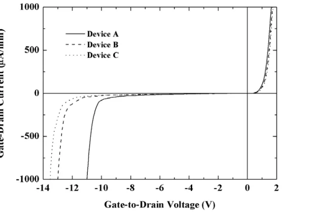
(11) 第三章 實驗結果與討論 圖 3-1 發現閘極-汲極順向開啟電壓依序 1.64(A)、1.72(B)及 1.76(C)伏特,在反偏 電壓為-10 伏特量測漏電流為 81(A)、25(B)及 21(C)微安培,並顯示出元件 B、C 在崩 潰電壓特性(13、13.5 伏特)優於元件 A(11 伏特)。. 利用埋置式閘極技術可讓通道區. 的電荷密度不受改變,固發現其通道電阻幾乎相同。 雖然我們利用雙異質接面摻雜來 改善扭結效應,但在 Vgs≥0V 和 VDS≥3V 下,圖 3-2 發現元件 A、B 的汲極電流有下降現 象,一般被認為是由於平行導通效應所造成。圖 3-3 顯示出兩個轉導峰值可應證其推 論,藉由參數萃取可發現元件 C 具有較有優秀的線性度。 圖 3-4 是輸出電導及開路電 壓增益對汲極電壓關係,由圖可發現元件 A、B、C 均有極低的輸出電導且沒發現扭結效 應,使用埋置閘極所產生良好的深寬比使得元件 B、C 的開路電壓增益(170、160)高於 元件 A(136)。. 圖 3-5 指出其元件的高頻性能,由於截止頻率與轉導、總閘極電容相關,隨著下沉 金屬與通道距離的縮短,轉導與總閘極電容則隨之增加,得到最大電流截止頻率(最大 功率截止頻率)依序為 13.5(35)、13.5(37)及 14.5(37.5) G 赫茲。. 圖 3-6 描述了元. 件的功率特性,並發現元件 C 展現最佳的功率轉換(PAE=44.8%)。 圖 3-7 指出元件的雜訊指數與電路增益表現,元件 C 再一頻率在雜訊指數的表現均優於 元件 A,其結果有可能是偏壓電流的差異(190(A)、130(B)及 70(C) mA/mm) 造成,另一 種可能就是元件 C 具有較低的反偏閘極漏電流。.
(12) 第四章 理論分析與模擬 在本章將利用半導體 2-D 模擬軟體 ATLAS 分析利用埋置式閘極沉入蕭特基層深度參數 (h=0, 50, and 75 Å)的不同分析對元件能帶及電荷密度所造成的影響。 圖 4-2(a)~(c)我們觀察到蕭特基層厚度的變化,通道上方的平面摻雜層在正 Vgs 時, 電子可在通道與平面摻雜層有良好傳輸特性,改善平行導通效應進而增加元件線姓度, 而通道下方的掺雜-能障層導電帶不連限續面(△EC),在負 Vgs 時還可防止電子入射緩 衝層。 圖 4-3 為元件在不同 Vgs 偏壓下(VGS=+1 V, +0.5 V, 0 V, and −1 V)的電荷密 度分布圖,通道在 h = 0 Å,Vgs = 0 V 下擁有最大的電荷密度,而電荷密度在 h = 75 Å,Vgs = -1 V 則讓電荷密度驟降,郎好的電荷控制使得臨界電壓隨 h 增加而往正值位 移,在 Vgs 逐漸正偏壓下,電荷開始在通道往 δ 砷化鎵摻雜層流竄,使得電荷控制能 力下降。. 圖 4-4 為汲極電流-電壓三端圖,我們發現懡擬結果元件均展現不錯的夾止特性,不 同於使用閘極蝕刻製程,使用埋置閘極製程的三端塗的歐姆區阻值相當接近,故可以介 此在維持阻值不變的情況下用來改變臨界電壓。圖 4-5 左上發現其沉入深度對應臨界電 壓相當線性,轉移電導(h=0、50、75 Å)依序為 171,186 及 197 mS/mm,說明了沉入 金屬越接近通道,轉移電導就越大,並注意到在 Vgs 接近 0 的地方有一個小峰值,這是 由於通道電荷穿邃至砷化鎵摻雜層效應所造成的結果。利用多項式二階對一階比其線性 度發現元件在 h= 75 Å 非線性度最低(a2/a1 = 0.92 %)而證明了其優異的轉移電導線性 度。. 圖 4-6 再次指出優異的深寬比提供絕佳的電荷控制與電壓增意益(元件 h=0、50 、75 Å 其輸出電導(開路增益)為 6.5 (26), 5.0 (37), and 4.1 (45) mS/mm)。 根據式子 6 隨著沉入深度的增加,轉移電導增加但由於閘極電容也跟著增加,故最大.
(13) 截止頻率改變不大。但是根據式子 7 發現根號內的輸出電導越小會讓最大功率增益頻率 大大提升,圖 4-7 應證上述的說明。.
(14) 第五章 結論. 本論文雙異質接面高電子遷移率電晶體通道上方含有平面摻雜與通道下方使用摻雜能障層結購,在製程上採用金/鉑閘極並在元件完成後利用退火技術形成埋置式閘極。 我們發現其通道下方的摻雜-能障層可減少扭結現象產生,而使用埋置閘極來提升深寬 比可得到更高及較佳線性度的轉導、較低的漏電流及較大的電壓增益,交流特性亦有較 佳的性能,實驗與模擬結果都清楚證明使用埋置式閘極比起閘極蝕刻所製成的元件擁有 較優良的性能。. 在未來的研究,我們可以朝利用埋置式閘極可以控制臨界電壓的原理,使元件型成增 強型元件,並利用元件設計成高速的邏輯電路應用在無線高頻或是光電領域上。 此外, 在高溫環境下,元件的可靠性分析也是將來研究的重要課題。.
(15) Content Abstract (Chinese) Abstract (English) Table Captions…………………………………………………………..I Figure Captions….……………………………………………………...II. Chapter 1 Introduction………………………………………..1 1-1. Thesis Motivation…………………………………………1. 1-2. Thesis Organization……………………………………….2. Chapter 2. Device Structure and Fabrication……………...…..4. 2-1. III-V Field Effect Transistors……………………………..4. 2-2. Traditional HEMT Structure……………………………...8. 2-2-1. Cap Layer…………………………………...…………………….8. 2-2-2. Schottky Layer…………………………………………………….8. 2-2-3. δ-Doping…………………………………………………………..9. 2-2-4. Space Layer……………………………………………………….9. 2-2-5. Channel Layer……………………………………………………10. 2-2-6. Buffer Layer……………………………………………………...10. 2-3. Process Technology……………………………………11. 2-3-1. Mesa Isolation……………………………………………………11. 2-3-2. MS Contact……………………………………………………....12. 2-3-3. Gate Fabrication………………………………………………….15.
(16) 2-3-4. Air Bridge………………………………………………………..17. 2-4. Device Fabrication……………………………………18. Chapter 3 Experimental Results and Discussion……...…26 3-1. DC Characteristics……………………………………26. 3-1-1. GD Diode Characteristics………………………………………..26. 3-1-2. Three Terminal I-V Characteristics…………………………...…27. 3-1-3. Transconductance-Current Characteristics………………………29. 3-1-4. Output Conductance Characteristics……………………………..33. 3-2. RF Characteristics…………………………………….34. 3-2-1. High Frequency Performance……………………………………34. 3-2-2. Power Characteristics…………………………………………....35. 3-2-3. Noise Figure……………………………………………………..36. Chapter 4 Theoretical Analysis and Simulation…………37 4-1. Theory and Simulation……………………………….37. 4-2. Simulation Results and Analysis……………………..39. 4-2-1. Band Diagrams of DH-HEMTs with Different Depth of Schottky barrier…………………………………………………………...39. 4-2-2. Electron Sheet Density…………………………………………..41. 4-2-3. Calculated Current-Voltage Characteristics……………………...43. 4-2-4. Transconductance Characteristics………………………………..44. 4-2-5. Output Conductance and Voltage Gain Characteristics………….46. Chapter 5 Conclusion………………………………..48.
(17) Table Captions. Table 2-1 Work functions of some widely used metals…………..………………….17 Table 3-1 Comparisons of the device linearity between device A, device B, and device C………………………………………………………………………………31 Table 4-1 Device structure of the DH- pHEMT studied in the theoretical analysis………………………………………………………………….37 Table 4-2 Second-harmonic to fundamental ratio (a2/a1) of the devices with a sinking gate-metal depth h = 0, 25, 50, and 75Å………………………………....45 Table 5-1 The experimental results with a buried gate (different depth)…………..48.
(18) Figure Captions Figure 2-1 Schematic cross section of the MESFET………….……….……………...5 Figure 2-2(a) Schematic cross section of. SH-HEMT………………………………5. Figure 2-2(b) Schematic cross section of the of DH-HEMT……………...………….5 Figure 2-3 Bandgap versus lattice constant plots……………………………………..7 Figure 2-4(a) I-V curve of. the Schottky contact………..…………………………13. Figure 2-4(b) I-V curve of the ohmic contact………………………………..…...…13 Figure 2-5(a) Mechanism of TE motion………………………………………..…....14 Figure 2-5(b) Mechanism of FE motion……………………………………….…....14 Figure 2-5(c) Mechanism of TFE motion………………………………..…………..14 Figure 2-6 Cross section of undercut…………………………………….…………..15 Figure 2-7(a) Before gate recess……………………………………………….……16 Figure 2-7(b) After gate recess…………………………………………….……..….16 Figure 2-7(c) After evaporating metal…………………………………………...…..16 Figure 2-8 Air-bridge plot…………………………………………………..…….….17 Figure 2-9(a) Cross section of air-bridge………………………………………..…..18 Figure 2-9(b) Plan view of air-bridge…………………………………………..……18 Figure 2-10 Band diagram of DH-pHEMT……………………………………….....19.
(19) Figure2-11 Schematic cross section of the pHEMT…………………………………20 Figure 2-12 Process procedure of pseudomorphic HEMT……………………….….21 Figure 2-13(a) First the sample was dipped in the alcohol and acetone in the ultrasonic vibrator…………………………………………..…………………..22 Figure 2-13(b) Standard photolithography was used to meas-type windows , and samples were etched by etching solution of H3PO4:H2O2:H2O = 6:3:100 ………………………………………………………………………………………..22 Figure 2-13(c) Mesa isolation was completed……………………………………….22 Figure 2-13(d) Same technology was used to define drain-source type windows.............................................................................................22 Figure 2-13(e) AuGe/Ni were evaporated upon drain-source electrode…………….23 Figure 2-13(f) Sample was dipped in the acetone for lift-off tech………..…...…….23 Figure 2-13(g) To get drain-source metal ohmic contact , we putted the sample on the hot-plate in the temperature for 300。C for 30 seconds….……...…23 Figure 2-13(h) Wet etching tech was used for high selectivity solution by citric acid and gate recess tech was used to dismiss the capping layer between Drain and Source and to gate metallization…………………………………….......….23 Figure 2-13(i) 1-µm gate meal is evaporated on the 3-µm Schottky layer to get the drain current control………………………………………..……………..24 Figure 2-13(j) Using Au/Pt for gate metallization…………………………………..24 Figure 2-13(k) Device process was completed…………………….………………..24 Figure 2-13(l) By annealing process , Au/Pt gate was sinking into Schottky Layer...24 Figure 2-14 Cross-sectional view of DH-pHEMT with a buried gate…………..…..25.
(20) Figure 3-1 Gate-drain current-voltage characteristics of fabricated devices A, B, and C…………………………….…………………………………………...26 Figure 3-2 Measured common-source current-voltage characteristics of fabricated devices A, B, and C…………………………………………………….………..…28 Figure 3-3 Corresponding transfer characteristics (gm and ID vs. VGS) of fabricated devices A, B, and C………………………………………………………….……..32 Figure 3-4 Transconductance (gm), output conductance (gd) and open-drain voltage gain (Av= gm /gd) as a function VDS for all fabricated devices A, B, and C at VGS= -1.0 V………………………………………………………………………..33 Figure 3-5 Experimental microwave performances for devices A to C at VDS = 3 V………………………………………………………………………...34 Figure 3-6 Power performance of all devices A to C with a gate width of 100 µm at 2.4 GHz under VDS of 3.0 V and VGS of −1.0 V……………………………..…...35 Figure 3-7 Relation of the noise figure and associated gain on the frequency………36 . Figure 4-1 The DH-HEMT with a sinking gate depth of h…………………..……...38 Figure 4-2 (a) Band diagrams of DH-HEMT with a 300Å Schottky barrier……......39 Figure 4-2 (b) Band diagrams of DH-HEMT with a 250Å Schottky barrier………..40 Figure 4-2 (c) Band diagrams of DH-HEMT with a 225Å Schottky barrier………..40 Figure 4-3. Electron sheet density of the device with h=0, 50, 75 Å biased at VGS=+1 V, +0.5 V, 0 V, and −1 V……………………………………………..….41. Figure 4-4 Current-voltage (I-V) characteristics of the devices studied: DH-HEMTs with a gate-metal sinking depth of 0, 50, and 75 Å…………………….43 Figure 4-5 Transfer characteristics as a function of VGS………..…….……...….…..44.
(21) Figure 4-6 Output conductance (gd) and open-drain voltage gain (Av) as a function of VDS...........................................................................................................46 Figure 4-7 ft and fmax as a function of VGS………………………………………….47.
(22) Chapter 1 Introduction 1-1 Thesis Motivation. Millimeter-wave power applications demand active devices with high cut-off frequencies and large current driving capability. High Electron mobility transistors (HEMTs) are thought to be one of the most promising devices for high frequency operation due to their good frequency performance [1-6]. Single heterojunction HEMTs (SH-HEMTs) employing one electron supply layer have shown excellent unity current gain frequencies and very low noise figures [1-3]. However, they generally exhibit low current densities due to the relatively small number of electron carriers in the channel. The electron carriers can be enhanced by increasing the doping concentration in the electron supply layer. However, this approach may bring about a reduced breakdown voltage, thus also limiting the final power handle capability [4]. On the other hand, SH-HEMTs have usually been reported to exhibit significant “kink behaviors” in the current-voltage characteristics [7-9]. One of possible origins for the kink is believed to be caused by trapping and detrapping of electrons injected in the buffer at low VDS and then injected back to the channel at high VDS [8, 9]. Double heterojunction HEMTs (DH-HEMTs), where two electron supply layers are employed on each side of the channel, provide the possibility of a large current density. In this way, the upper electron supply layer where the Schottky metal is deposited is not necessary to be highly doped. Thus high breakdown voltage is expected and also a low output conductance thanks to the additional bottom heterojunction [10, 29-30]. This additional bottom heterojunction in the DH-HEMTs can be served as a barrier to 1.
(23) prevent the electrons from being injected into the buffer. Kink-free current-voltage characteristics are also expected.. 1-2 Thesis Organization. In the later chapter2 we firstly introduce MESFET, SH-HEMT and DH-HEMT, respectively. And select DH-HEMT to be the investigating subject in this thesis, later explain the DH-HEMT included cap layer, Schottky layer δ-planar doping layer, space Layer, channel layer, and buffer layer. In the chapter3, we introduce every step of process technology in the double heterojunction-pseudomorphic high electron mobility. transistor. (DH-pHEMT). fabrication. in. detail.. Depletion-mode. Al0.24Ga0.76As/In0.22Ga0.78As DH-HEMTs with a Al0.24Ga076As/GaAs superlattice sub-buffer layer were successfully fabricated and investigated. The In0.22Ga0.78As channel was employed to take advantages of high electron mobility and large peak saturation velocity. Two electron supply layers were employed on each side of the In0.22Ga0.78As channel. The upper one is a GaAs planar doping layer and the lower one is a Al0.24Ga076As bulk doping layer. The former is used to obtain superior electron transport properties at positive gate-source voltages (VGSs). The latter is employed to prevent electrons from being tunneled and/or injected into the buffer layers at negative VGSs. Another improved approach is the buried gate formed by annealing the Pt Schottky metal in a N2 ambient [11], [12], [31-33]. Instead of deep recess etching, the Pt buried gate is employed to improve the aspect ratio (Lg/deff, defined by the ratio of the gate length over the distance between the gate and channel) and source resistance (Rs, the resistance between source and gate electrodes). High 2.
(24) aspect ratio offers better charge control and higher open drain voltage gains (gm/gd). The extrinsic trasconductance (gm) is related to the intrinsic transconductance (gi) and Rs by gm=gi/(1+gi·Rs). Thus concerning with high aspect ratio, the buried gate is expected to be a better approach as compared to the recess gate. Device fabrication and experiment were described in next section. In chapter3, not only DC characteristics but also AC performances were compared between DH-HEMTs with an as deposited gate and those with a buried gate. Finally, a conclusion was made.. 3.
(25) Chapter 2 Device Structure and Fabrication. 2-1 Compound Semiconductors. For the wireless communication application there is considerable interest in developing microwave transistor-based amplifiers which have the potential of high gain, low noise , and high efficiency .. In this chapter, some III-V compound semiconductor material characteristics and the high speed devices such as MESFET, SH-HEMT and DH-HEMT are introduced. By comparing the performance with them, to elucidate DH-HEMT is the most compatible device in the microwave application.. 2-1 III-V Field Effect Transistors. Both GaAs HEMTs and MESFETs are widely used in microwave application due to their simple structure and superior high-frequency performance. The basic structure of a MESFET is shown in figure 2-1.. The device structure and fabrication steps of a MESFET are very simple, however, its high frequency performance is limited due to impurity scattering. The. 4.
(26) development of high electron mobility transistors (HEMTs) solves this problem.. Figure 2-1 Schematic cross section of the MESFET. By separating the impurity ions with two-dimensional electron gas (2DEG), very high electron mobility can be achieved and the frequency performance is improved dramatically. The development of (High Electron Mobility Transistors) HEMTs was reported in 1978. HEMT is a heterostructure field-effect transistor. The electrons near the heterostructure on the GaAs side are confined in a very narrow potential well with a thickness of only a few nanometers.. Figure 2-2(a) Schematic cross section of SH-HEMT. Figure 2-2(b) Schematic cross section of the of DH-HEMT 5.
(27) They can move only in a two-dimension plane parallel to the heterosinterface but not perpendicular to it because of the two potential barriers confining the potential well. Thus, these electrons constitute the so-called two-dimensional electron gas (2DEG). Because of their higher mobility, 2DEG is so far popular and practical in microwave transistors.. Single heterojunction HEMTs (SH-HEMTs) employing one electron supply layer have been widely studied to show excellent unity current gain frequencies and very low noise figures. However, they generally exhibit low current densities due to the relatively small number of electron carriers in the channel. Increasing the doping concentration in the electron supply layer to enhance electron carriers may bring about a reduced breakdown voltage, thus limiting the final power handle capability. On the other hand, abrupt increasing drain current occurs which called the phenomenon “Kink effect” in the dc operation. Several scholars presented reports to try to define the mechanism of Kink effect and find out the way to eliminate it. One of the ways is to have a doping layer below the channel layer or doping in the bottom barrier layer. Thus double heterojunction HEMTs (DH-HEMTs) were then reported to replace SH-HEMTs in view of power consideration. Basically, there are two electron supply layers employed on each side of the channel for a DH-HEMT structure. In this way, the upper electron supply layer where the Schottky metal is deposited is not necessary to be highly doped. Thus a high breakdown voltage is available and also a low output conductance thanks to the additional bottom heterojunction.. 6.
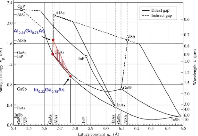
(28) Pseudomorphic HEMT. pHEMT consists of AlGaAs/InxGa1-xAs substructures on GaAs substrate with x <=0.3. Figure 2-3 shows the diagram of lattice constant about compound semiconductors.. Al0.24Ga0.76As. In0.22Ga0.78As. Figure 2-3 Bandgap versus lattice constant plots. For pseudomorphic high electron mobility transistors ( pHEMTs), InGaAs is used as channel material to increase the carrier transfer velocity. One of these limitations is the Al content x of the AlxGa1-xAs barrier layer should not be greater than about 0.3. The reason is that an increasing Al content will increase the donor activation energy EDA, thus leading to a more significant incomplete ionization and a lower doping efficiency. 7.
(29) Moreover, if x increases above 0.22, defects called DX centers are created and transistors. deteriorate.. Furthermore,. the. conduction. band. offsets. of. AlGaAs/InxGa1-xAs and InAlAs/InxGa1-xAs heterostructures are considerably larger than that of AlGaAs/GaAs. structures and increase with increasing x as well.. 2-2 Traditional HEMT Structure. 2-2-1 Cap layer. Usually the cap layer is heavily doped with silicon to form an excellent ohmic contact layer. This heavily doped layer reduces the drain (RD) and source electrode resistance (RS), it also prevents the Schottky layer from oxidation.. 2-2-2 Schottky layer. In order to make up 2-DEG to reduce impurity scattering, wide band gap material is grown on narrow band gap material, thus the Schottky layer is used for. 8.
(30) wide band gap, and it offers a high gate-to-drain diode characteristic to prevent the gate leakage current.. 2-2-3 δ-doping. The Schottky layer is usually heavily doped to 1018cm-3 level to get high carrier sheet density. However, the higher doping level decreases the gate breakdown voltage, which is not good for power application. One way to get high sheet density and breakdown voltage is planar doping or δ-doping. Usually the planar doping layer is a monolayer of Si with doping level about 5x1012cm-2 right above the spacer layer.. Now Schottky layer below the gate is undoped, which increases the breakdown voltage without decrease the sheet carrier density. Also the undoped schottky layer has much less leakage current and DX centers compared with the heavily doped one.. 2-2-4 Space layer. In HEMT’s channel, 2-DEG has a phenomenon which donors and electrons attract etch other, we called it coulomb scattering, in order to reduce coulomb scattering, we grow the spacer layer between barrier layer and channel layer. Typically the thickness of spacer layer is 20 Å~50 Å.. A spacer layer improves electro mobility and the breakdown voltage. On the other hand, a thin space layer increases the current and the higher transconductance 9.
(31) with lower doping in channel.. 2-2-5 Channel layer. To provide a 2-DEG with high mobility as well as electrons with good confinement, a narrow band gap material is used for the channel layer. The channel width is smaller than de Brogile wavelength (about 250Å at room temperature), so the energy bands are quantized.. 2-2-6 Buffer layer. Wide band gap materials, such as InAlAs or InAlGaAs, are generally used as buffer layer to prevent substrate leakage current. In HEMTs, the film is grown on semi-insulating substrates. Since there are many traps on the substrate, we grow a GaAs buffer layer between the substrate and the channel to reduce the interface roughness.. A superlattice structure buffer, stacking of wide and narrow band gap. material in terms, is also widely used for pHEMT.. 10.
(32) 2-3 Process Technology. In this chapter, we introduce fundamental process about compound semiconductor devices including mesa isolation, metal-semiconductor contact, gate recess and air bridge.. 2-3-1 Mesa Isolation. Normally first step of device fabrication is mesa isolation. As implied by the name “mesa isolation”, devices on the film were separated each other to control well-done current direction.. GaAs substrate have semi insulation characteristic, so we focus on other epitaxy layers like buffer layer. By using etch technology the parts around the device could be dismissed cleanly.. Besides having the advantage of devices were separated each. other, mesa isolation improved capability of controlling current direction. For HEMTs, mechanism of current controlling is that current flow into source from drain electrode by biasing in drain electrode. If the devices were not mesa isolated, current would not obey the rule so that it break devices’ performance. Besides, mesa isolation brings some additional advantage such as the reduction of the parasitic capacitance. When the gate metal contacts with semiconductor, it forms a Schottky barrier to arise a depletion region under gate electrode, it is called parasitic capacitance effect.. The. capacitance degree is proportional to the dimension of the metal pad, if we don’t separate active region with each other, the gate metal pad which situates on the 11.
(33) conductive epitaxy layer causes the parasitic capacitance effect which is greater than the capacitance under gate metal after mesa isolation. On the RF measurement, the parasitic capacitance effect reduces high frequency characteristic. Mesa isolation can reduce this effect and increase optimum the device’s performance.. 2-3-2 MS Contact. In the early 1900’s, the metal-semiconductor diode is one of compound semiconductor devices in the practical application, this diode also called point contact diode. The MS diodes are not be fabricated easily, and are not reliable devices, so in 1950’s,. it was replaced by pn junction . However, now the technology of. semiconductor and vacuum can fabricate extensive and reliable devices.. (a) Schottky Contact. The metal contacts with semiconductor, under the metal it produces a depletion region, it causes devices have rectification. Schottky contact (MS contact) is like to p+-n junction and being the diode characteristic.. (b) Ohmic Contact. A good ohmic contact display ideal linear character of I-V curve, more slope is large, more ohmic characteristic is desirable. 12.
(34) Figure 2-4(a) I-V curve of the Schottky contact. Figure 2-4(b) I-V curve of the ohmic contact. A good ohmic contact could be achieved mostly by three mechanisms as follows: 1. Thermionic Emission (TE) :. One way is by evaporating the narrow band gap metal that make a low barrier high , even if the carrier doping of the semiconductor is not large , electrons still can get cross the barrier easily by thermionic motion , we call the mechanism is thermionic emission . On the contrary, the barrier high is too large and the carrier concentration of the doping semiconductor is not large enough, electrons can not get cross the barrier by thermionic emission.. 13.
(35) 2. Field Emission (FE) :. Secondary way is that carrier concentration of doping layer is heavy (ND >1018/cm3) that the depletion width is narrow exceedingly, then electrons tunnel effect occurs. This mechanism is more significant than thermionic emission, The way of getting cross barrier is controlled by electrons tunnel motion, we call the mechanism is field emission.. Figure 2-5(a) Mechanism of TE motion. Figure 2-5(b) Mechanism of FE motion. 3. Thermionic-Field Emission (TFE). When doping carrier concentration Nd is less than 1018 /cm-3 but larger than 1017 /cm-3 , then the depletion width is not toomuch wide , thermionic and field emission mechanisms occur simultaneously . Figure 2-5 is shown as follows :. Figure 2-5(c) Mechanism of TFE motion. 14.
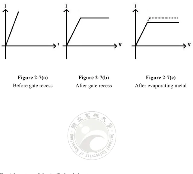
(36) 2-3-3 Gate Fabrication. Before gate metallization capping layer must be removed by wet etching. Usually the etching length which be recessed is longer than the gate length because of the undercut effect with the lateral etching.. then we use gate mask to define gate windows , and evaporate metal as a Schottky gate on the barrier layer, both sides of the metal do not contact with the cap layer to reduce parasitic capacitance effect , we called this way “self-Alignment” .. Figure 2-6 Ccross section of undercut. The depth of gate recessing for devices’ performance is an important parameter, the way to control the depth of gate recessing efficiently is to monitor the magnitude of the drain saturation current in the etching. process.. We observe that drain current was saturated and then was reduced with the increasing etching time by measuring the I-V characteristic of drain to source electrode , and stop etching until getting the drain current what we need . So the gate recess process is completed. 15.
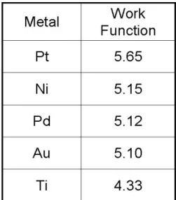
(37) Figure 2-7(a) Before gate recess. Figure 2-7(b) After gate recess. Figure 2-7(c) After evaporating metal. The Advantage of the Au/Pt-buried gate. Platinum (Pt) has shown a markedly high Schottky barrier height (> 0.83 eV) on the barrier layer making it an excellent candidate as a gate metal. Moreover, Pt reacts easily with As-based compound semiconductor during the annealing process and sinks into the semiconductor to a depth proportional to the platinum thickness.. Pt also sinks into the mesa sidewall of the narrow-gap channel and graded buffer layers. Little was paid to the kink-effect behavior and gate leakage when the Pt buried gate is formed by the annealing process. Table 2-1 shows each metal work function. 16.
(38) Table 2-1 Work functions of some widely used metals.. 2-3-4 Air Bridge. As implied by the name it is like a cross-over bridge to overcome the parasitic capacitance effect with metal conducting wires connecting crossly in IC design. Usually conducting wires connect gate metal with gate pad along the side wall of the device , so under the device the side wall have a MS contact to cause a depletion region , it bring the parasitic capacitance effect and against the device high frequency performance . Air bridge can reduce the dimension of MS contact under the device side wall , decrease the indifferent effect by the parasitic capacitance . Air bridge is shown as follows :. Figure 2-8 Air-bridge plot 17.
(39) Figure 2-9(a) Cross section of air-bridge. Figure 2-9(b) Plan view of air-bridge. 2-4 Device Fabrication. In this work, the pseudomorphic Al0.24Ga0.76As/In0.22Ga0.78As DH-HEMT structure was grown on a (100)-oriented semi-insulated GaAs substrate by molecular beam epitaxy (MBE) system. It consisted of a 0.5-µm undoped GaAs buffer, a 20-pair Al0.24Ga0.76As/In0.22Ga0.78As. (5-nm/5-nm). superlattice. sub-buffer,. a. 3.5-nm. n-Al0.24Ga0.76As (n=5×1018 cm−3) lower electron supply layer, a 5-nm Al0.24Ga0.76As lower spacer, a 12.5-nm undoped In0.22Ga0.78As channel, a 4.5-nm Al0.24Ga0.76As upper spacer, a δ(n+)-GaAs (δ(n+)=4×1012 cm−2) upper electron supply layer, a 30-nm undoped Al0.24Ga0.76As Schottky barrier, and finally a 35-nm n+-GaAs cap highly doped to n+=8×1018 cm−3 as shown in Figure 2-11. band diagram of the structure.. 18. Figure 2-10 shows the energy.
(40) Figure 2-10 Band diagram of DH-pHEMT. After removing the GaAs cap layer, Hall measurements indicate that the room-temperature carrier sheet density and electron mobility are 3.8×1012 cm−2 and 7850 cm2V−1s−1, respectively. Fabrication of the DH-HEMT was started with device mesa isolation. AuGe/Ni metals were deposited and were then lifted-off, thermally annealed as the drain/source ohmic electrodes with a spacing of 3 µm. After completely removing the cap through a 1-µm patterned photoresist window, Au/Pt (150-nm/5-nm) is directly deposited as the Schottky metal for forming air-bridge gates (named device A) [13]. One separated chip was further annealed in a N2 ambient at 280 oC for 5 minutes (device B) and another separated chip was at 330 oC for 5 minutes (device C). Figure 2-14 illustrates the cross-sectional view of a fabricated 19.
(41) DH-HEMT to simultaneously show an as deposited gate and a buried gate after annealing. Typical DC characteristics were measured by semiconductor parameter analyzer using on-wafer probing. Furthermore, the S-parameters, power performance, and noise figures of the fabricated DH-HEMTs with a total gate width of 100 µm were measured using on-wafer probing and a network analyzer (0.5 to 40 GHz for S-parameter, 2.4 GHz for power, and 1 to 8 GHz for noise).. n+-GaAs n=8x1018cm-3 i-Al0.24Ga0.76As i-Al0.24Ga0.76As GaAs. i-In0.22Ga0.78As. δ-doping. i-Al0.24Ga0.76As. 4x1012cm-3. n-Al0.24Ga0.76As n=5x1018cm-3 Al0.24Ga0.76As/GaAs S.L. Buffer Layer GaAs Buffer Layer ~ ~. S.I. GaAs Substrate. ~ ~. Figure2-11 Schematic cross section of the DH- pHEMT. 20.
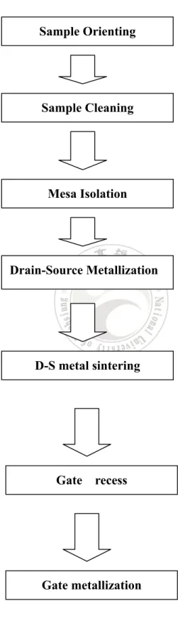
(42) Process procedure of HEMT. Sample Orienting. Sample Cleaning. Mesa Isolation. Drain-Source Metallization. D-S metal sintering. Gate. recess. Gate metallization. Figure 2-12 Process procedure of pseudomorphic HEMT. 21.
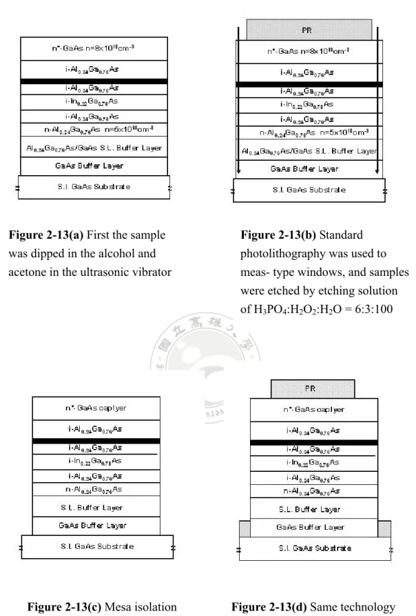
(43) Figure 2-13(a) First the sample was dipped in the alcohol and. Figure 2-13(b) Standard photolithography was used to. acetone in the ultrasonic vibrator. meas- type windows, and samples were etched by etching solution of H3PO4:H2O2:H2O = 6:3:100. Figure 2-13(c) Mesa isolation was completed.. Figure 2-13(d) Same technology to define drain-source type windows for metallization. 22.
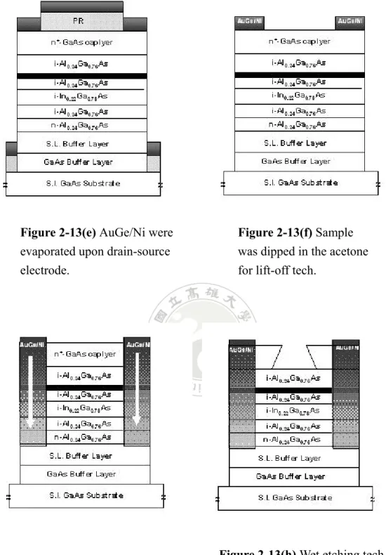
(44) Figure 2-13(e) AuGe/Ni were evaporated upon drain-source electrode.. Figure 2-13(f) Sample was dipped in the acetone for lift-off tech.. Figure 2-13(h) Wet etching tech. was used fore high selectivity solution by citric acid and gate recess tech. was used to dismiss the capping layer between Drain and Source and to gate. Figure 2-13(g) To get drain-source metal ohmic contact , we putted the sample on the hot-plate in the temperature for 300。C for 30 seconds.. metallization.. 23.
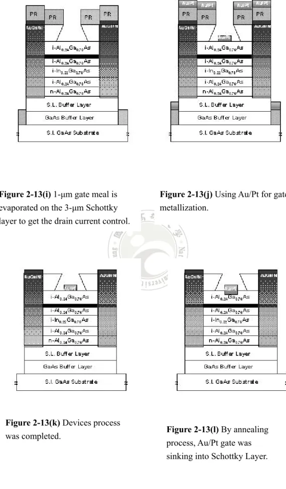
(45) Figure 2-13(i) 1-µm gate meal is evaporated on the 3-µm Schottky layer to get the drain current control.. Figure 2-13(j) Using Au/Pt for gate metallization.. Figure 2-13(k) Devices process was completed.. Figure 2-13(l) By annealing process, Au/Pt gate was sinking into Schottky Layer.. 24.
(46) Figure 2-14 Schematic cross-sectional view of fabricated DH-pHEMTs with a buried gate. 25.
(47) Chapter 3 Experimental Results and Discussion 3-1 DC Performance 3-1-1 Gate-drain Diode Characteristics. Figure 3-1 shows typical gate-drain current-voltage characteristics for the device A with an as deposited gate, the device B with a 280-℃ annealing gate, and the device C with a 330-℃ annealing gate. The turn-on voltages (Vons) defined at a forward gate current of IG = 1 mA/mm are 1.64, 1.72, and 1.76 V for device A, B, and C, respectively. The reverse gate leakage currents at VGS = −10 V are 81, 25, and 21 µA for devices A to C. Due to good carrier confinement at the Schottky/channel and the channel/buffer heterointerfaces, all devices show good Schottky characteristics. with high Vons and low IGs. Furthermore, devices B and C with an annealing gate exhibit breakdown voltages (defined at a IG = −1 mA/mm) of 13 and 13.5 V, which are larger than that (11 V) of device A with an as deposited gate.. Figure 3-1 Gate-drain current-voltage characteristics. 26.
(48) 3-1-2 Three Terminal I-V Characteristics. Kink Effect. For Ш-V microwave transistor , kink effect is a detrimental phenomenon , it results in increasing drain current , high output conductance , transconductance compression ,leading to reduced voltage gain and poor linearity , a threshold voltage shift . Several worker reported papers about mechanism of kink effect, and the physical origin of the effect is still a debated issue[7-9, 16-28]. At present three main interpretation proposed for kink effect are reported as follows: (1) impact ionization :. with increasing drain to source voltage , it generated. holes between drain and gate , where holes pile-up in the extrinsic source. result in. the threshold voltage shift , reduction of the source resistance , a slowly change of the surface charge and raising potential of the channel .[22-27] (2) traps : traping/detraping occurred in the deep level (3) include (1) and (2) : a combined effect of impact ionization and traping ,where generated holes modify the occupation state of channel surface , bulk of channel/substrate deep level .[8,9,28]. Shown in Figure 3-2 are the common-source characteristics for device A to C at room temperature. The device A exhibits an on resistance of 4 Ω·mm. Even though the Pt metal is annealed to sink into the Schottky barrier, the electron density in the 27.
(49) channel region between the source/drain and gate electrodes does not change. Both devices B and C exhibit nearly the same on resistance as that of the device A. This reveals that the series resistance between the source and gate electrodes is retained using buried-gate formation to control the threshold voltage. The kink behaviors generally taking place in the SH-HEMTs at negative VGSs are not observed for all fabricated devices. Clearly, our DH-HEMT structure with a bulk doping layer and superlattice sub-buffer underneath the channel is suitable for improving kink. However, a gradually reduced drain current is observed at VGS≥0 V and VDS≥3 V for devices A and B. It is believed to be due to the serious parallel conduction in the Schottky barrier layer.. Figure 3-2. Plot of three terminal I-V characteristic. 28.
(50) 3-1-3 Transconductance-Current Characteristics. Figure 3-3 shows the corresponding transfer characteristics (i.e., extrinsic transconductance and drain current as a function of VGS) for devices A to C. The Pt metal reacts easily with As-based compound semiconductors during the annealing process and sinks into the semiconductor to some depth. The sinking of Pt into the Schottky barrier shifted the gate metal front closer to the InGaAs channel, as illustrated in Figure 2-14.. It is thus found that the device A with an as deposited gate metal exhibits the maximum drain current (ID) of 475 mA/mm at VGS=+1 V. The drain currents at VGS=+1 V are reduced to 435 and 400 mA/mm after 280- and 330-℃ annealing for 5 minutes. It is thus found that the threshold voltage (VTH) defined as the VGS intercept of the extrapolation of a tangent from the ID at the point of maximum extrinsic transconductance (gm,max) are −2.35, −1.75 and −1.4 V for devices A, B, and C, respectively. Furthermore, there are two peaks in the gm vs. VGS characteristics for the device A. By annealing the Pt gate at 280 ℃ for 5 minutes, two enhanced peaks are positively shifted. The gm,max for a HEMT is related to the distance between the gate and Schottky metal (deff) and electron saturation velocity (υsat), which is typical expressed as:. g m, max. =. (Z × υ sa t × ε ) d eff. (1). 29.
(51) In the gm vs. VGS characteristics, one peak is due to electron carriers in the InGaAs channel and the other is due to electron carriers transferred into the δ(n+)-GaAs layer. On the other hand, the deff is reduced by sinking the Pt gate into the Schottky barrier. The smaller the deff is the larger the gm,max is. So, the gm,max of the device B is enhanced as compared to that of the device A. The device C with a 330-℃ annealing gate even displays a much broader plateau in the gm vs. VGS characteristics, showing the best charge control and device linearity of three devices. By fitting the ID versus VGS curve to study the device linearity, the polynomial for the device C is expressed as [15]:. ID = a0 + a1VGS + a2VGS2 + a3VGS3+ a4VGS4 + a5VGS5 + a6VGS6. (2). = 247.5 + 169.2VGS − 6VGS2 + 1.9VGS3 − 7.9VGS4 − 5VGS5 + 2.9VGS6. where a0 = 247.5 is the value of ID at VGS = 0 V and an’s are independent variables to determine the device linearity. Thus the voltage-dependent gm can also be described by a power series of the form:. gm(VGS) =. dID = gm0 + gm1VGS + gm2VGS2 + gm3VGS3 + gm4VGS4 + gm5VGS5 dVGS. = a1 + 2a2VGS + 3a3VGS2 + 4a4VGS3 + 5a5VGS4 +6a6VGS5. (3). Assuming a simple second-order nonlinearity and gm nonlinearity only (i.e. output conductance, gd=constant), we obtain the result. 30.
(52) a2Vg Second - harmonic gm1Vg = = fundamental 2gm0 a1. (4). and VGS = Vgcos(wt). (5). Table3-1 shows the comparison with device A, device B, and device C, the second-harmonic to fundamental ratio (a2/a1) at VGS = 0 V is 8.41 %, 9.29 % and3.55 %, respectively.. Table 3-1 Comparisons of the device linearity between device A, device B, and device C of the device linearity. Accordingly, the second-harmonic to fundamental ratio (a2/a1) at VGS = 0 V is as small as 3.55 %. Experimental results reveal that higher gms and better device linearity are obtained when the buried gate is used to determine the final distance between the gate and channel.. 31.
(53) Figure 3-3 Extrinsic transconductance and drain current as a function of VGS). 32.
(54) 3-1-4 Output Conductance Characteristics. Figure 3-4 shows the gm, gd, and open-drain voltage gain (Av = gm/gd) as a function of VDS for devices A to C at VGS = −1.0 V. The relatively low gds and high Avs are obtained. Note that no peaks are observed in gd versus VDS characteristics for devices A to C, indicating no kink. Under the applied bias condition of VGS = −1.0 V and VDS ≥ 2.0 V, the gd and gm are about 1.1 and 150 mS/mm for the device A, resulting in a Av of 136. On the other hand, Avs of 170 and 160 are obtained for devices B and C under the same bias condition. The higher Avs are attributed to the higher aspect ratio in devices B and C with a buried gate.. Figure 3-4 gm, gd, and open-drain voltage gain (Av = gm/gd) as a function of VDS. 33.
(55) 3-2 RF Characteristics 3-2-1 High Frequency Performance. The experimental microwave performances for devices A to C at VDS = 3 V are shown in Figure 3-5. Typically, the unity-current gain frequency (ft) is directly related to the gm and the total gate capacitance (CG). With decreasing the deff, both the gm and CG are increased. Thus the measured maximum fts of 13.5, 13.5 and 14.5 GHz for devices A, B, and C are compatible. However, devices B and C with a buried gate still exhibit a little higher fts and better frequency linearity than device A does in the range of −1.0 ≤VGS ≤ 0.25 V. The same trend in the fmax versus VGS characteristics is also obtained. The measured maximum fmaxs are 35, 37, and 37.5 GHz for the devices A, B, and C, respectively. Under the bias condition of the VDS = 3 V and VGS = −1.0 V, all devices exhibit a fmax/ft ratio of > 2.5 due to improved carrier confinement and low output conductance.. Figure 3-5 Experimental microwave performances for devices A to C at VDS = 3 V 34.
(56) 3-2-2 Power Characteristics. Shown in Figure 3-6 is the power performance of all devices A to C with a gate width of 100 µm at 2.4 GHz under VDS of 3.0 V and VGS of −1.0 V. The linear power gains are 16.5, 15, and 13.5 dB for devices A, B, and C. The quiescent current for device A, B, and C are about 19, 13, and 7 mA, respectively. Thus the corresponding peak PAEs of 37.3, 40.6, and 44.8 % with an associated output power (Pout) of 13.8, 12.5, and 10.7 dBm are found at an input power (Pin) of 4, 3, and 1 dBm, respectively. The saturation power densities are 256, 190, and 145 mW/mm for devices A, B, and C.. Figure 3-6 Power performance of all devices A to C with a gate. width of 100 µm at 2.4 GHz under VDS of 3.0 V and VGS of −1.0 V.. 35.
(57) 3-2-3 Noise Figure. Figure 3-7 shows the dependence of the noise figure and associated gain on the frequency. The frequency is in the range of 1.2 to 7.2 GHz with an interval of 0.6 GHz. The bias conditions are VDS = 3 V and VGS = −1.0 V for all devices. It is firstly found that the noise of all devices increased with the increase of the frequency. However, the device C exhibits the smallest values while the device A exhibits the largest ones in the whole frequency range. One of possible reasons for these results is due to the bias current (about 190, 130, and 70 mA/mm for devices A, B, and C, respectively). Another possible reason is due to the improved reverse gate leakage in the device C. Therefore, at 2.4 (7.2) GHz, a gain of 19.7 (11.7) dB can be obtained at the Fmin= 1.46 (3.32) dB for the device C with a 330-℃ annealing gate, while gains of 16.6 (10) and 18.6 (11) dB are obtained at the Fmin= 2.19 (4.04) and 1.64 (3.88) dB for devices A and B, respectively.. , Figure 3-7 Relation of the noise figure and associated gain on the frequency. 36.
(58) Chapter 4 Theoretical Analysis and Simulation. 4-1 Theory and Simulation In this chapter, the theoretical analysis and simulation are made by using a two-dimensional simulator Atlas. Based on the variations of the gate-metal sinking depth, the dc and rf performances are compared and studied. The pseudomorphic Al0.24Ga0.76As/In0.22Ga0.78As DH-HEMT structure used in the simulation and for practical device fabrication is listed in Table 4-1.. Table 4-1 Device structure of the studied DH- pHEMT in the theoretical analysis.. 37.
(59) A 2-D semiconductor simulation package Atlas was used to analyze the performance of DH-HEMT with a different sinking depth of gate metal [14], [15]. Five fundamental equations related to electron and hole current continuity, electron and hole concentrations, and Poisson’s equation are taken into account to simulate device performance. Other important physical mechanisms, such as Fermi-Dirac statistics,. Shockley-Read-Hall. recombination,. field-dependent. mobility,. and. concentration-dependent mobility are also included. The saturation velocities used for the InGaAs channel, δ-doped GaAs sheet, and AlGaAs layer are 1.5×10⁷, 1.1×10⁷, 6×106 cm/s, respectively. Figure 2-14 illustrates the cross-sectional view of the DH-HEMT with an as deposited gate metal upon the 300 Å undoped Al0.24Ga0.76As Schottky barrier. Shown in Figure 4-1 is the DH-HEMT with a sinking gate depth of h. The h’s used in the simulation are 50 and 75 Å, which are reasonable as considering the 50 Å Pt-metal deposition. All simulated data are for the devices with a gate dimension of 1×100 µm2.. Figure 4-1 The DH-HEMT with a sinking gate depth of h.. 38.
(60) 4-2 Simulation Results and Analysis 4-2-1 Band Diagrams of DH-HEMTs with Different Depth of Schottky Barrier Figures 4-2(a) to (c) illustrate the corresponding band diagrams of DH-HEMTs with a gate-metal sinking depth of h=0, 50, and 75 Å, respectively. The applied gate-source voltage (VGS) is swept from −1 to +1 V with 1 V per step. The reference origin of the depth axis is defined as the exposed surface of the AlGaAs Schottky barrier. For Figures 4-2(a) to (c) the difference is the effective thickness of the Schottky barrier underneath the sinking gate metal. Thus the aspect ratios are different from each other. One of key features for the DH-HEMT design is that the strained InGaAs channel with indium mole fraction as high as 0.22 is used to improve electron transport properties and confinement effects.. Figure 4-2(a) Band diagrams of DH-HEMT with a 300Å Schottky barrier,. As can be seen, the larger conduction-band discontinuity (∆EC∼0.34 eV) at the. 39.
(61) bottom heterojunction is beneficial for electrons in the channel from being injected and/or tunneled into sub-buffer/buffer layers at VGS=−1 V. The employed δ-doped sheet as the upper electron supply layer is expected to improve the parallel conduction when electrons in the channel are injected and/or tunneled back at positive VGSs.. Figure 4-2 (b) Band diagrams of DH-HEMT with a 250Å Schottky barrier,. Figure 4-2 (c) Band diagrams of DH-HEMT with a 225Å Schottky barrier, 40.
(62) 4-2-2 Electron Sheet Density. Shown in Figure 4-3(a) to (d) are electron densities for DH-HEMTs biased at VGS=+1 V, +0.5 V, 0 V, and −1 V, respectively. As seen in the Figure 4-3(c) with VGS=0 V, the DH-HEMT with a h=0 Å has the highest total electrons in the channel than others. The calculated electron sheet density is nearly equal to that of Hall measurement. So, the largest drain saturation current is obtained for DH-HEMT with a h=0 Å.. Figure 4-3 Electron sheet density of the device with h=0, 50, 75 Å biased at. VGS=+1 V, +0.5 V, 0 V, and −1 V 41.
(63) By applying a VGS of −1 V, the electron density of the DH-HEMT with a h=75 Å is abruptly reduced [see in Figure 4-3(d)]. In addition to better charge control, this. means that the threshold voltage of the DH-HEMT with a thicker gate-metal sinking depth shifts positively. With increasing VGS positively, the electrons in the channel start injecting and/or tunneling back to the δ-doped GaAs sheet, as shown in Figure 4-3 (c). Moreover, Figure 4-3 (a) with VGS=+1 V for the DH-HEMT with a h=0 Å even has their mass of electrons inject into AlGaAs Schottky barrier where poor transport properties there are.. Based on the analysis for electrons versus VGS, it is concluded that (i) sinking gate metal instead of thinning the Schottky barrier can be used to control the threshold voltage wanted, (ii) increasing aspect ratio of the DH-HEMT can further improve transconductance suppression and hence device linearity, and (iii) a higher turn-on voltage with a lower leakage is also expected by sinking gate-metal.. 42.
(64) 4-2-3 Calculated Current-Voltage Characteristics. Figure 4-4 shows calculated common-source output current-voltage (I-V) characteristics of the devices studied: DH-HEMTs with a gate-metal sinking depth of 0, 50, 75 Å. Excellent pinch-off and saturation characteristics are found for all devices. Clearly, due to the good carrier confinement in the In0.22Ga0.78As channel, the devices can be operated at a positive VGS larger than +1 V. A higher current is obtained in the DH-HEMT with a h=0 Å. This result is consistent with the phenomena observed in Figure 4-4. Furthermore, at VGS=+1 V and VDS=0 to +0.5 V, the on-resistances are nearly the same for all devices. Unlike a recessed gate, a sinking gate has its electron density in the channel region between the source/drain and gate electrodes unchanged. This is suggested that the series resistance between the source and gate electrodes is retained by sinking gate metal to control the threshold voltage.. Figure 4-4 I-V characteristics of the devices studied: DH-HEMTs with a gate-metal sinking depth of 0, 50, 75 Å 43.
(65) 4-2-4 Transconductance Characteristics. Figure 4-5 shows corresponding transfer characteristics (i.e., drain current and transconductance as a function of VGS) for all devices. The drain-source voltage is fixed at VDS=4 V. Calculated drain currents at VGS=0 V (+1 V) are355 (508), 293 (469), and253 (444) mA/mm for the DH-HEMTs with a h=0, 50, and 75 Å, respectively. The threshold voltage (VTH) as a function of gate-metal sinking depth is also included as an inset. The VTH linearly increases from −2.07 to −1.31 V when the gate-metal sinking depth is in the range of 0 to 75 Å. The shifting factor of the threshold voltage is about 10 mV/ Å. In addition, the corresponding maximum values of transconductance are 171, 186, and 197 mS/mm. The transconductance is directly related to the distance between the gate electrode and the channel. The shorter the distance is the larger the transconductance is. Thus it is reasonable that the DH-HEMTs with a h=75 Å exhibits the highest transconductance of the three.. Figure 4-5 Transfer characteristics as a function of VGS 44.
(66) In order to investigate effects of the gate-metal sinking depth on device linearity, the ID versus VGS curve can be fitted by polynomial and be expressed as [15]:. ID = a0 + a1VGS + a2VGS2 + a3VGS3+ a4VGS4 + a5VGS5 + a6VGS6 +……. (1). where a0 and a1 are the values of ID and gm at VGS =0 V and an’s (n≥2) are independent variables to determine the device linearity. Assuming a simple second-order nonlinearity and gm nonlinearity only (i.e. output conductance, gd=constant), we obtain the result Second - harmonic a2Vg = fundamental a1. (4). and VGS = Vgcos(wt). (5). Table 4-2 lists the corresponding values of a0, a1, and a2 for DH-HEMTs with a h=0, 25, 50, and 75 Å, indicating good fitting results to the ID and gm at VGS = 0 V. Accordingly, the second-harmonic to fundamental ratio (a2/a1) at VGS = 0 V is only 6.7 % for the DH-HEMT with a h=0 Å. By increasing the gate-metal sinking depth to 75 Å, the second-harmonic to fundamental ratio is even as small as 0.92 %. Clearly, the improvement is due to a higher aspect ratio by sinking gate metal.. Table 4-2 Second-harmonic to fundamental ration (a2/a1) of the devices with a sinking gate-metal gate h = 0, 25, 50, and 75Å 45.
(67) 4-2-5 Output Conductance and Voltage Gain Characteristics. Figure 4-6 shows output conductance (gd) and open-drain voltage gain (Av) as a function of VDS. The biased VGS is fixed at −0.5 V for all devices. It is found that DH-HEMT with a thicker gate-metal sinking depth exhibits a smallest output conductance and a largest associated voltage gain. At a VDS=5 V, calculated gd’s (Av’s) are 6.5 (26), 5.0 (37), and 4.1 (45) mS/mm for DH-HEMTs with a h=0, 50, and 75 Å, respectively. Again, this reveals that a higher aspect ratio provides better charge control and offers a higher voltage gain.. Figure 4-6 Output conductance (gd) and open-drain voltage gain (Av) as a function of VDS. On the other hand, the unity-current gain frequency (ft) is typically related to the gm and the total gate capacitance (CG) and is expressed as:. 46.
(68) fT ≈. gm 2π Cgs. (6). With decreasing the effective distance between the gate electrode and the channel, both the gm and Cgs are increased. Thus the gate-metal sinking depth (and hence the aspect ratio) should play very little effect on ft. However, without considering the parasitic effects, the unity power-gain frequency (fmax) can be approximately expressed as:. f max ≈. fT 2 Ri g d. (7). where Ri is the channel resistance. Since the gd is improved by increasing the aspect ratio, the DH-HEMT with a thicker gate-metal depth is expected to show an enhanced fmax. Figure 4-7 shows ft and fmax as a function of VGS. The biased VDS is 3 V for all. devices.. Figure 4-7 ft and fmax as a function of VGS 47.
(69) Chapter 5 Conclusion For the upper electron supply layer, the Schottky metal is deposited is not necessary to be highly doped. Thus a high breakdown voltage is available and also a low output conductance thanks to the additional bottom heterojunction. This additional bottom heterojunction in the DH-HEMTs can be served as a barrier to prevent the electrons from being injected into the buffer. Kink-free current-voltage characteristics are also expected. The experimental results with a buried gate (different depth) are compared in table5-1.. Table 5-1 The experimental results with a buried gate (different depth). In the aspect of simulation, the results also demonstrate that the higher and more 48.
(70) linear transconductance characteristics, lower leakage currents, and larger voltage gains were obtained due to the increasing aspect ratio by a buried gate. Furthermore, detailed AC performance and comparison were also investigated. Experimental and calculated results reveal the same conclusion that the buried gate formation is another better approach to control DH-HEMT performance when compared with the recessed gate.. Expectation. In the conclusion, a buried gate technology is used to control the threshold voltage. Obviously, enhancement-mode HEMT can be obtained by Au/Pt gate annealing process if Vth > 0. Therefore, we can design a high speed logic circuit by using E/D mode HEMTs. In the other way, Reliability of the HEMT with a buried gate in high temperature is an important studied subject in the feature.. 49.
(71) References [1] L. D. Nguyen, A. S. Brown, M. A. Thompson, and L. M. Jelloian, “50-nm self-aligned-gate pseudomorphic AlInAs/GaInAs high electron mobility transistors,” IEEE Trans. Electron Devcies, vol. 39, no. 9, pp.2007-2014, Sep. 1992. [2] D. W. Tu, S. W. Duncan, A. Eskandarian, B. Golja, B. C. Kane, S. P. Svensson, S. Weinreb, and N. E. Byer, “High gain monolithic W-band low noise amplifiers based on pseudomorphic high electron mobility transistors,” IEEE Trans. Microwave Theory and Techniques, vol. 42, pp.2590-2597, Dec. 1994. [3] Y. J. Jeon, Y. H. Jeong, B. Kim, Y. G. Kim, W. P. Hong, and M. S. Lee, “DC and RF performance of LP-MOCVD grown Al0.25Ga0.75As/InxGa1-xAs (x=0.15-0.28) P-HEMT with Si-delta doped GaAs layer,” IEEE Electron Device Lett., vol.16, pp.563-565, Dec. 1995. [4] H. M. Shieh, W. C. Hsu, T. T. Hsu, C. L. Wu, and T. S. Wu, “A high-performance δ-doped GaAs/InxGa1-xAs pseudomorphic high electron mobility transistor utilizing a graded InxGa1-xAs channel,” IEEE Electron Device Lett., vol.14, pp.581-583, Dec. 1993. [5] S. Arai and H. Tokuda, “Millimeter-wave power HEMTs,” Solid-State Electron., vol.41, pp.1575-1579, Oct. 1997. [6] K. H. Yu, H. M. Chuang, K. W. Lin, S. Y. Cheng, C. C. Cheng, J. Y. Chen, and W. C. Liu, “Improved temperature-dependent performances of a novel InGaP-InGaAs-GaAs double channel pseudomorphic high electron mobility transistor (DC-PHEMT),” IEEE Trans. Electron Devices, vol.49, pp.1687-1693, Oct. 2002. [7] A. thmasian, A. A. Rezazadeh, and L. G. Hipwood, “Observation and mechanism of kink effect in depletion-mode AlGaAs/GaAs and AlGaAs/InGaAs HEMTs,” Electron. Lett., vol.25, pp.351-352, Mar. 1989. [8] J. Haruyama, H. Negishi, Y. Nishimura, and Y. Nashimoto, “Substrate-related kink effects with a strong light-sensitivity in AlGaAs/InGaAs PHEMT,” IEEE Trans..
數據
+7

相關文件
Programming languages can be used to create programs that control the behavior of a. machine and/or to express algorithms precisely.” -
a single instruction.. Thus, the operand can be modified before it can be modified before it is used. Useful for fast multipliation and dealing p g with lists, table and other
• If a graph contains a triangle, any independent set can contain at most one node of the triangle.. • We consider graphs whose nodes can be partitioned into m
The main advantages of working with continuous designs are (i) the same method- ology can be essentially used to find continuous optimal designs for all design criteria and
The hashCode method for a given class can be used to test for object equality and object inequality for that class. The hashCode method is used by the java.util.SortedSet
Now, nearly all of the current flows through wire S since it has a much lower resistance than the light bulb. The light bulb does not glow because the current flowing through it
Corpus-based information ― The grammar presentations are based on a careful analysis of the billion-word Cambridge English Corpus, so students and teachers can be
It is the author’s hope that the Zuting shiyuan may be effectively used as a supplement for understanding Chan texts, and its contributions be fully valued.. Furthermore, the
