次世代快閃記憶體之氨氣氮化底多晶矽上多晶矽層間高介電常數介電質特性
67
0
0
全文
(2) 次世代快閃記憶體之氨氣氮化底多晶矽上 多晶矽層間高介電常數介電質特性 Characteristics of the Inter-Poly High-κ Dielectrics on NH3-Nitrided Bottom Poly-Si for Next Generation Flash Memories 研 究 生:李宗翰. Student : Tsung-Han Li. 指導教授:羅正忠 博士. Advisors : Dr. Jen-Chung Lou. 國 立 交 通 大 學 電子工程學系 電子研究所 碩 士 論 文 A Thesis Submitted to Institute of Electronics College of Electrical Engineering and Computer Science National Chiao Tung University in Partial Fulfillment of the Requirements for the Degree of Master of Science in Electronic Engineering June 2005 Hsinchu, Taiwan, Republic of China. 中華民國 九十四 年 六 月.
(3) 摘要. 次世代快閃記憶體之氨氣氮化底多晶矽上 多晶矽層間高介電常數介電質特性. 研究生 : 李宗翰. 國立交通大學. 指導教授 : 羅正忠 博士. 電子工程學系. 電子研究所. 摘要. 隨著系統晶片(SOC)的發展,持續降低互補式金氧半(CMOS)場效電晶 體元件中的閘極介電層及非揮發性記憶體(non-volatile memories)中的複晶矽層 間介電層(inter-poly dielectric)厚度以提高元件密度及降低操作電壓變得十分重 要。為了滿足以上的需求並獲得較低的漏電流及較高的可靠度,利用高介電常數 材料(high-κ)來取代二氧化矽(SiO2)變成是不可或缺的趨勢。 本篇論文研究沉積後高溫退火(post-deposition annealing)溫度對有機金屬 化學氣相沉積(metal organic chemical vapor deposition)之高介電常數材料三氧 化二鋁(Al2O3)及二氧化鉿(HfO2)複晶矽層間電容的影響。實驗結果顯示, 對三氧化二鋁及二氧化鉿複晶矽層間電容,不論是漏電流、電子捕捉率或崩潰電 荷,900oC和 800oC分別是最佳化條件。因此,等效氧化層厚度為 5 奈米及 3 奈 米的三氧化二鋁和二氧化鉿將是 45 奈米及 32 奈米世代以下堆疊式快閃記憶體的 絕佳候選複晶矽層間介電質。 -I-.
(4) ABSTRACT. Characteristics of the Inter-Poly High-κ Dielectrics on NH3-Nitrided Bottom Poly-Si for Next Generation Flash Memories. Student : Tsung-Han Li. Advisors : Dr. Jen-Chung Lou. Department of Electronics Engineering & Institute of Electronics National Chiao-Tung University. Abstract. For the system-on-chip (SOC) application, a continuously scaling of the gate dielectrics for complementary metal oxide semiconductor (CMOS) and inter-poly dielectrics. (IPDs). for. electrically-erasable. programmable. read-only-memory. (EEPROM) and stacked-gate flash memory is needed to obtain high density and low operation voltage. To meet the above requirements and exhibit low leakage current as well as good reliability, the replacement of high-κ materials for SiO2 have become indispensable. In this thesis, we investigated the effects of post-deposition annealing (PDA) temperature on the electrical properties and reliability characteristics of metal-organic chemical vapor deposition (MOCVD) aluminum oxide (Al2O3) and hafnium oxide (HfO2) inter-poly capacitors. For Al2O3 and HfO2 inter-poly capacitors, samples - II -.
(5) ABSTRACT. exhibit optimal quality in terms of leakage current, electron trapping rate and charge-to-breakdown (QBD) when annealed at 900oC and 800oC respectively. As thin as 5nm and 3nm equivalent oxide thickness (EOT) of Al2O3 and HfO2 IPD is suitable to meet the requirement of 45nm and 32nm generation stacked-gate flash memories respectively.. - III -.
(6) 誌謝. 誌. 謝. 兩年的碩士生涯終於在認真忙碌的學習與同學的歡笑聲中結束 了,首先要感謝我的指導教授羅正忠博士,在老師諄諄教誨與勉勵之 下,讓我在做人做事與學術研究上都有了受益終身的收穫與啟發,特 此向羅老師呈上最衷心的感謝。另外要特別感謝陳永裕、陳世璋、謝 文斌三位學長,謝謝你們在學業與專業研究上提供這許許多多的指導 與協助,在生活中如兄長般的照顧與關愛更讓我感到無比的溫暖,當 實驗遇到困難時不遺餘力地幫我解決問題,讓我順利地完成了研究所 的課業。還要感謝彥廷、祐慈、昶維、雁雅、明衡以及其他實驗室的 同學,也感謝國源、佳寧還有各位學弟,兩年來大家一起努力,互相 幫助,更共同擁有歡樂的時光,我知道這將是我人生中美好的回憶。 在這裡也要對國家奈米實驗室以及裡面勞苦功高的研究人員、工程師 們致上深深的謝意,因為你們熱心地提供專業的意見與幫助,讓實驗 能順利的進行。 最後要對我的父母、家人說聲謝謝,這麼多年來,你們總是默默 耕耘,讓我沒有後顧之憂地完成我的學業,雖然你們從未提起片言隻 字,卻讓我深深體會到這份親情的可貴與感動,謝謝你們。. - IV -.
(7) CONTENTS. Contents. Abstract (in Chinese) ............................................................................................... I Abstract (in English) ................................................................................................ II Acknowledgements ................................................................................................. IV Contents ................................................................................................................... V Table Captions ......................................................................................................... VII Figure Captions ....................................................................................................... VIII. Chapter 1 Introduction ........................................................................................... 1 1.1. Background ...................................................................................................... 1. 1.2. Motivation ........................................................................................................ 4. 1.3. Organization of the Thesis ................................................................................ 8. Chapter 2 Effects of PDA Temperature on the Electrical Properties of Al2O3 IPD with NH3 nitridation .................................................................... 13 2.1. Introduction .................................................................................................... 13. 2.2. Experimental Details ...................................................................................... 14. 2.3. Results and Discussions ................................................................................. 15. 2.3.1. Basic Electrical Properties ........................................................................ 15. 2.3.2. Electric Field and Leakage Current Density Characteristics ………….... 16. 2.3.3. Reliability Characteristics ........................................................................ 16. 2.4. Summary ........................................................................................................ 18. -V-.
(8) CONTENTS. Chapter 3 Effects of PDA Temperature on the Electrical Properties of HfO2 IPD with NH3 nitridation ………………………………………….... 27 3.1. Introduction .................................................................................................... 27. 3.2. Experimental Details ...................................................................................... 29. 3.3. Results and Discussions ................................................................................. 30. 3.3.1. Basic Electrical Properties ........................................................................ 30. 3.3.2. Electric Field and Leakage Current Density Characteristics .................... 30. 3.3.3. Reliability Characteristics ........................................................................ 31. 3.4. Summary ........................................................................................................ 32. Chapter 4 Conclusions and Recommendations for Future Works …………... 43 4.1. Conclusions .................................................................................................... 43. 4.2. Recommendations for Future Works .............................................................. 44. References ................................................................................................................. 46. - VI -.
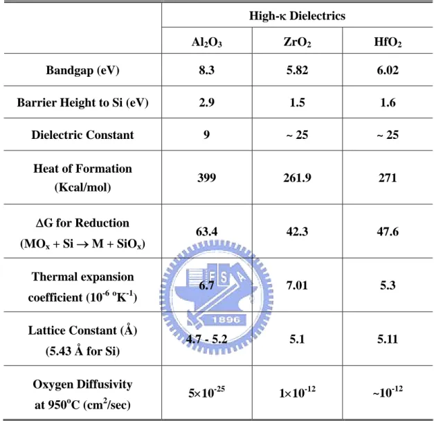
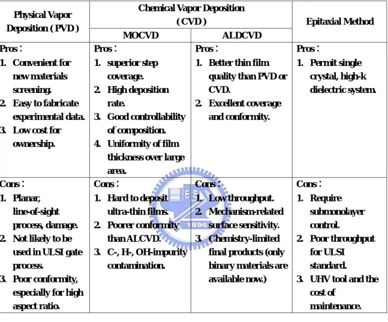
(9) TABLE CAPTIONS. Table Captions. Chapter 1 Table 1.1 Materials properties of high-κ dielectrics, Al2O3, ZrO2 and HfO2 Table 1.2 Comparisons of deposition technique: sputtering, ALD, MOCVD and MBE. Chapter 2 Table 2.1 EOT, effective breakdown field, 6MV/cm-biased leakage current density and 63%-failure QBD values of the Al2O3 inter-poly capacitors with surface NH3 nitridation under positive and negative CCS at various PDA temperatures in N2 ambient. Chapter 3 Table 3.1 EOT, effective breakdown field, 6MV/cm-biased leakage current density and 63%-failure QBD values of the HfO2 inter-poly capacitors with surface NH3 nitridation under positive and negative CVS at various PDA temperatures in N2 ambient. Chapter 4 Table 4.1 Comparison of 800ºC PDA HfO2 IPD and 900ºC PDA with 900ºCPEA Al2O3 IPD samples in terms of EOT, effective breakdown field, 6MV/cm-biased leakage current density and 63%-failure QBD values. - VII -.
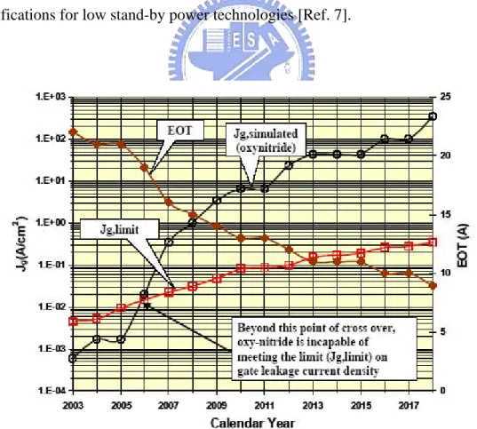
(10) FIGURE CAPTIONS. Figure Captions. Chapter 1 Fig. 1.1. Scaling limits of various gate dielectrics as a function of the technology specifications for low stand-by power technologies.. Fig. 1.2. Leakage current density and EOT projection of nitrided oxides from ITRS roadmap 2004 update.. Fig. 1.3. A schematic diagram of typical MOCVD system structure.. Chapter 2 Fig. 2.1. Cross-sectional view of Al2O3 inter-poly capacitors with surface NH3 nitridation and post-deposition nitrogen annealing.. Fig. 2.2. Key process steps of Al2O3 inter-poly capacitors with surface NH3 nitridation and post-deposition nitrogen annealing.. Fig. 2.3. (a) C-V curves and (b) J-E characteristics of Al2O3 inter-poly capacitors with surface NH3 nitridation and post-deposition nitrogen annealing.. Fig. 2.4. The Weibull distributions of the effective breakdown field of Al2O3 inter-poly capacitors with surface NH3 nitridation and post-deposition nitrogen annealing under (a) positive and (b) negative polarities.. Fig. 2.5. The Weibull distributions of the leakage current density of Al2O3 inter-poly capacitors with surface NH3 nitridation and post-deposition nitrogen annealing under (a) positive and (b) negative polarities as the gate bias is 6MV/cm.. Fig. 2.6. (a) QBD Weibull distributions and (b) the corresponding curves of gate voltage shift of Al2O3 inter-poly capacitors with surface NH3 nitridation at various PDA temperatures when CCS of 5mA/cm2 is applied in positive polarity.. Fig. 2.7. (a) QBD Weibull distributions and (b) the corresponding curves of gate voltage shift of Al2O3 inter-poly capacitors with surface NH3 nitridation at various PDA temperatures when CCS of 5mA/cm2 is applied in negative polarity.. Fig. 2.8. Band diagrams of Al2O3 inter-poly capacitors with surface NH3 nitridation under (a) positive and (b) negative gate voltage biased to the Poly-II.. - VIII -.
(11) FIGURE CAPTIONS. Chapter 3 Fig. 3.1. Band alignment of typical high-κ dielectrics.. Fig. 3.2. Cross-sectional view of HfO2 inter-poly capacitors with surface NH3 nitridation and post-deposition nitrogen annealing.. Fig. 3.3. Key process steps of HfO2 inter-poly capacitors with surface NH3 nitridation and post-deposition nitrogen annealing.. Fig. 3.4. (a) C-V curves and (b) J-E characteristics of HfO2 inter-poly capacitors with surface NH3 nitridation and post-deposition nitrogen annealing.. Fig. 3.5. Equivalent oxide thickness of HfO2 inter-poly capacitors with surface NH3 nitridation and post-deposition nitrogen annealing.. Fig. 3.6. Comparison of EOT between Al2O3 and HfO2 inter-poly capacitors with surface NH3 nitridation and post-deposition nitrogen annealing.. Fig. 3.7. The Weibull distributions of the effective breakdown field of HfO2 inter-poly capacitors with surface NH3 nitridation and post-deposition nitrogen annealing under (a) positive and (b) negative polarities.. Fig. 3.8. The Weibull distributions of the leakage current density of HfO2 inter-poly capacitors with surface NH3 nitridation and post-deposition nitrogen annealing under (a) positive and (b) negative polarities as the gate bias is 6MV/cm.. Fig. 3.9. The Weibull distributions of the leakage current density of HfO2 inter-poly capacitors with surface NH3 nitridation and post-deposition nitrogen annealing under (a) positive and (b) negative polarities as the gate bias is 5V.. Fig. 3.10 QBD Weibull distributions of HfO2 inter-poly capacitors with surface NH3 nitridation at various PDA temperatures under (a) positive and (b) negative polarities. Fig. 3.11 Curves of gate current density shift of HfO2 inter-poly capacitors with surface NH3 nitridation and post-deposition nitrogen annealing under (a) positive and (b) negative constant voltage stress.. - IX -.
(12) CHAPTER 1: INTRODUCTION. CHAPTER 1 Introduction. 1.1 Background. As the scaling rule keeps going, the dimension of gate oxide for complementary metal oxide semiconductor (CMOS) has decreased dramatically for the past decade. The integrated circuit technology nowadays makes devices with high density and low operation voltage for the system-on-chip (SOC) application. To meet such requirements like high performance (speed), low static (off-state) power and a wide range of power supply and output voltages [1], we have to perform a calculated reduction of the dimensions of the fundamental active device in the circuit just like what “Moore’s law” indicated, doubling the circuit density about every two or three years since 1980 [2]-[4]. And this trend results in a dramatic expansion in technology and communication markets including the market associated with high-performance microprocessor and low static-power applications, such as wireless systems. Just like what we already knew, the key element of keeping the scaling rule of Si-based metal-oxide-semiconductor field effect transistor (MOSFET) going is the materials and resultant electrically properties associated with the dielectric employed to isolate the transistor gate from the Si channel for decades: silicon dioxide (SiO2). We can benefit several key advantages in CMOS processing including a thermodynamically and electrically stable high-quality Si-SiO2 interface as well as superior electrical -1-.
(13) CHAPTER 1: INTRODUCTION. isolation properties by using thermally grown amorphous SiO2 as the gate dielectric. ~1010 cm-2 defect charge density, ~1010 cm-2eV-1 midgap interface state density and 15 MV/cm hard breakdown field are routinely obtained and therefore expected in spite of dimensions. These outstanding electrical properties clearly present a significant challenge for any other alternative gate dielectric candidates [5], [6]. As the time past, there have been several major evolutions in silicon digital logic technology. CMOS technology became the most important digital logic technology for all IC industry, owing to its low standby power dissipation and scaling potential. The scaling of oxide thickness has long been recognized as one of determinant factor for devices scaling. High driving current and thereby improved performance can be achieved by reducing the oxide thickness. At the current rate of progressing, Fig. 1.1 indicates the imperative need for a nitrided oxide (SiOxNy) and high dielectric constant (κ) gate dielectrics for low standby power application after the year 2002 and 2006, respectively [7]. However, the direct tunneling current increases exponentially by about one order of magnitude for every 0.2nm ~ 0.3nm reduction in oxide thickness. This additional leakage current not only causes increased power dissipation but also affect the circuit functionality due to the decreased operation margins. For this reason, several alternative materials for silicon dioxide are currently being investigated. Ultrathin nitrided oxides are, at this moment, the best choices to replace pure SiO2 [8]-[14]. Figure 1.2 shows the expected equivalent oxide thickness (EOT) trends from the published 2004-ITRS roadmap. It indicated that nitrided oxides can extend SiO2 limitation to 2006 without massive change in production technologies. Nitrided oxides have several properties superior to those of conventional thermal SiO2, and it deserves to mention the suppression of boron penetration from the poly-Si gate and enhanced reliability. Nitrogen also reduces hot-electron-induced degradation [15]. -2-.
(14) CHAPTER 1: INTRODUCTION. The dielectric constant of the oxynitride increases linearly with the percentage of nitrogen from κ (SiO2) = 3.9 to κ (Si3N4) = 7.8 [16], though one should note that most SiOxNy films grown currently by thermal methods are lightly doped with N (< 10 at.%) and therefore have a dielectric constant only slightly higher than that of pure SiO2. The other potential candidates to replace silicon dioxide are high-κ materials, including aluminum oxide (Al2O3), hafnium oxide (HfO2) and zirconium oxide (ZrO2) etc [17]-[20]. The most important advantage of high-κ dielectric is the several orders reduction of magnitude of leakage current compared to SiO2 at the same EOT. However, in device performance point of view, a suitable gate dielectric candidate should also meet the other requirements, including high thermal stability, high carrier mobility, small oxide charges, good stress immunity and CMOS compatible. On the other hand, high-κ dielectrics are paid much attention on the flash memory applications [21]-[27].The thickness of inter-poly dielectric (IPD) and tunnel dielectric (TD) in stacked-gate flash memory had met intrinsic limitation [28]. It is not sufficient to meet the stringent data retention requirement of IPD while applying thermal or CVD oxynitride technologies due to the unavoidable leakage current [29]-[32]. By increasing the floating gate coupling ratio, high-κ IPD can lead to a high electric field across tunnel oxide (TOX) even at very low control gate voltage. For the tunnel dielectric engineering of stacked-gate flash memories, the issue is closely related to dielectric material selection itself. Flash tunnel dielectric has two roles. One is a barrier to suppress charge leakage under read and retention. Second role is a charge transfer path. In order to avoid trap-assisted tunneling via one trap site, the minimum TOX thickness of conventional FG structure will be limit to 8 nm. This limits the tunnel SiO2 scaling and program/erase voltage reduction. Nitrided oxides have been intensively studied, but so far only 5 to 10 times improvement for low field. -3-.
(15) CHAPTER 1: INTRODUCTION. leakage is achieved [33]. This is not enough, because it only achieves 1 nm reduction even with heavy nitridation. To successfully employ the high-κ IPD and TD into flash memory, one must take charge retention issues into consideration and make sure that the barrier height (ϕB) between Si and the new adopted high-κ dielectrics should be larger than 1.5eV for effectively suppressing the loss of floating gate charges through electron thermal emission [33]. Usually, dielectrics with higher κ inherently have lower ϕB. Therefore a trade-off between dielectric constant and barrier height is inevitably required in trying to implement the high-κ dielectrics in flash memories.. 1.2 Motivation. Fast low-power nonvolatile memories are required for future wireless communication products. In the recent flash memory technologies, short program/erase times and operating voltage reductions are the most important issues to realize high speed/low power operation [28], [34]-[36]. For EEPROM and flash memory devices, the IPD requires a high charge-to-breakdown (QBD), high breakdown field and low leakage current to obtain good data retention characteristics [37]-[39]. It is not sufficient to meet the stringent data retention requirement of IPD while applying thermal or CVD oxynitride technologies due to the unavoidable leakage current [29]-[32], [40]. In order to accomplish this without a trade-off between low power and high speed operations, high coupling ratio should be achieved by increasing the floating gate capacitance [34], [35], [41]-[48]. There are three different approaches can be used to increase coupling ratio. First, -4-.
(16) CHAPTER 1: INTRODUCTION. decrease the IPD thickness. Oxide/nitride/oxide (ONO) multi-layered films had been extensively investigated and frequently used as the dielectric layer in the flash memory devices and other applications [49]-[51]. However, decreasing the thickness of the IPD to increase the coupling ratio may cause serious leakage and reliability problems which are fatal in the retention time of flash memories. Secondly, increase the area of the IPD capacitor. High capacitive-coupling ratio cell [41]-[43], 3-dimension inter-poly dielectric [45], and hemisphere grain [46], [47] had been proposed to effectively increase the capacitance area and lower the control gate bias. Although the coupling ratio of above mentioned cell structure could be dramatically improved, they must be fabricated with many additional process steps for fabrication such complex structures and be difficult to control well. The final approach is to increase the dielectric constant (κ) of IPD materials [22], [23], [27], [52]-[59]. Therefore, it is straightforward and effective to incorporate alternative high dielectric constant (high-κ) materials on nonvolatile memories to replace oxide/nitride/oxide IPD for increasing floating gate capacitance without increasing cell area and complexity of fabrication while suppressing charge loss. By increasing the floating gate coupling ratio, high-κ IPDs can lead to a high electric field across tunnel oxide even at very low control gate voltage. Recently, aluminum oxide (Al2O3) [17], [60]-[62] and hafnium oxide (HfO2) [20], [63]-[66] had been proved as promising candidates for the gate dielectrics of sub-0.1 µm device due to their higher κ, relatively high ϕB and superior thermal stability, shown in Table 1.1. Thanks to the high dielectric constant and high thermal stability, Al2O3 and HfO2 are suitable to be integrated into stacked-gate flash memories. Nonetheless, the effects of these kinds of high-κ dielectrics on flash memories are seldom investigated. To further realize the dielectric properties of these. -5-.
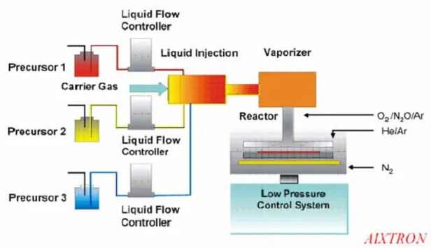
(17) CHAPTER 1: INTRODUCTION. high-κ dielectrics, some reliability issues such as breakdown field, charge trapping and temperature-dependence behaviors are extensively studied for both gate dielectric and flash memories applications. Many deposition methods such as physical vapor deposition (PVD), metal-organic chemical vapor deposition (MOCVD), atomic layer chemical vapor deposition (ALCVD) [67], [68], and molecular beam epitaxial method (MBE), etc. have been employed to prepare high-κ IPDs. The pros and cons of each deposition techniques are demonstrated in Table 1.2. For industrial application, PVD and MBE are not appropriate tools for high-κ film deposition. Since MOCVD has the advantage of superior step coverage, high deposition rate, good controllability of composition, excellent uniformity of film thickness over large area, we, therefore, choose the MOCVD technology as our tool to deposit thin high-κ IPDs. A detail schematic structure is shown in Fig. 1.3. The MOCVD chamber is equipped with a turbomolecular. pump. and. a. liquid. injection. system,. which. has. four. independent-controlled injectors. The latter is consisted of a liquid pump to pump the precursors through a hot nickel frit with a proper rate because the pump is unreliable at low pump rates. The vapors are carried with a 200sccm flow of Ar to a gas distribution ring which is located at a proper distance from the substrate. In contrast to the conventional bubble system, the liquid injection is with sufficient temperature window to alleviate the thermal aging of the precursor. This is because the precursor remains in liquid state at room temperature until it is pumped into the vaporizer and injected into the deposition chamber. However, the precursor should be kept at long-term chemical stability in solvent and non-reactive with other precursors solvent [69], [70]. The components of the vaporizer, the gas ring and the connecting tube are maintained at a temperature of 190ºC with heating tapes and blankets, while the. -6-.
(18) CHAPTER 1: INTRODUCTION. substrate temperature is controlled at 500ºC with quartz-halogen lamps and a thermocouple. A rotating suspensor is used for uniform heating during processing. A flow of 100sccm N2 is maintained throughout the deposition cycle. The base pressure of the MOCVD chamber is ~10-8Torr. The deposition pressure of the deposition is at the 5mTorr where the gas-phase collisions are scarce. As many reports indicated, the direct contact of high-κ materials and Si-substrate will be imperfect and debatable. The dominance of the Si MOSFETs over competing technologies has largely been attributed to the high quality of thermally grown SiO2 and the resulting Si/SiO2 interface [71]. The Si/SiO2 interface is known to have a very low density of interface states (Dit~2×10¹⁰ ststes/cm2) arising from unsaturated surface bonds and other electrically active imperfections [71]. Interface states lead to degradation of on-current, since carrier mobility is limited by scattering at the interface due to the strong vertical electric field present in the channel. For maintaining the excellent transport properties at the Si interface, a possible method to suppress the interfacial layer thickness is to passivate the Si surface before the high-κ IPD deposition. Generally, there are many methods to passivate the Si surface such as surface nitridation, nitrogen-contained ambient annealing, or nitride deposition as the bottom layer. Nitridation of the Si surface using NH3 treatment before the deposition of high-κ materials has been shown to be effective in achieving the low EOT and preventing the boron penetration [72], [73]. However, this technique results in higher interface charges which leads to higher hysteresis and reduced channel mobility [74]. The NH3 treatment would nitridize the Si surface to form a silicon nitride layer [75]-[77]. Silicon nitride is a superior barrier for H2O and oxygen, and it can suppress oxygen to diffuse into Si substrate [72]. After the NH3 treatment, a thin silicon nitride ( SixNy ) layer ( ~10 Å ) was deposited and measured by optical measurement system ( Ellipsometer ). As reports, nitridation of the Si surface is prior to the deposition of -7-.
(19) CHAPTER 1: INTRODUCTION. high-κ gate dielectrics and it shows the result to achieve the low EOT and increase reliability by making the interface smoother [78].. 1.3 Organization of This Thesis. There are four chapters in this thesis. In chapter 1, we present a conceptive introduction to describe the background of the semiconductor technology and discuss the possible issues that we may meet during the dimension scaling down. In addition, we would concern about the hopeful solutions to overcome the physical limits in the ITRS, discuss and explain the reasons for high-κ IPD application in the nonvolatile flash memories. In chapter 2, the effects of post-deposition annealing (PDA) temperature on inter-poly characteristics of MOCVD Al2O3 dielectrics are examined. The basic electrical properties, electric field, leakage current, and reliability characteristics are presented and discussed. In chapter 3, the effects of PDA temperature on inter-poly characteristics of MOCVD HfO2 dielectrics are examined. The basic electrical properties, electric field, leakage current, and reliability characteristics are presented and discussed. Finally, in chapter 4, the conclusions are made and the recommendations describe the topics which can be further researched.. -8-.
(20) CHAPTER 1: INTRODUCTION. Table 1.1 Materials properties of high-κ dielectrics, Al2O3, ZrO2 and HfO2.. High-κ Dielectrics Al2O3. ZrO2. HfO2. Bandgap (eV). 8.3. 5.82. 6.02. Barrier Height to Si (eV). 2.9. 1.5. 1.6. Dielectric Constant. 9. ~ 25. ~ 25. Heat of Formation (Kcal/mol). 399. 261.9. 271. 63.4. 42.3. 47.6. 6.7. 7.01. 5.3. 4.7 - 5.2. 5.1. 5.11. 5×10-25. 1×10-12. ~10-12. ∆G for Reduction (MOx + Si → M + SiOx) Thermal expansion coefficient (10-6 oK-1) Lattice Constant (Å) (5.43 Å for Si) Oxygen Diffusivity o. 2. at 950 C (cm /sec). -9-.
(21) CHAPTER 1: INTRODUCTION. Table 1.2 Comparisons of deposition techniques: sputtering, ALD, MOCVD and MBE.. Chemical Vapor Deposition ( CVD ). Physical Vapor Deposition ( PVD ). MOCVD. Epitaxial Method. ALDCVD. Pros:. Pros:. Pros:. Pros:. 1. Convenient for new materials screening. 2. Easy to fabricate experimental data. 3. Low cost for ownership.. 1. superior step coverage. 2. High deposition rate. 3. Good controllability of composition. 4. Uniformity of film thickness over large area. Cons:. 1. Better thin film quality than PVD or CVD. 2. Excellent coverage and conformity.. 1. Permit single crystal, high-k dielectric system.. Cons:. Cons:. Cons: 1. Planar, line-of-sight process, damage. 2. Not likely to be used in ULSI gate process. 3. Poor conformity, especially for high aspect ratio.. 1. Hard to deposit 1. Low throughput. ultra-thin films. 2. Mechanism-related 2. Poorer conformity surface sensitivity. than ALCVD. 3. Chemistry-limited 3. C-, H-, OH-impurity final products (only contamination. binary materials are available now.). - 10 -. 1. Require submonolayer control. 2. Poor throughput for ULSI standard. 3. UHV tool and the cost of maintenance..
(22) CHAPTER 1: INTRODUCTION. Fig. 1.1 Scaling limits of various gate dielectrics as a function of the technology specifications for low stand-by power technologies [Ref. 7].. Fig. 1.2 Leakage current density and EOT projection of nitrided oxides from ITRS roadmap 2004 update.. - 11 -.
(23) CHAPTER 1: INTRODUCTION. Fig. 1.3 A schematic diagram of typical MOCVD system structure.. - 12 -.
(24) CHAPTER 2: EFFECTS OF Al2O3 PDA TEMPERATURE. CHAPTER 2 Effects of PDA Temperature on the Electrical Properties of Al2O3 IPD with NH3 Nitridation. 2.1 Introduction. With the scaling down of thickness of the inter-poly dielectrics (IPD), the quality of the dielectric becomes very critical for the application of the EEPROM and Flash nonvolatile memories. Lower leakage of the dielectric means longer data retention time. As many reports indicated that high-κ IPDs with surface NH3 nitridation have been shown improved electrical properties [21]-[23]. Among those potential candidates, aluminum oxide (Al2O3) is the most attractive for IPD application in nonvolatile flash memories because of its higher conduction band offset with respect to the underlying poly-Si electrode and its higher permittivity with respect to Si3N4 [17], [21], [57], [71], [79], [80]. On the other hand, it is found that the incorporation of nitrogen on the bottom poly-Si surface can not only reduce leakage current by one order of magnitude, but also enhance the breakdown field and the charge-to-breakdown (QBD) as well [23]. This is ascribed to the resultant smoother interface between the dielectric and the floating gate by surface nitridation and less electron traps in the bulk [23]. However, the QBD is unfortunately quite low. Moreover, the effects of post-deposition annealing (PDA) temperature on the electrical properties. - 13 -.
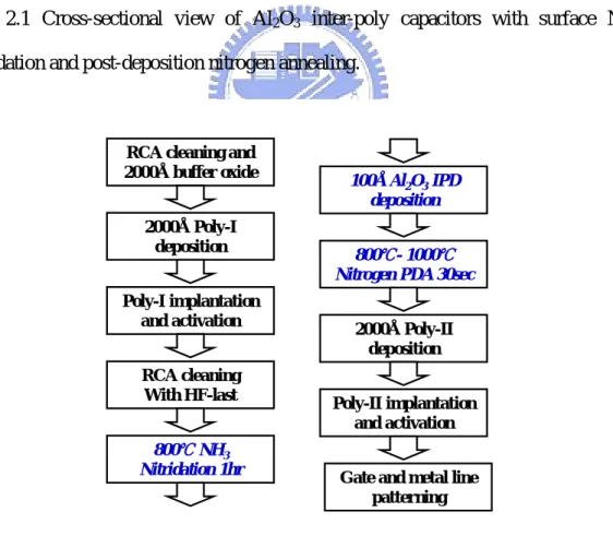
(25) CHAPTER 2: EFFECTS OF Al2O3 PDA TEMPERATURE. and reliability characteristics of MOCVD Al2O3 inter-poly capacitors with surface NH3 nitridation are studied in this chapter. The electrical properties of the Al2O3 IPD are influenced by the PDA temperature. The optimum is 900ºC Al2O3 IPD in terms of leakage current, electron trapping rate and QBD.. 2.2 Experimental Details. The n+-polysilicon/Al2O3 IPD/n+-polysilicon capacitors were fabricated on 6-inch p-type (100)-oriented silicon wafers. Silicon wafer was thermally oxidized at 950ºC to grow a 2000Å buffer oxide. 2000Å bottom polysilicon film (Poly-I) was deposited on the buffer oxide by low pressure chemical vapor deposition (LPCVD) system using SiH4 gas at 620ºC and subsequently implanted with phosphorous at 5e15cm-2, 20keV, then activated with RTA at 950ºC for 30s. Prior to the growth of Al2O3 IPDs, the native oxide covering Poly-I was cleaned by the conventional RCA cleaning and diluted HF etching in sequence for the removal of particles and native oxides. The surface of Poly-I prepared in this matter was known to be contamination-free and terminated with atomic hydrogen. After being wet cleaned and dipped in HF solution, all samples were subjected to ammonia (NH3) nitridation in the LPCVD furnace at 800ºC for 1 hour. Then, 10nm Al2O3 IPDs were deposited by MOCVD system at 500ºC. Annealing of Al2O3 IPDs was carried out by rapid thermal annealing (RTA) at temperatures ranging from 800ºC to 1000ºC in an N2 atmosphere for 30s. Subsequently, a 2000Å top polysilicon layer (Poly-II) was deposited by LPCVD system and implanted with phosphorous at 5e15cm-2, 20keV. Dopants were then activated with RTA at 950ºC for 30s. Finally, 5000Å TEOS oxide passivation and. - 14 -.
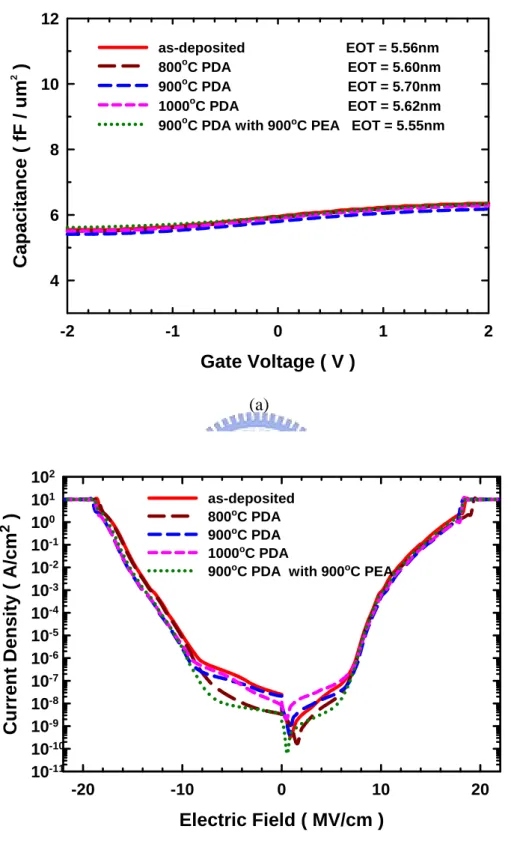
(26) CHAPTER 2: EFFECTS OF Al2O3 PDA TEMPERATURE. Al metal pads were defined. It is worthy to mention that we took one of the 900ºC PDA samples annealed again at 900ºC in N2 atmosphere followed by the dry etching step, called post-etching annealing (PEA). The cross-sectional view and key process steps of Al2O3 inter-poly capacitor with surface NH3 nitridation and post-deposition nitrogen annealing are shown in Figs. 2.1 and 2.2, respectively. The equivalent oxide thickness (EOT) was obtained from the high frequency (10 kHz) capacitance-voltage (C-V) measurement using a Hewlett-Packard (HP) 4284 LCR meter. The electrical properties and reliability characteristics of the inter-poly capacitors were measured using a HP4156C semiconductor parameter analyzer.. 2.3 Results and Discussions. 2.3.1 Basic Electrical Properties Figure 2.3 (a) shows the high frequency C-V curves (10kHz) and the corresponding EOT of Al2O3 inter-poly capacitors with surface NH3 nitridation annealed at 800ºC to 1000ºC. The EOT increases as PDA temperature rising up to 900ºC, which can be ascribed to the thick interfacial layer (IL) growth. As the PDA temperature continually increases to 1000ºC, in spite of the thickest IL, Al2O3 film may partially crystallize and slightly increase permittivity, smaller EOT value is therefore obtained as compared to 900ºC PDA samples. However, the differences of the EOT among these samples are less than 3Å, which can be ascribed to both the effects of surface NH3 nitridation and extremely low oxygen diffusivity of Al2O3 film. Figure 2.3 (b) presents the J-E characteristics of the Al2O3 inter-poly capacitors with NH3 nitridation at various PDA temperatures under both polarities. It is found that the. - 15 -.
(27) CHAPTER 2: EFFECTS OF Al2O3 PDA TEMPERATURE. large leakage current of 1000ºC PDA sample may be the proof of crystallization. We also found that 900ºC PDA with additional 900ºC post-etching annealing (PEA) sample can effectively reduce the low-field leakage current than other samples, which is helpful to suppress charge loss from the floating gate. It can be explained by the reduced damage generated by ion bombardment during the Poly-II patterning. In addition, it is worthy to mention that polarity dependence can be observed in gate leakage current curves, the leakage current in negative polarity is smaller than that in positive polarity due to asymmetric band diagram.. 2.3.2 Electric Field and Leakage Current Density Characteristics Figure 2.4 shows the breakdown characteristics of Al2O3 inter-poly capacitors with NH3 nitridation at various PDA temperatures under both polarities. Effective breakdown field exhibits nearly independent on PDA temperatures. Figure 2.5 compares the Weibull distributions of the leakage current of Al2O3 inter-poly capacitors at various PDA temperatures with NH3 nitridation in both polarities as the magnitude of gate bias is 6MV/cm. Once again, 1000ºC PDA sample has large leakage current caused by partially crystallization, and 900ºC PDA with 900ºC PEA sample has better performance in preventing charge loss from floating gate.. 2.3.3 Reliability Characteristics Figure 2.6 demonstrates (a) QBD Weibull distributions and (b) the corresponding curves of gate voltage shift of Al2O3 inter-poly capacitors with surface NH3 nitridation at various PDA temperatures when constant current stress of 5mA/cm2 is applied in positive polarity. In Fig. 2.6 (a), the smaller QBD value of 1000ºC PEA sample in - 16 -.
(28) CHAPTER 2: EFFECTS OF Al2O3 PDA TEMPERATURE. positive polarity is attributed to its thicker interfacial layer. The interfacial layer becomes thicker when post-deposition annealing temperature rises, then the voltage drop across interfacial layer will increase and result in stronger electric field. The increase in the gate voltage indicates that the primary mechanism responsible for the long-term wear-out in Al2O3 film is the creation of electron traps under positive polarity, as shown in Fig. 2.6 (b). We also found that Al2O3 inter-poly capacitors annealed at 900ºC with additional 900ºC PEA exhibits smaller trapping rate than other conditions and this phenomenon indicates improved film quality ,which is consistent with the result of suppressed gate leakage current shown in Fig. 2.3. We believe that additional 900ºC post-etching annealing can reduce damage generated by ion bombardment during the Poly-II patterning and further improve Al2O3 inter-poly capacitors characteristics such as leakage current and stress-induced trapping rate. However, it is totally different situation in negative polarity. Figure 2.7 shows (a) QBD Weibull distributions and (b) the corresponding curves of gate voltage shift of Al2O3 inter-poly capacitors with surface NH3 nitridation at various PDA temperatures when constant current stress of 5mA/cm2 is applied in negative polarity. In Fig. 2.7 (a), although thickness of interfacial layer increases as PDA temperature rising, there is no apparent difference in QBD for negative polarity. This fact reveals that the thickness of Al2O3 film dominate breakdown mechanism, i.e. bulk breakdown. In Fig. 2.7 (b), hole trapping is observed, which can ascribed to the electron-hole pairs generation caused by electron impact after injection from Poly-II to Poly-I under negative bias. Then holes jumped to valence band and were trapped in the Al2O3 bulk when they injected back to Poly-II. Such mechanism is called anode hole injection (AHI) [81], [82]. The other mechanism for hole trapping is injection of accumulation hole of Poly-I. The similar trapping rate in negative polarity is in agreement with the result of identical charge-to-breakdown as shown in Fig. 2.7 (a). Band diagrams of Al2O3 inter-poly - 17 -.
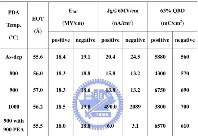
(29) CHAPTER 2: EFFECTS OF Al2O3 PDA TEMPERATURE. capacitors with surface NH3 nitridation under (a) positive and (b) negative gate voltage biased to the Poly-II are demonstrated in Fig. 2.8 (a) and (b) respectively.. 2.4 Summary. The effects of PDA temperature on the electrical properties and reliability characteristics of the Al2O3 inter-poly capacitors with surface NH3 nitridation are evaluated in this chapter. It was found that the electrical properties of Al2O3 IPD strongly depend upon the PDA temperature. 900ºC annealing is the best condition for the Al2O3 IPD electrical characteristics in terms of leakage current, trapping rate and QBD. Moreover, additional post-etching annealing is beneficial to improve Al2O3 thin film quality because it can reduce the defects generated during the Poly-II patterning. The results apparently demonstrate Al2O3 IPD with surface nitridation, optimized PDA temperature and another 900ºC PEA can effectively reduce charge transfer between control gate and floating gate, better retention and disturb characteristics are expected by replacing ONO IPD to Al2O3 IPD. The Al2O3 dielectric with surface NH3 nitridation, 900ºC post-deposition and post-etching annealing thus appears to be very promising for future flash memory devices. Table 2.1 lists several physical and electrical parameters, including EOT, effective breakdown field, 6MV/cm-biased leakage current density and 63%-failure QBD values of the Al2O3 IPDs with surface NH3 nitridation annealed at various temperatures.. - 18 -.
(30) CHAPTER 2: EFFECTS OF AL2O3 PDA TEMPERATURE. Table 2.1 EOT, effective breakdown field, 6MV/cm-biased leakage current density and 63%-failure QBD values of the Al2O3 inter-poly capacitors with surface NH3 nitridation under positive and negative CCS at various PDA temperatures in N2 ambient.. EBD. Jg@6MV/cm. 63% QBD. (MV/cm). (nA/cm2). (mC/cm2). PDA EOT Temp. (Å) (ºC). positive. negative. positive. negative. positive. negative. As-dep. 55.6. 18.4. 19.1. 20.4. 24.5. 5880. 560. 800. 56.0. 18.3. 18.8. 15.8. 13.2. 4300. 570. 900. 57.0. 18.3. 18.6. 13.8. 13.2. 6750. 690. 1000. 56.2. 18.5. 19.0. 490.0. 2089. 3800. 700. 55.5. 18.0. 18.8. 6.0. 3.1. 6570. 610. 900 with 900 PEA. - 19 -.
(31) CHAPTER 2: EFFECTS OF AL2O3 PDA TEMPERATURE. Al Metal Pad. TEOS 5000Å. 100Å Al2O3 SiNx ~10Å. 2000Å n+ Poly-II 2000Å n+ Poly-I 2000Å Buffer Oxide P-type Si Substrate. Fig. 2.1 Cross-sectional view of Al2O3 inter-poly capacitors with surface NH3 nitridation and post-deposition nitrogen annealing.. RCA cleaning and 2000Å buffer oxide 2000Å Poly-I deposition. 100Å Al2O3 IPD deposition 800℃- 1000℃ Nitrogen PDA 30sec. Poly-I implantation and activation RCA cleaning With HF-last. 2000Å Poly-II deposition Poly-II implantation and activation. 800℃ NH3 Nitridation 1hr. Gate and metal line patterning. Fig. 2.2 Key process steps of Al2O3 inter-poly capacitors with surface NH3 nitridation and post-deposition nitrogen annealing.. - 20 -.
(32) CHAPTER 2: EFFECTS OF AL2O3 PDA TEMPERATURE. 2. Capacitance ( fF / um ). 12 as-deposited 800oC PDA 900oC PDA 1000oC PDA 900oC PDA with 900oC PEA. 10. EOT = 5.56nm EOT = 5.60nm EOT = 5.70nm EOT = 5.62nm EOT = 5.55nm. 8. 6. 4 -2. -1. 0. 1. 2. Gate Voltage ( V ). Current Density ( A/cm2 ). (a). 102 101 100 10-1 10-2 10-3 10-4 10-5 10-6 10-7 10-8 10-9 10-10 10-11. as-deposited 800oC PDA 900oC PDA 1000oC PDA 900oC PDA with 900oC PEA. -20. -10. 0. 10. 20. Electric Field ( MV/cm ) (b) Fig. 2.3 (a) C-V curves and (b) J-E characteristics of Al2O3 inter-poly capacitors with surface NH3 nitridation and post-deposition nitrogen annealing.. - 21 -.
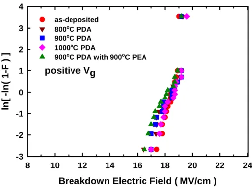
(33) CHAPTER 2: EFFECTS OF AL2O3 PDA TEMPERATURE. 4 as-deposited 800oC PDA 900oC PDA 1000oC PDA 900oC PDA with 900oC PEA. ln[ -ln( 1-F ) ]. 3 2. positive Vg. 1 0 -1 -2 -3 8. 10. 12. 14. 16. 18. 20. 22. 24. Breakdown Electric Field ( MV/cm ) (a) 4 as-deposited 800oC PDA 900oC PDA 1000oC PDA 900oC PDA with 900oC PEA. ln[ -ln( 1-F ) ]. 3 2 1. negative Vg. 0 -1 -2 -3 8. 10. 12. 14. 16. 18. 20. 22. 24. Breakdown Electric Field ( MV/cm ) (b) Fig. 2.4 The Weibull distributions of the effective breakdown field of Al2O3 inter-poly capacitors with surface NH3 nitridation and post-deposition nitrogen annealing under (a) positive and (b) negative polarities. - 22 -.
(34) CHAPTER 2: EFFECTS OF AL2O3 PDA TEMPERATURE. 4. ln[ -ln( 1-F ) ]. 3 2 1. positive Vg. 0. as-deposited 800oC PDA 900oC PDA 1000oC PDA 900oC PDA and PEA. -1 -2 -3 10-10. 10-9. 10-8. 10-7. 10-6. 10-5. 10-4. 10-3. Gate Leakage Current Density@6MV/cm ( A/cm2 ) (a). 4. ln[ -ln( 1-F ) ]. 3 2 1 0. negative Vg as-deposited 800oC PDA 900oC PDA 1000oC PDA 900oC PDA PEA. -1 -2 -3 10-10. 10-9. 10-8. 10-7. 10-6. 10-5. 10-4. 10-3. Gate Leakage Current Density@6MV/cm ( A/cm2 ) (b) Fig. 2.5 The Weibull distributions of the leakage current density of Al2O3 inter-poly capacitors with surface NH3 nitridation and post-deposition nitrogen annealing under (a) positive and (b) negative polarities as the gate bias is 6MV/cm. - 23 -.
(35) CHAPTER 2: EFFECTS OF AL2O3 PDA TEMPERATURE. 4 as-deposited 800oC PDA 900oC PDA o 1000 C PDA 900oC PDA and PEA. 3. ln[ -ln( 1-F ) ]. 2 1. CCS@Jg = 5mA/cm2. 0 -1 -2 -3 -4 0.1. 1. 10. 100. Charge to Breakdown ( C/cm2 ) (a). 0.6 2. Gate Voltage Shift ( V ). CCS@Jg= + 5mA/cm 0.5 0.4 0.3 0.2. as-deposited 800oC PDA 900oC PDA 1000oC PDA 900oC PDA with 900oC PEA. 0.1 0.0 0. 10. 20. 30. 40. 50. 60. 70. 80. 90 100 110. Time ( sec ) (b) Fig. 2.6 (a) QBD Weibull distributions and (b) the corresponding curves of gate voltage shift of Al2O3 inter-poly capacitors with surface NH3 nitridation at various PDA temperatures when CCS of 5mA/cm2 is applied in positive polarity. - 24 -.
(36) CHAPTER 2: EFFECTS OF AL2O3 PDA TEMPERATURE. 4 3. ln[ -ln( 1-F ) ]. 2 1 0. CCS@Jg = - 5mA/cm2. -1. as-deposited 800oC PDA 900oC PDA 1000oC PDA 900oC PDA and PEA. -2 -3 -4 0.1. 0.2 0.30.4 0.5 0.6 0.7 0.8 0.9 1. 2 3 4 5 678910. 20 30405060 78 090 100 0. Charge to Breakdown ( C/cm2 ) (a). 0.30. Gate Voltage Shift ( V ). CCS@Jg= - 5mA/cm. 2. 0.25 as-deposited 800oC PDA 900oC PDA 1000oC PDA 900oC PDA with 900oC PEA. 0.20 0.15 0.10 0.05 0.00 0. 10. 20. 30. 40. 50. 60. 70. 80. 90 100 110. Time ( sec ) (b) Fig. 2.7 (a) QBD Weibull distributions and (b) the corresponding curves of gate voltage shift of Al2O3 inter-poly capacitors with surface NH3 nitridation at various PDA temperatures when CCS of 5mA/cm2 is applied in negative polarity. - 25 -.
(37) CHAPTER 2: EFFECTS OF AL2O3 PDA TEMPERATURE. Positive Vg -. -. -. -. - -. -. Poly-I. - - - - - - - - - - Poly-II Al2O3 IPD I.L.. (a). Negative Vg -- -- -- -. Poly-II. + +. +. +. +. impact ionization -+. + +. Poly-I. + +. Al2O3 IPD. + + + + ++. I.L.. (b) Fig. 2.8 Band diagrams of Al2O3 inter-poly capacitors with surface NH3 nitridation under (a) positive and (b) negative gate voltage biased to the Poly-II.. - 26 -.
(38) CHAPTER 3: EFFECTS OF HfO2 PDA TEMPERATURE. CHAPTER 3 Effects of PDA Temperature on the Electrical Properties of HfO2 IPD with NH3 Nitridation. 3.1 Introduction. Recently, HfO2 has gained much attention as promising insulator. The reasons are briefly listed as follows. (1) Suitable high dielectric constant: The reported dielectric constant of HfO2 is about 25~30. This magnitude of κ-value is higher than that of Si3N4 (κ~7) and Al2O3 (κ=8~11.5). It is not high enough to induce severe fringing-induced barrier lowering effect. (2) Wide bandgap: In general, as the dielectric constant increases, the bandgap decreases. The narrower bandgap would increase leakage current through thermal emission. The energy bandgap of HfO2 is about 5.68eV, which is higher than the other high-κ materials such as ZrO2, Si3N4 and Ta2O5. (3) Acceptable band alignment: Band alignment determines the barrier height for electron and hole tunneling. - 27 -.
(39) CHAPTER 3: EFFECTS OF HfO2 PDA TEMPERATURE. from gate or Si substrate. For SiO2 the band offset of conduction band and valence band is ~9eV, and the barrier height for electrons is 3.1eV and the barrier height for holes is 4.7eV. The high band offset for both electron and hole has the benefit of low leakage current. Figure 3.1 shows the calculated band offsets for most high-κ dielectrics [83]. For HfO2, barrier height for electron and hole is 1.6eV and 3.3eV, respectively. This band alignment is acceptable for nonvolatile memory requirement and better than other high-κ materials such as Ta2O5 [33]. (4) High free energy of reaction with Si: For HfO2, the free energy of reaction with Si is about 47.6 kcal/mole at 727ºC (see Table 1.1), which is higher than that of TiO2 and Ta2O5. Therefore, HfO2 is a more stable material on Si substrate as compared to TiO2 and Ta2O5. (5) High heat of formation: Among the elements in IVA group of the periodic table (Ti, Zr, Hf), Hf has the highest heat of formation (271 kcal/mole). Unlike other silicides, the silicide of Hf can be easily oxidized. And it means that Hf is easy to be oxidized to form HfO2 and the oxide of Hf is usually stable on Si substrate. (6) Superior thermal stability with poly-Si: Unlike ZrO2, HfO2 shows a good thermodynamic stability with poly-Si [84], [85]. The HfO2 would not react easily with poly-Si in high temperature as ZrO2 [86].. According to these profits discussed above, we choose HfO2 as one of the major high-κ IPDs in our investigation for next decade flash memories.. - 28 -.
(40) CHAPTER 3: EFFECTS OF HfO2 PDA TEMPERATURE. 3.2 Experimental Details. The n+-polysilicon/HfO2 IPD/n+-polysilicon capacitors were fabricated on 6-inch p-type (100)-oriented silicon wafers. Silicon wafer was thermally oxidized at 950ºC to grow a 2000Å buffer oxide. 2000Å bottom polysilicon film (Poly-I) was deposited on the buffer oxide by low pressure chemical vapor deposition (LPCVD) system using SiH4 gas at 620ºC and subsequently implanted with phosphorous at 5e15cm-2, 20keV, then activated with RTA at 950ºC for 30s. Prior to the growth of HfO2 IPDs, the native oxide covering Poly-I was cleaned by the conventional RCA cleaning and diluted HF etching in sequence for the removal of particles and native oxides. The surface of Poly-I prepared in this matter was known to be contamination-free and terminated with atomic hydrogen. After being wet cleaned and dipped in HF solution, all samples were subjected to ammonia (NH3) nitridation in the LPCVD furnace at 800ºC for 1 hour. Then, 10nm HfO2 IPDs were deposited by MOCVD system at 500ºC. Annealing of HfO2 IPDs was carried out by rapid thermal annealing (RTA) at temperatures ranging from 600ºC to 1000ºC in an N2 atmosphere for 30s. Subsequently, a 2000Å top polysilicon layer (Poly-II) was deposited by LPCVD system and implanted with phosphorous at 5e15cm-2, 20keV. Dopants were then activated with RTA at 950ºC for 30s. Finally, 5000Å TEOS oxide passivation and Al metal pads were defined. The cross-sectional view and key process steps of HfO2 inter-poly capacitor with surface NH3 nitridation and post-deposition nitrogen annealing are shown in Figs. 3.2 and 3.3, respectively. The equivalent oxide thickness (EOT) was obtained from the high frequency (10kHz) capacitance-voltage (C-V) measurement using a Hewlett-Packard (HP) 4284 LCR meter. The electrical properties and reliability characteristics of the inter-poly - 29 -.
(41) CHAPTER 3: EFFECTS OF HfO2 PDA TEMPERATURE. capacitors were measured using a HP4156C semiconductor parameter analyzer.. 3.3 Results and Discussions. 3.3.1 Basic Electrical Properties Figure 3.4 (a) and (b) show the high frequency C-V curves (10kHz) and the current density-effective electric field (J-E) characteristics of HfO2 inter-poly capacitors with surface NH3 nitridation annealed at 600ºC to 1000ºC, respectively. The low capacitance and suppressed leakage current of 1000ºC PDA sample can be ascribed to its thicker EOT, shown in Fig. 3.5. Lower post-deposition annealing temperature won’t cause large difference in the oxygen diffusivity between HfO2 and Al2O3 film. When annealing temperature is high as up to 1000ºC, due to the high oxygen diffusion coefficient of HfO2, shown in Table 1.1, oxygen can easily penetrate the HfO2 film and react with the layer beneath HfO2 film to form thick interface layer. This effect can be clearly observed in Fig. 3.6. Compared to the low oxygen diffusivity of Al2O3 film, oxygen can penetrate all the way through HfO2 film to form interface layer at high temperature. So, the higher the post-deposition annealing temperature is, the thicker the interface will be formed. As HfO2 is not a good oxygen diffusion barrier, the control of oxygen concentration and temperature would be very critical when we apply HfO2 film as the inter-poly dielectric in production line.. 3.3.2 Electric Field and Leakage Current Density Characteristics Figure 3.7 depicts the Weibull distributions of the effective breakdown field of HfO2 inter-poly capacitors with surface NH3 nitridation and post-deposition nitrogen - 30 -.
(42) CHAPTER 3: EFFECTS OF HfO2 PDA TEMPERATURE. annealing under (a) positive and (b) negative polarities. In both polarities, the effective breakdown field of the 800ºC PDA annealed HfO2 IPD is obviously higher than those of as-deposited and 600ºC PDA samples. And we believe this is due to the improved thin film quality of 800ºC PDA sample. Since HfO2 IPD annealed at 1000oC will oxidize underlying Poly-I more effective than others, both large effective breakdown field and degraded Weibull slope can be explained by thicker interfacial layer and poor interface morphology. Figure 3.8 demonstrates the Weibull distributions of the leakage current of HfO2 inter-poly capacitors with surface NH3 nitridation at various PDA temperatures in both polarities as the gate bias is 6MV/cm. The magnitude of the leakage current in both polarities is almost the same, about 10-7A/cm2 in spite of different PDA temperature. The leakage current of as-deposited and 600ºC annealed samples goes up enormously to 10A/cm2 when the gate bias increases as high as to 5V (about 15.6MV/cm), however there is only three order of magnitude enhancement in the leakage current of 800ºC PDA sample, as shown in Fig. 3.9. The extreme high leakage current density of as-deposited and 600ºC annealed samples stands for their breakdown, and this fact will retard their application to the flash memories [28]. The relatively low leakage current of 1000ºC PDA sample is due to its thicker EOT and thus lower electric field (about 11.3MV/cm) as compared with that of 800ºC PDA sample.. 3.3.3 Reliability Characteristics Figure 3.10 shows QBD Weibull distributions of HfO2 inter-poly capacitors with surface NH3 nitridation at various PDA temperatures under (a) positive and (b) negative polarities. The EOT of 800ºC PDA sample is almost the same as those of as-deposited and 600ºC annealed sample, however, a two order magnitude of - 31 -.
(43) CHAPTER 3: EFFECTS OF HfO2 PDA TEMPERATURE. enhancement in QBD can be observed. This fact indicates that post-deposition temperature of 800ºC can effectively improve thin film quality of HfO2 bulk. On the other hand, according to percolation model [87], [88], stress-induced defects must get in a continuous line to form a leakage path. The 1000ºC PDA sample will have larger QBD and Weibull slope because of its thicker EOT. Figure 3.11 presents curves of gate current density shift of HfO2 inter-poly capacitors with surface NH3 nitridation and post-deposition nitrogen annealing under (a) positive and (b) negative constant voltage stress (CVS) of 1V gate voltage. Electron trapping is observed in both polarities. As PDA temperature increases, electron trapping rate can be suppressed, which means improved film quality. However, the reason for small gate leakage current shift of 1000ºC PDA sample is totally different with others. Voltage drop across HfO2 IPD will be decreased as the thickness of interfacial layer increasing, which will cause the reduction of the electric field across HfO2 IPD in 1000ºC PDA sample, reduced leakage path formation and therefore larger QBD is obtained.. 3.4 Summary. The effects of PDA temperature on the electrical properties and reliability characteristics of the HfO2 inter-poly capacitors with surface NH3 nitridation are evaluated in this chapter. It was found that the electrical properties of HfO2 IPD strongly depend upon the PDA temperature. 800ºC annealing is the best condition for the HfO2 IPD electrical characteristics in terms of EOT scaling, leakage current, electron trapping rate and QBD. On the other hand, the high oxygen diffusivity of HfO2 film will result in thick I.L. growth, retarding EOT scaling. As the result, the control of oxygen concentration and temperature would be very critical when we apply HfO2 - 32 -.
(44) CHAPTER 3: EFFECTS OF HfO2 PDA TEMPERATURE. film as the inter-poly dielectric in flash memories. Table 3.1 lists several physical and electrical parameters, including EOT, breakdown electric field, 6MV/cm-biased leakage current density and 63%-failure QBD values of the HfO2 IPDs with surface NH3 nitridation annealed at various temperatures.. - 33 -.
(45) CHAPTER 3: EFFECTS OF HFO2 PDA TEMPERATURE. Table 3.1 EOT, effective breakdown field, 6MV/cm-biased leakage current density and 63%-failure QBD values of the HfO2 inter-poly capacitors with surface NH3 nitridation under positive and negative CVS at various PDA temperatures in N2 ambient.. EBD. Jg@6MV/cm. 63% QBD. (MV/cm). (nA/cm2). (mC/cm2). PDA EOT Temp. (Å) (ºC). positive. negative. positive. negative. positive. negative. As-dep. 31.3. 12.86. 13.63. 162. 278. 0.9. 1.0. 600. 31.1. 13.37. 14.60. 245. 355. 0.33. 0.76. 800. 32.2. 19.69. 20.24. 245. 550. 103. 16. 1000. 42.3. 20.14. 21.75. 110. 309. 172. 11.5. Fig. 3.1 Band alignment of typical high-κ dielectrics.. - 34 -.
(46) CHAPTER 3: EFFECTS OF HFO2 PDA TEMPERATURE. Al Metal Pad. TEOS 5000Å. 100Å HfO2 SiNx ~10Å. 2000Å n+ Poly-II 2000Å n+ Poly-I 2000Å Buffer Oxide P-type Si Substrate. Fig. 3.2 Cross-sectional view of HfO2 inter-poly capacitors with surface NH3 nitridation and post-deposition nitrogen annealing.. RCA cleaning and 2000Å buffer oxide 2000Å Poly-I deposition. 100Å HfO2 IPD deposition 600℃- 1000℃ Nitrogen PDA 30sec. Poly-I implantation and activation RCA cleaning With HF-last. 2000Å Poly-II deposition Poly-II implantation and activation. 800℃ NH3 Nitridation 1hr. Gate and metal line patterning. Fig. 3.3 Key process steps of HfO2 inter-poly capacitors with surface NH3 nitridation and post-deposition nitrogen annealing.. - 35 -.
(47) CHAPTER 3: EFFECTS OF HFO2 PDA TEMPERATURE. 2. Capacitance ( fF/um ). 12. 10. 8. 6. as-deposited 600oC PDA 800oC PDA 1000oC PDA. 4 -2. -1. EOT = 3.13 nm EOT = 3.11 nm EOT = 3.22 nm EOT = 4.23 nm. 0. 1. 2. Gate Voltage ( V ) (a). as-deposited 600oC PDA 800oC PDA 1000oC PDA. 1e-2. 2. Current Density ( A/cm ). 1e-1. 1e-3 1e-4 1e-5 1e-6 1e-7 1e-8 1e-9 -20. -10. 0. 10. 20. Electric Field ( MV/cm ) (b) Fig. 3.4 (a) C-V curves and (b) J-E characteristics of HfO2 inter-poly capacitors with surface NH3 nitridation and post-deposition nitrogen annealing.. - 36 -.
(48) CHAPTER 3: EFFECTS OF HFO2 PDA TEMPERATURE. 4 3. ln[ -ln( 1-F ) ]. 2 1 0 -1 as-deposited 600oC PDA 800oC PDA 1000oC PDA. -2 -3 -4 28. 30. 32. 34. 36. 38. 40. 42. 44. 46. o. Equivalent Oxide Thickness ( A ). Equivalent Oxide Thickness ( nm ). Fig. 3.5 Equivalent oxide thickness of HfO2 inter-poly capacitors with surface NH3 nitridation and post-deposition nitrogen annealing.. 6.0 5.5 Al2O3 IPD 5.0 4.5 4.0 3.5 HfO2 IPD 3.0 2.5 as-dep 600℃. 800℃. 900℃ 1000℃900℃ PEA. Fig. 3.6 Comparison of EOT between Al2O3 and HfO2 inter-poly capacitors with surface NH3 nitridation and post-deposition nitrogen annealing.. - 37 -.
(49) CHAPTER 3: EFFECTS OF HFO2 PDA TEMPERATURE. 4 as-deposited 600oC PDA 800oC PDA 1000oC PDA. ln[ -ln( 1-F ) ]. 3 2. positive Vg 1 0 -1 -2 -3 8. 10. 12. 14. 16. 18. 20. 22. 24. Breakdown Electric Field ( MV/cm ) (a). 4 as-deposited 600oC PDA 800oC PDA 1000oC PDA. ln[ -ln( 1-F ) ]. 2. negative Vg 0. -2. -4 8. 10. 12. 14. 16. 18. 20. 22. 24. Breakdown Electric Field ( MV/cm ) (b) Fig. 3.7 The Weibull distributions of the effective breakdown field of HfO2 inter-poly capacitors with surface NH3 nitridation and post-deposition nitrogen annealing under (a) positive and (b) negative polarities. - 38 -.
(50) CHAPTER 3: EFFECTS OF HFO2 PDA TEMPERATURE. 4 as-deposited 600oC PDA 800oC PDA 1000oC PDA. ln[ -ln( 1-F ) ]. 3 2. positive Vg. 1 0 -1 -2. -3 10-9 10-8 10-7 10-6 10-5 10-4 10-3 10-2 10-1 100 101 102 103. Gate Leakage Current Density@6MV/cm ( A/cm2 ) (a). 4 as-deposited 600oC PDA o 800 C PDA 1000oC PDA. ln[ -ln( 1-F ) ]. 3 2. negative Vg 1 0 -1 -2 -3 10-9 10-8 10-7 10-6 10-5 10-4 10-3 10-2 10-1 100 101 102 103. Gate Leakage Current Density@6MV/cm ( A/cm2 ) (b) Fig. 3.8 The Weibull distributions of the leakage current density of HfO2 inter-poly capacitors with surface NH3 nitridation and post-deposition nitrogen annealing under (a) positive and (b) negative polarities as the gate bias is 6MV/cm. - 39 -.
(51) CHAPTER 3: EFFECTS OF HFO2 PDA TEMPERATURE. 4. ln[ -ln( 1-F ) ]. 3 2. as-deposited 600oC PDA 800oC PDA 1000oC PDA. positive Vg 1 0 -1 -2 -3 10-9 10-8 10-7 10-6 10-5 10-4 10-3 10-2 10-1 100 101 102 103. Gate Leakage Current Density@Vg=5V ( A/cm2 ) (a). 4. ln[ -ln( 1-F ) ]. 3 2. as-deposited 600oC PDA 800oC PDA 1000oC PDA. negative Vg 1 0 -1 -2 -3 10-9 10-8 10-7 10-6 10-5 10-4 10-3 10-2 10-1 100 101 102 103. Gate Leakage Current Density@Vg=5V ( A/cm2 ) (b) Fig. 3.9 The Weibull distributions of the leakage current density of HfO2 inter-poly capacitors with surface NH3 nitridation and post-deposition nitrogen annealing under (a) positive and (b) negative polarities as the gate bias is 5V. - 40 -.
(52) CHAPTER 3: EFFECTS OF HFO2 PDA TEMPERATURE. 4. ln[ -ln( 1-F ) ]. 3 2. as-deposited 600oC PDA 800oC PDA 1000oC PDA. positive Vg 1 0 -1 -2 -3 0.01. 0.1. 1. 10. 100. 1000. Charge to Breakdown ( mC/cm2 ) (a). 4. ln[ -ln( 1-F ) ]. 3 2. as-deposited 600oC PDA 800oC PDA 1000oC PDA. negative Vg 1 0 -1 -2 -3 0.01. 0.1. 1. 10. 100. 1000. Charge to Breakdown ( mC/cm2 ) (b) Fig. 3.10 QBD Weibull distributions of HfO2 inter-poly capacitors with surface NH3 nitridation at various PDA temperatures under (a) positive and (b) negative polarities.. - 41 -.
(53) Gate Leakage Current Shift ( pA ). CHAPTER 3: EFFECTS OF HFO2 PDA TEMPERATURE. 0.0 -0.5 -1.0 -1.5 -2.0. as-deposited 600oC PDA 800oC PDA 1000oC PDA. -2.5. CVS@Vg = +1 V. -3.0 0. 10. 20. 30. 40. 50. 60. 70. 80. 90 100 110. Time ( sec ). Gate Leakage Current Shift ( pA ). (a). 3.0 as-deposited 600oC PDA 800oC PDA 1000oC PDA. 2.5 2.0 1.5 1.0 0.5. CVS@Vg = -1 V. 0.0 0. 10. 20. 30. 40. 50. 60. 70. 80. 90 100 110. Time ( sec ) (b) Fig. 3.11. Curves of gate current density shift of HfO2 inter-poly capacitors with surface NH3 nitridation and post-deposition nitrogen annealing under (a) positive and (b) negative constant voltage stress. - 42 -.
(54) CHAPTER 4: CONCLUSIONS AND RECOMMENDATIONS. CHAPTER 4 Conclusions and Recommendations for Future Works. 4.1 Conclusions. According to SIA roadmap, oxide thickness small than 20Å is necessary for deep sub-quarter micron devices. However, pure SiO2 can’t meet the requirement due to the large tunneling current. In our study, it was found that the electrical properties of Al2O3 and HfO2 IPD strongly depend upon the PDA temperature. The PDA temperature up to 1000ºC may cause Al2O3 film crystallization and thus poor quality. Additional 900ºC PEA is beneficial to improve thin film quality because it can reduce the damage generated during the Poly-II patterning. For HfO2 IPD, since HfO2 is not a good oxygen diffusion barrier, the control of oxygen concentration and temperature would be very critical when we apply it as the inter-poly dielectric in the flash memories. 800ºC and 900ºC annealing are the best condition for the HfO2 and Al2O3 IPD respectively. Table 4.1 lists the comparison of 800ºC PDA HfO2 IPD and 900ºC PDA with 900ºCPEA Al2O3 IPD samples in terms of EOT, effective breakdown field, 6MV/cm-biased leakage current density and 63%-failure QBD values.. - 43 -.
(55) CHAPTER 4: CONCLUSIONS AND RECOMMENDATIONS. 4.2 Recommendations for Future Works. 1.. More HRTEM images to evidence thickness variation and interfacial layer reaction.. 2.. More physical analyses to quantitatively understand film composition.. 3.. Fully Fabricated stacked-gate flash memories with high-κ inter-poly dielectrics to study the device characteristics, including program/erase speed, retention time and charge loss mechanism.. - 44 -.
(56) CHAPTER 4: CONCLUSIONS AND RECOMMENDATIONS. Table 4.1 Comparison of 800ºC PDA HfO2 IPD and 900ºC PDA with 900ºCPEA Al2O3 IPD samples in terms of EOT, effective breakdown field, 6MV/cm-biased leakage current density and 63%-failure QBD values.. IPD material. EBD. Jg@6MV/cm. 63% QBD. (MV/cm). (nA/cm2). (mC/cm2). EOT (Å). (+). (-). (+). (-). (+). (-). 800ºC PDA HfO2. 32.2. 19.7. 20.2. 245. 550. 103. 16. 900ºC PDA with 900ºCPEA Al2O3. 55.5. 18.0. 18.8. 6.0. 3.1. 6570. 610. - 45 -.
(57) REFERENCES. References. [1] T. Hori, Gate Dielectrics and MOS ULSIs, p. 43. [2] G. Bavvarani, M. R. Wordeman and R.H. Rennard, “Generalized scaling theory and its application to a 1/4 micrometer MOSFET design,” IEEE Trans. Electron Devices, vol. 31, no. 4, p. 452, Apr. 1984. [3] P. A. Packan, “Device physics: pushing the limits,” Science, vol. 285, p. 2079, 1999 [4] T. H. Ning, “Silicon technology directions in the new millennium,” in Proc. Int. Reliab. Phys. Symp., 2000, p. 1. [5] M. T. Bohr, “Technology development strategies for the 21st century,” Appl. Surf. Sci., vol. 100-101, p. 534, July 1996. [6] Y. Taur, D. Buchanan, W. Chen, D. J. Frank, K. I. Ismail, S.-H. Lo, G. A. Sai-Halasz, R. G. Viswanathan, H.-J. C. Wann, S.J. Wind, and H.-S. Wong, “CMOS scaling into the nanometer regime,” in Proc. IEEE, vol. 85, no. 4, p. 486, Apr. 1997. [7] Y.-C. Yeo, T.-J. King and C. Hu, “Direct tunneling leakage current and scalability of alternative gate dielectrics,” Appl. Phys. Lett., vol. 81, no. 11, p. 2091, Sep. 2002. [8] H. Hwang, W. Ting, B. Maiti, D. L. Kwong and J. Lee, “Electrical characteristics of ulthathin oxynitride gate dielectrics prepared by rapid thermal oxidation of silicon in N2O,” Appl. Phys. Lett., vol. 57, no. 10, p. 1010, Sep. 1990. [9] M. Bhat, L. K. Han, D. Wristers, J. Yan, D. L. Kwong and J. Fulford, “Effect of chemical composition on the electrical properties of NO-nitrided SiO2,” Appl. Phys. Lett., vol. 66, no. 10, p. 1225, Mar. 1995. [10] S. V. Hattangady, H. Niimi and G. Lucovsky, “Controlled nitrogen incorporation at the gate oxide surface,” Appl. Phys. Lett., vol. 66, no. 25, p. 3495, June 1995.. - 46 -.
(58) REFERENCES. [11] W. L. Hill, E. M. Vogel, V. Misra, P. K. McLarty and J. J. Wortmsn, “Low pressure rapid thermal CVD of oxynitride gate dielectrics for N-channel and P-channel MOSFETs,” IEEE Trans. Electron Devices, vol. 43, no. 1, p. 15, Jan. 1996. [12] T. Hori, “Nitrided gate-oxide CMOS technology for improved hot-carrier reliability,” Microelectron. Eng., vol. 22, p. 245, 1993. [13] E. P. Gusev, H.-C. Lu, E. L. Garfunkel, T. Gustafsson and M. L. Green, “Growth and characterization of ultrathin nitrided silicon oxide films,” IBM J. Res. Develop., vol. 43, p. 265, 1999. [14] M. Fujiwara, M. takayanagi, T. Shimizu and Y. Toyoshima, “Extending gate dielectric scaling limit by NO oxynitride : design and process issues for sub-100nm technology,” in IEDM Tech. Dig., 2000, p. 227. [15] E. Cartier, D.A. Buchanan and G. J. Dunn, “Atomic hydrogen-induced interface degradation of reoxidized-nitrided silicon dioxide on silicon,” Appl. Phys. Lett., vol. 64, no. 7, p. 901, Feb. 1994. [16] D. M. Brown, P. V. Gray, F. K. Heumann, H. R. Philipp and E. A. Taft, “Properties of SixOyNz films on Si,” J. of Electrochem. Soc., vol. 115, p. 311, 1968. [17] D. A. Buchanan, E. P. Gusev, E. Cartier, H. Okorn-Schmidt, K. Rim, M. A. Gribelyuk, A. Mocuta, A. Ajmera, M. Copel, S. Guha, N. Bojarczuk, A. Callegari, C. D’Emic, P. Kozlowski, K. Chan, R. J. Fleming, P. C. Jamison, J. Brown and R. Amdt, “80nm poly-silicon gated n-FETs with ultra-thin Al2O3 gate dielectric for ULSI applications,” in IEDM Tech. Dig., 2000, p.223. [18] S.-J. Ding, H. Hu, C. Zhu, M. F. Li, S. J. Kim, B. J. Cho, D. S. H. Chan, M. B. Yu, A. T. Du, A. Chin and D. L. Kwong, “Evidence and understanding of ALD HfO2-Al2O3 laminate MIM capacitors outperforming sandwich counterpart,” IEEE Electron Device Lett., vol. 24, no. 10, p. 681, Oct. 2004. [19] J. C. Wang, S. H. Chiao, C. L. Lee, T. F. Lei, Y. M. Lin, M. F. Wang, S. C. Chen, C. H. Yu and M. S. Liang, “A physical model for the hysteresis phenomenon of. - 47 -.
(59) REFERENCES. the ultrathin ZrO2 film,” J. Appl. Phys., vol. 92, no. 7, p. 3936, Oct. 2002. [20] B. Tavel, X. Garros, T. Skotnicki, F. Martin, C. Leroux, D. Bensahel, M. N. Séméria, Y. Morand, J. F. Danlencourt, S. Descombes, F. Leverd, Y. Le-Friec, P. Leduc, M. Rivoire, S. Jullian and R. Pantel, “High performance 40nm nMOSFETs with HfO2 gate dielectric and polysilicon damascene gate,” in IEDM Tech. Dig., 2002, p. 429. [21] W. -H. Lee, J. T. Clemens, R. C. Keller and L. Manchanda, “A novel high κ inter-poly dielectric (IPD), Al2O3 for low voltage/high speed flash memories: erasing in msecs at 3.3V,” in VLSI Tech. Symp. Dig., 1997, p. 117. [22] Y. Y. Chen, C. H. Chien and J. C. Lou, “High quality Al2O3 IPD with NH3 surface nitridation,” IEEE Electron Device Lett., vol. 24, no. 8, p. 503, Aug. 2003. [23] Y. Y. Chen, C. H. Chien and J. C. Lou, “Characteristics of the inter-poly Al2O3 dielectrics on NH3-nitrided bottom poly-Si for next-generation flash memories,” Jpn. J. Appl. Phys., vol. 44, no. 4A, p. 1704, 2005. [24] T. Sugiyama, M. Kobayashi, M. Ishidao, H. Minakata, M. Yamaguchi, Y. Tamura, Y. Sugiyama, T. Nakanishi and H. Tanaka, “Novel multi-bit SONOS type flash memory using a high-κ charge trapping layer,” in VLSI Tech. Symp. Dig., 2003, p. 27. [25] B. Govoreanu, P. Blomme, J. Van Houdt and K. De Meyer, “Simulation of nanofloating gate memory with high-κ stacked dielectrics,” in Simulation of Semiconductor Processes and Devices, 2003, p. 299. [26] D.-W. Kim, T. Kim and S. K. Banerjee, “Memory characterization of SiGe quantum dot flash memories with HfO2 and SiO2 tunneling dielectrics,” IEEE Trans. Electron Devices, vol. 50, no. 9, p. 1823, Sep. 2003. [27] Y. Y. Chen, J. C. Lou, T. H. Perng, C. W. Chen and C. H. Chien, “The impact of high-κ inter-poly dielectrics (IPD) on the programming/erasing performances of stacked-gate flash memories,” in Electron Devices and Materials Symposia, 2003, p. 42. [28] The International Technology Roadmap for Semiconductors, 2004 update ed.,. - 48 -.
(60) REFERENCES. Semiconductor Industry Assoc. [29] L. Faraone and G. Harbeke, “Surface roughness and electrical conduction of oxide/polysilicon interfaces,” J. Electrochem. Soc., vol. 133, no. 7, p. 1410, July. 1986. [30] S. Mori, E. Sakagami, H. Araki, Y. Kaneko, K. Narita, Y. Ohshima, N. Arai and K. Yoshikawa, “ONO inter-poly dielectric scaling for nonvolatile memory applications,” IEEE Trans. Electron Devices, vol. 38, no. 2, p. 386, Feb. 1991. [31] C. S. Lai, T. F. Lei and C. L. Lee, “The characteristics of polysilicon oxide grown in pure N2O,” IEEE Trans. Electron Devices, vol. 43, no. 2, p. 326, Feb. 1996. [32] T. M Pan, T. F. Lei, W. L. Yang, C. M. Cheng and T. S. Chao, “High quality interpoly-oxynitride grown by NH3 nitridation and N2O RTA treatment,” IEEE Electron Device Lett., vol. 22, no. 2, p. 68, Feb. 2001. [33] K. Yoshikawa, “Research challenges for next decade flash memories,” Int. Electron Devices and Materials Symposia, 2000, p. 11. [34] Y. Yamaguchi, E. Sakagami, N. Arai, M. Sato, E. Kamiya, K. Yoshikawa, H. Meguro, H. Tsunoda and S. Mori, “ONO interpoly dielectric scaling limit for non-volatile memory devices,” in VLSI Tech. Symp. Dig., 1993, p. 85. [35] J. D. Bude, A. Frommer, M. R. Pinto and G. R. Weber, “EEPROM/flash sub 3.0 V drain-source bias hot carrier writing,” in IEDM Tech. Dig., 1995, p. 989. [36] S. Ueno, H. Oda, N. Ajika, M. Inuishi and H. Miyoshi, “Optimum voltage scaling methodology for low voltage operation of CHE type flash EEPROMs with high reliability, maintaining the constant performance,” in VLSI Tech. Symp. Dig., 1996, p. 54. [37] C. Cobianu, O. Popa and D. Dascalu, “On the electrical conduction in the interpolysilicon dielectric layers,” IEEE Electron Device Lett., vol. 14, no. 5, p. 213, May. 1993. [38] T. One, T. Mori, E. Ajioka and T. Takayashiki, “Studies of thin poly-Si oxides for E and E2PROM,” in IEDM Tech. Dig., 1985, p. 380.. - 49 -.
(61) REFERENCES. [39] J. C. Lee and C. Hu, “Polarity asymmetry of oxides grown on polycrystalline silicon,” IEEE Trans. Electron Devices, vol. 35, no. 7, p. 1063, July 1988. [40] L. Faraone, “Thermal SiO2 films on n+ polycrystalline silicon: electrical conduction and breakdown,” IEEE Trans. Electron Devices, vol. 33, no. 11, p. 1785, Nov. 1986. [41] Y. S. Hisamune, K. Kanamori, T. Kubota, Y. Suzuki, M. Tsukiji, E. Hasegawa, A. Ishitani and T. Okazawa, “A high capacitive-coupling ratio (HiCR) cell for 3V-only 64 Mbits and future memories,” in IEDM Tech. Dig., 1993, p. 19. [42] M. Kato, T. Adachi, T. Tanaka, A. Sato, T. Kobayashi, Y. Sudo, T. Morimoto, H. Kume, T. Nishida and K. Kimura, “A 0.4-um2 self-aligned contactless memory cell technology suitable for 256-Mbit flash memories,” in IEDM Tech. Dig., 1994, p.921. [43] T. Takeshima, H. Sugawara, H. Takada, Y. Hisamune, K. Kanamori, T. Okazawa, T. Murotani and I. Sasaki, “A 3.3V single-power-supply 64Mb flash memory with dynamic bit-line latch (DBL) programming scheme,” in ISSCC Tech. Dig., 1994, p. 148. [44] Y. Yamauchi, M. Yoshimi, S. Sato, H. Tabuchi, N. Takenaka and K. Sakiyam, “A new cell structure for sub-quarter micron high density flash memory,” in IEDM Tech. Dig., 1995, p. 267. [45] T. Kobayashi, N. Matsuzaki, A. Sato, A. Katayama, H. Kurata, A. Miura, T. Mine, Y. Goto, T. Morimoto, H. Kume, T. Kure and K. Kimura, “A 0.24-um2 cell process with 0.18-um width isolation and 3-D interpoly dielectric films for 1-Gb flash memories,” in IEDM Tech. Dig., 1997, p. 275. [46] H. Shirai, T. Kubota, I. Honma, H. Watanabe, H. Ono and T. Okazawa, “A 0.54 um2 self-aligned, HSG floating gate cell (SAHF cell) for 256 Mbit flash memories,” in IEDM Tech. Dig., 1995, p. 653. [47] T. Kitamura, M. Kawata, I. Honma, I. Yamamoto, S. Nishimoto and K. Oyama, “A low voltage operating flash memory cell with high coupling ratio using horned floating gate with fine HSG,” in VLSI Tech. Symp. Dig., 1998, p. 104.. - 50 -.
數據
+7


相關文件
在1980年代,非晶矽是唯一商業化的薄膜型太 陽能電池材料。非晶矽的優點在於對於可見光
◦ 金屬介電層 (inter-metal dielectric, IMD) 是介於兩 個金屬層中間,就像兩個導電的金屬或是兩條鄰 近的金屬線之間的絕緣薄膜,並以階梯覆蓋 (step
Wang, Solving pseudomonotone variational inequalities and pseudocon- vex optimization problems using the projection neural network, IEEE Transactions on Neural Networks 17
Hope theory: A member of the positive psychology family. Lopez (Eds.), Handbook of positive
Define instead the imaginary.. potential, magnetic field, lattice…) Dirac-BdG Hamiltonian:. with small, and matrix
雙極性接面電晶體(bipolar junction transistor, BJT) 場效電晶體(field effect transistor, FET).
Microphone and 600 ohm line conduits shall be mechanically and electrically connected to receptacle boxes and electrically grounded to the audio system ground point.. Lines in
Experiment a little with the Hello program. It will say that it has no clue what you mean by ouch. The exact wording of the error message is dependent on the compiler, but it might
