國
立
交
通
大
學
電機與控制工程系
碩
士
論
文
模組化在積分三角類比數位器中由有限
與非線性運算放大器增益所產生之非線
性諧波失真
Modeling Harmonic Distortion by the Effect of Finite
and Nonlinear DC-Gain of the Op-Amp for
Switched-Capacitor Sigma-Delta Modulators
研 究 生:王文佑
指導教授:陳福川 教授
模組化在積分三角類比數位器中由有限
與非線性運算放大器增益所產生之
非線性諧波失真
Modeling Harmonic Distortion by the Effect of Finite and
Nonlinear DC-Gain of the Op-Amp for Switched-Capacitor
Sigma-Delta Modulators
研 究 生:王文佑 Student:Wen-You Wang
指導教授:陳福川 Advisor:Fu-Chuang Chen
國 立 交 通 大 學
電 機 與 控 制 工 程 系
碩 士 論 文
A ThesisSubmitted to Department of Electrical and Control Engineering College of Electrical Engineering
National Chiao Tung University in partial Fulfillment of the Requirements
for the Degree of Master
In
Electrical and Control Engineering September 2008
Hsinchu, Taiwan, Republic of China
模組化在積分三角類比數位器中由有限與非線
性運算放大器增益所產生之非線性諧波失真
研究生:王文佑 指導教授:陳福川 教授 國立交通大學 電機與控制工程研究所摘要
本篇論文目的在於推導一個不同以往可用於三角積分器最佳化設計之積分 器快速諧波失真模型,本篇論文詳細分析了積分器非線性特性進而獲得完整的非 線性積分器非線性直流增益諧波失真數學模組,更由於主要的諧波失真來自於第 一級的積分器,所以我們的數學模組可廣泛應用在各種不同積分三角數位類比轉 換器的架構,一般常見的論文為了達到低功率消耗與系統高解析度的設計,往往直 接提高過多的直流增益值或消耗大量的最佳化時間,這在現今要求高效率與低耗 能的產品要求下,是非常不利於設計者的.為了證明我們的模組不但比傳統的模型 快速而且結果能讓設計者使用,最後我們將同時利用行為模組以及電晶體電路實 際去驗證我們的諧波失真模型是可以在最快速的運算下,得到設計者想要的最佳 化結果.Modeling Harmonic Distortion by the Effect of Finite
and Nonlinear DC-Gain of the Op-Amp for
Switched-Capacitor Sigma-Delta Modulators
Student:Wen-You Wang Advisor:Dr. Fu-Chuang Chen
Institute of Electrical and Control Engineering Nation Chiao Tung University
ABSTRACT
The purpose of this paper is to introduce a new modeling of op-amp induced harmonic distortion in sigma-delta modulator, which is aimed to optimum design of SDM for high-performance applications. We analyze complete nonlinear
characteristic in integrator to obtain analytic models to represent harmonic distortion as function of op-amp nonlinear DC-gain. Our model can apply for all modulator architectures where harmonic distortion is dominated by the first integrator in the chain. In order to achieve the low-power requirement and high-resolution, general approaches adopt either time-wasting model or high-power DC-gain. We show that results provided by our distortion model fit well to that obtained by simulation in behaving model and transistor level. It is accurate and fast than provided by previously reported modeling approaches.
誌謝 Acknowledgment
我要將此論文獻給 最疼我的父親-王進聰 先生 我親愛的母親-劉瑞桃 女士 若沒有他們,我不可能有機會完成此篇論文,並且從交通大學碩士班畢業。 此外,必須感謝指導教授陳福川博士兩年來嚴格的督促與指導,讓我學會做研究 的方法與心態。另外,也要感謝口試委員林清安教授、洪浩喬博士與董蘭榮博士 對本篇論文所給予的建議與指導。 還要感謝實驗室孟學學長、哲安學長、基恩學長在我一年級時幫我打好深厚的 研究基礎。感謝實驗室同學柏年、俊傑和學弟智隆、瑞祺、武璋陪我度過最後的 學生生涯,並在研究上給予我很多幫助。感謝學弟們,謝謝你們在這兩年間帶給 我的鼓勵和歡樂,我以後會很懷念晚上打棒球的日子。 最後要謝謝這兩年在新竹唸書期間所有幫助過我的人,雖然無法一一列舉, 但在這邊向大家致上最大的謝意。Contents
中文摘要 ... I English Abstract...II Acknowledgment...III Contents... IV Lists of Tables ...V Lists of Figures... XI List of Symbols ...XIIIChapter1 Introduction...1
1.1 Current Status and Background...1
1.2 Motivation and Aims...2
1.3 Organization...3
Chapter2 Fundamental Theorems and Architectures of SDM...4
2.1 Nyquist Sampling Theorm...4
2.2 Quantization Noise and Peak SNR...6
2.3 Techniques of Sigma-Delta Modulator...8
2.3.1 Oversampling Technique...9
2.3.2 Noise shaping...10
2.4 Architectures of Sigma-Delta Modulator...12
2.4.1 First-Order Sigma-Delta Modulator……….…….13
2.4.2 Single-Loop Second-Order Sigma-Delta Modulator………15
2.4.3 Single-Loop High Order Sigma-Delta Modulator……….…17
2.4.4 Interpolative Sigma-Delta Modulator………...18
2.4.5 MASH Architecture………..…19
2.4.7 Multi-bit Sigma-Delta Modulator use DEM Technique…………22 2.4.8 Decimator………..……23
2.4.9 Performance Metrics for a ΣΔ Modulator………..24
Chapter3 OTA Non-Linear Gain Curve……….……26 Chapter4 Distortion Due to the Non-Linear Gain of the Operational Amplifier…...33 Chapter5 Behaving Model Simulation Results………..38 Chapter6 Transistor Level Simulation Results………...…41 Chapter7 Conclusions and Future Works………...43
Lists of Tables
Table 4.1 the relationship between the each parameter and the harmonic distortions ………..37 Table.5.1 Comparison of theoretic result and behavior simulation of Case A Table ………..39 Table.5.2 Comparison of theoretic result and behavior simulation of Case B
………....40 Table.5.3 Comparison of theoretic result and behavior simulation of Case C
………40 Table.6.1 Comparison of theoretic result and spice simulation………42
Lists of Figures
Fig. 2.1(a)Original signal spectrum (b)Sample function when fs > 2fB
(c)Signal spectrum that is sampled by (b) (d)Sample function when fs < 2fB
(e)Signal spectrum that is sampled by (d)...6
Fig. 2.2 Quantization process ...7
Fig. 2.3 Quantization error caused by A/D converter ...7
Fig. 2.4 Quantization error range ...8
Fig. 2.5 P.D.F of quantization error...8
Fig. 2.6 Sampling system ...10
Fig. 2.7 Noise distribution after sampling ...10
Fig. 2.8 (a)General ΣΔ modulator (b)Linear model with quantization noise ...11
Fig. 2.9 Noise shaping ...12
Fig. 2.10 Block diagram of A/D converter. ...13
Fig. 2.11 First-order modulator...14
Fig. 2.12 Single-loop second order ΣΔ modulator...16
Fig. 2.13 Comparison of noise shaping techniques... 17
Fig. 2.14 Single-loop high order ΣΔ modulator... 18
Fig. 2.15 Four-order interpolative architecture ... 18
Fig. 2.16 2-1 architecture MASH ΣΔ modulator... 19
Fig. 2.17 SNR vs. OSR with different quantizer bit number ... 21
Fig. 2.18 Multi-bit architecture ... 22
Fig. 2.20 Performance characteristic of a converter... 25
Fig 3.1 Two-Stage OTA architecture………26
Fig.3.2 A typical op-amp’s configuration schematic of nonlinear DC gain………...27
Fig.3.3 A typical relationship between DC gain and Vo………...27
Fig.3.4. Two nonlinear gain curves with identical VOS but different………..28
Fig.3.5. Two nonlinear gain curves with similar but different A0 VOS……….28
Fig. 3.6. A classical two-stage operation amplifier………..30
Fig.3.8. Comparison between simulation of nonlinear curve function and practical design………..32
Fig.3.9. Comparison between simulation of nonlinear curve function and practical design………..…32
Fig. 4.1 Switch-capacitor integrator with finite-gain amplifier………33
Fig. 4.2 Integrator……….…35
Fig. 5.1 an nonlinear op-amp model in simulink……….39
Fig. 5.2 Non-ideal second-order SDM……….39
Fig.6.1. two-stage Op-Amp………..41
List of Symbols
Symbols
VLSB Quantizer step size OS
V Maximum output swing of op-amp
OSR OverSampling Ratio
n Order of the Sigma-Delta modulator
B Number of bits in the quantizer
S
f
Sampling FrequencyB
f Signal Bandwidth
ref
V Reference Voltage of the quantizer
0
A Finite Gain of OTA
in
f Frequency of the input signal
i
φ ith phase of a nonoverlap clock
in
A
Amplitude of input signal.
jit
σ standard deviation of clock jitter
S
C
Sampling capacitorI
C
Integrating capacitorL
C
Load capacitor of OTA LogicC
The loading capacitors of CMOS logic gatesgate
C The gate capacitances of all CMOS transmission gates
OX
C The capacitance per unit area of the gate oxide
S
V Input signal plus feedback DAC signal
1
τ Time constant of input branch
VS
σ Standard deviation of VS
2
τ Time constant of integrator output settling
i
η percentage of the bottom plate parasitic
T Absolute temperature
R Switch ON resistance N quantizer levels
gm1 Amplifier transconductance Pr() Probability of some condition
.
cap
σ Mismatch of unit capacitance
k Boltzmann’s constant (1.38×10⁻²³) J/K α OTA noise factor
[]
Erf Error Function
OTA
I
Total current of the OTAB
I Bias current of each transistor of the input differential pair of OTA
OTA
k The ratio of the total current of the OTA to this bias current
2
cl
f The GBW of the OTA reff
V The overdrive voltage of the transistor of the input differential pair of OTA
Cs
k The ratio between the summation capacitance of in all stages and the one in the first stage
S
C
0
ε
The permittivity of free spaceS
1.Introduction
1.1 Current Status and Background
The sigma-delta modulator based on switched-capacitor circuits is well suited for high resolution medium-to-low-speed applications such as digital audio [1-6], voice codec [7], and DSP chip. ΣΔ ADCs have been frequently applied to higher bandwidth signals and low power designs. For example, in xDSL [8, 9], WiMAX [10, 11] and WLAN [12] applications, signals up to several MHz must be handled. Recently, with the popularity of the portable devices, the low power devices became a very important topic [4]. To reduce power consumption is to extend the life of the battery and to bring the convenience to the users. Design optimization towards minimal power consumption is popular with the high-speed low-power applications of the ΣΔ modulator [13-19]. Generally, the op-amps are the components consuming the most power in SDM [5]. Since significantly increasing the sampling rate and power consummation are difficult [4], designers seek DC-gain in order to achieve low power consummation and high-linearity. Due to the complexity with op-amps, the papers about op-amps noise and distortion can’t directly offer an efficient method to obtain optimum DC-gain in low power consumption required. How to choice an optimum equilibrium of power consummation and resolution is an important issue to designers.
1.2 Motivation and Aim
Nowadays, design of the op amps becomes increasingly more difficult as the device dimensions and the supply voltage scale down [20, 21]. In order to reduce the power consummation of the op-amps and increase its dynamic range, nonlinear effects of OTA has been very generally researched. Two approaches for distortion model have been reported. One is to suggest a specific higher DC-gain to achieve low distortion [22-27]. The pros and cons of the approach are low complexity and high power-consummation. For example, general ones assume that DC-gain higher than
70dB is enough to achieve high- resolution within different op-amps. However, it is not possible to optimize the op-amp design for low power required. Due to excessive DC-gain, this incomplete methods leads to power wasting. The other approach is to offer incomplete enough distortion model [28-31]. This method has the benefits of high accurate and adaptability of integration. But this approach requires additional circuit-level simulation as well as increased time-consuming. In addition, in order to seek the nonlinear curve coefficients in transistor level. It requires a simulation time about one week in Spice (with low accuracy specifications). Time-wasting is a disadvantage when designers devise multi-function chips. This paper proposes a complete op-amp nonlinear gain distortion model for SDM applications. Compared with others approaches, the advantages of this paper are efficiency and accurate. Based on modeling op-amp nonlinear gain curves and nonlinear gain distortion, our model provides insight into how nonlinear gain distortion is related to circuit and system parameters. In this work, we correct this mistake and discuss the harmonic distortion how to vary with system parameters and what condition of it can be ignored. In addition, for advanced low-power designs, the approach we introduce can
1.3 Organization
This paper is organized as follows. Section Ⅱ describes OTA Non-Linear Gain Curve and section Ⅲ presents the distortion model. Section Ⅳ and SectionⅤ uses behaving and transistor level simulation to verify our model.The conclusion is provided in Section Ⅵ.
2.
Fundamental Theorems and Architectures
of Sigma-Delta Modulators
Before we establish the OTA gain distortion model of ΣΔ modulators, several
important theorems and concepts must be known, such as Nyquist sampling theorem,
quantization error and the two most critical techniques in a modulator:
oversampling and noise shaping. All topologies of
ΣΔ
ΣΔ modulators are based on these two techniques. There also have some parameters we must to understand, such as OSR, SNR, and SNDR …etc. This chapter starts from fundamental theorems, and introduces several topologies of ΣΔ modulators.
We will illustrate quantization error and analyze quantization noise in an ideal A/D converter and then derives the peak signal-to-noise ratio. The resolution of an A/D converter is determined by signal-to-noise ratio, which is a very important specification in an A/D converter.
2.1 Nyquist Sampling Theorem
In an analog-to-digital converter, the analog signal from external environment must be converted to discrete-time signal by sampling. However, the sampling rate (fs) and signal bandwidth (fB) must follow the Nyquist sampling theorem in (2.1):
f
S ≧ 2f
B (2.1)The sampling rate must be higher or equal to twice of signal bandwidth in order to prevent from aliasing. We will illustrate the phenomenon of aliasing by Fig. 2.1. Fig. 2.1(a) and (b) are the spectrums of signal and sample function respectively; from fig. 2.1(c), when sampling rate is twice higher than signal bandwidth, the signal after
sampling has no aliasing and it can be perfectly reconstructed by using low pass filters. However, in Fig. 2.1(d), when the sampling rate is lower than twice of signal bandwidth, aliasing will appear in the signal after sampling. The signal having aliasing is difficult to reconstruct to original signal, like Fig. 2.1(e).
(a) -fS fS S(f) 0 2fS 3fS -2fS -3fS fs > 2fb (b) Xs(f) no aliasing 0 fS 2fS 3fS -fS -2fS -3fS (c) (d) (e)
Fig. 2.1(a)Original signal spectrum(b)Sample function when fs > 2fB(c)Signal spectrum that'
2.2 Quantization noise and Peak SNR
We can get a discrete-time signal by sampling a continuous-time signal, and this sampled signal can be converted to digital signal. Quantization will appear in this process, the basic concept of quantization is to classify the original signal to different levels according to its level to determine the bit number of this signal, as shown in Fig. 2.2
Fig. 2.2 Quantization process
It will have quantization error even in an ideal analog-to-digital converter. As shown in Fig .2.3, we convert the digital signal B to analog signal V1 by a D/A
converter, and then the signal V1 is subtracted by input signal Vin. The result is the
quantization error VQ, as in (2.2) [32].
Fig. 2.3 Quantization error caused by A/D converter
The range of quantization error is limited in ±VLSB/2 (as in Fig. 2.4), and we assume
the probability density function of quantization error is uniformly distributed between ±VLSB/2 and its mean is zero, as shown in Fig. 2.5. From this assumption, we can
easily get the quantization noise power VQ(rms)2 in (2.3).
VQ(rms)2 =
∫
= ∞ ∞ − x ⋅fQ(x)⋅dx 2∫
− ⋅ 2 / VLSB 2 / VLSB 2 dx x V 1 LSB = 12 VLSB2 (2.3) 2 VLSB + 2 VLSB − LSB V 1Fig. 2.4 Quantization error range Fig. 2.5 P.D.F of quantization error
From (2.3) we can know the quantization noise power is proportional to square of VLSB, and VLSB can be represented as in (2.4). Therefore, we can say that the
quatization noise will reduce by increasing quantization bit number. VLSB = B
2 FS
FS=Full scale = Vref+-Vref- B:Quantization bit number
Assume that input signal is sinusoidal, expressed as Vin(t) = A sinωt, so the input
signal power Vin(rms)2 is as (2.5). In (2.5), we define the amplitude of input signal
is the full scale of reference voltage, and from (2.3), (2.4) and (2.5), the peak SNR(Peak Signal-to-Noise Ratio) can be derived as in (2.6).
Vin(rms)2 =
∫
− ⋅ ⋅ 2 / T 2 / T 2 dt ) t sin A ( T 1 ω = 2 A2 = 8 ) A 2 ( 2 = 8 FS2 (2.5) PSNR = 10 log( 2 ) rms ( Q 2 ) rms ( in V V )= 6.02B + 1.76 dB (2.6) (2.6) is the result obtained by Nyquist sampling rate. From (2.6), we can know that each additional bit number in quantizer increases 6dB in SNR. In Nyquist A/D converters, increasing the resolution of quantizer (decrease VLSB) while reducing thequantization noise is a general method to reach higher SNR, but this method is sensitive to mismatches of analog device. Therefore, the general Nyquist A/D converter is not easily to implement with high resolution.
2.3 Techniques of Sigma-Delta Modulator
ΣΔ A/D converters are based on oversampling and noise shaping to reach high resolution. Oversampling means the sampling rate is much higher than Nyquist rate, about 8~512 times in general applications. The goal of oversampling is to expand quantization noise to wider range. It can reduce the quantization noise in signal bandwidth and increase the DR (Dynamic range) of input signal. Noise shaping is a technique that moves noise to high frequency, which is done by using discrete time filter and feedback technique. After noise shaping, the noise in high frequency can be filtered out by a digital filter [42].
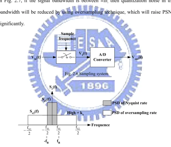
2.3.1 Oversampling Technique
First, we made the assumption that quantization noise is a uniform distribution in sampling spectrum so its mean is zero and is a white noise [34]. The system in Fig. 2.6 just has oversampling function and does not have noise shaping effect. If a A/D converter is sampled in Nyquist rate, then the quantization noise is uniform distributed between ±fB ; if it is sampled by oversampling technique, then quantization
noise is uniform distributed between± fS2/2s, which is much larger than fB. As shown
in Fig. 2.7, if the signal bandwidth is between ±fB, then quantization noise in this
bandwidth will be reduced by using oversampling technique, which will raise PSNR significantly.
Fig. 2.6 Sampling system
Frequence Se(f) 2 fS1 2 fS1 − 2 fS2 2 fS2 − fB -fB PSD of Nyquist rate PSD of oversampling rate High = kx Se1(f) Se2(f)
Fig. 2.7 Noise distribution after sampling
In the condition of oversampling, the PSD (Power Spectrum Density) of quantization noise is as Se2(f) in Fig. 2.7 and can be represented as:
kx2 = s 2 LSB f 12 V ⋅ = Se2 2(f) (2.7)
From (2.7) we can estimate the quantization noise in 2fB after oversampling PQ =
∫
− ⋅ B B f f 2 x df k = OSR 2 12 FS 12 V f f 2 B 2 2 2 LSB s B ⋅ ⋅ = ⋅ (2.8)In (2.8), we define a parameter OSR (Oversampling Ratio) as OSR = B s f 2 f (2.9) Finally, we can get PSNR from (2.5) and (2.8)
PSNR = 10 log( Q signal P P )= 6.02B + 1.76 + 10 log(OSR) (2.10)
From (2.10), we can find that doubling OSR will increase 3dB in PSNR, which is about 0.5 bit increase in resolution. Although oversampling can reduce quantization noise, it is difficult to reach high SNR when using a low bit quantizer. For example, if we need a 16bit A/D converter, then SNR must be equal to 98dB, if the signal bandwidth is 20KHz, then the sampling rate must equal to 2 × 109 × 20KHz, it is impossible to implement. Because at such high frequency, quantization noise is no longer a white noise, it is correlated with input signal. So there is not only oversampling technique, we must add noise shaping technique also, if we want to achieve high resolution.
2.3.2 Noise Shaping
We can model a general ΣΔ modulator and its linear model as shown in Fig. 2.8.
H(z) Quantizer y(n) x(n) u(n) (a)
(b)
Fig. 2.8 (a) General ΣΔ modulator (b) Linear model with quantization noise
From Fig. 2.8(a), we can derive output Y(z) as (2.11) Y(z) = ) z ( H 1 ) z ( H + X(z) + 1 H(z) 1 + E(z) (2.11) and define Signal Transfer Function STF and Noise transfer function NTF as
STF (z)= ) z ( H 1 ) z ( H ) z ( X ) z ( Y + = (2.12) NTF (z)= ) z ( H 1 1 ) z ( E ) z ( Y + = (2.13) where H(z) is the transfer function of a discrete time filter. There have two important meanings in (2.12), (2.13). If we want to obtain highest SNR, STF must be equal to 1,
that means the input signal can transfer to output without attenuating; and NTF (z)
must be equal to 0, because the quantization noise will not affect output SNR.
In order to make NTF (z) be a high pass filter, so at DC(z = 1), NTF must be 0, and z
= 1 is a pole of H(z), so the transfer function H(z) of the discrete filter is as H(z) = 1 Z 1 − = 1 1 Z 1 Z − − − (2.14) Substitute (2.14) into (2.12) and (2.13), we can get
STF (z) = z 1 (2.15) NTF (z) = z 1 1− (2.16) And we substitute z with fs
f 2 j
e
π
, then we can plot STF(f)2 and NTF(f) 2 in frequency domain, as Fig. 2.9. We can find NTF(f) 2 also increases with frequency, and
) f (
STF 2 is always equal to 1, if we choose signal bandwidth in low frequency, then we can get highest signal power and lowest noise power, from this figure we see that quantization noise is moved to higher frequency significantly, this is the noise shaping effect. 2 TF(f) N 2 TF(f) S
Fig. 2.9 Noise shaping
After noise shaping, we can filter out the noise in high frequency by using digital filter, and we will illustrate its architecture more detail in the next chapter.
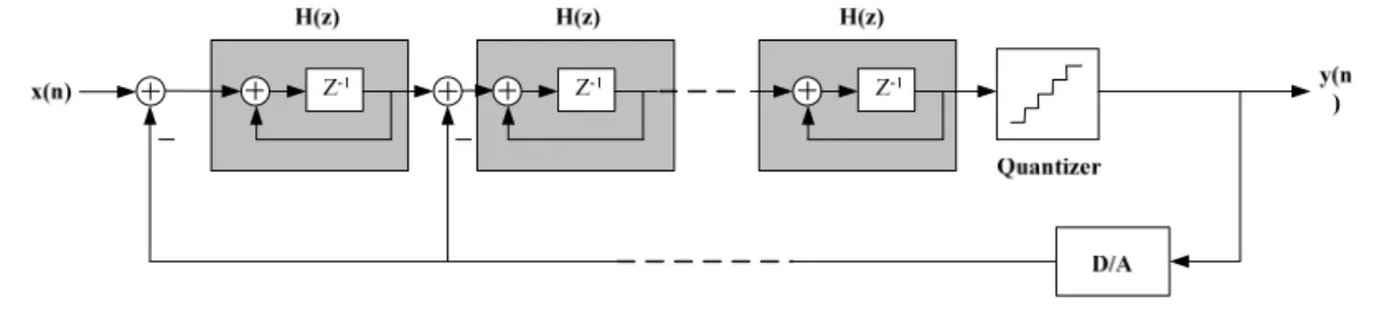
2.4 Architectures of Sigma-Delta Modulator
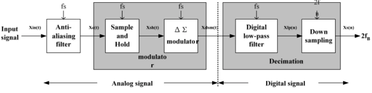
Before we introduce various architectures of ΣΔ modulators, we must to realize the basic architecture of a general ΣΔ A/D converter. Fig. 2.10 is a complete block diagram of a A/D converter [32], and we can divide it into two different parts. First part is the modulator. The main function of this part is doing oversampling and noise shaping to the input analog signal. Second part is the decimation filter. The main function of this part is to remove noise in high frequency and down sampling the sampling frequency to base band frequency.
ΣΔ ΣΔ
Fig. 2.10 Block diagram of ΣΔ A/D converter
First, the input signal Xin(t) pass an Anti-aliasing filter, the 3dB frequency of this filter is about few times of Nyquist frequency, so signal and noise out of Nyquist frequency is filtered roughly, and this signal goes into the ΣΔ modulator after goes through a S/H circuit. However, in the circuits implement situation, the sample and hold function is included in the circuits of ΣΔ modulator, so the signal Xc(t) will pass this modulator and produces a high speed data code Xdsm(n), because of noise shaping, the quantization noise will appear in high frequency. Finally, we must filter the noise in high frequency and reduce the sampling frequency to Nyquist frequency by a decimator, and passes the digital signal to the output [32].
In this chapter, we will focus on the architectures of ΣΔ modulator, because that the noise model and optimal method is focus on this part, we must understand the theorem, benefits and drawbacks of each kinds of ΣΔ modulators. In addition, the implement of decimator is very typical [35, 36]. In today’s technology, DSP processors are also used to replace decimators, so we will introduce this part roughly.
2.4.1 First-Order Sigma-Delta Modulator
We recall that H(z) in (2.14) is 1 1 Z 1 Z − −
− , substitute it into Fig. 2.8, then we can get a
first-order modulator; Analyze transfer function H(z) from time-domain, it
indicates that output signal m(t) is obtained by adding the delayed input signal n(t-1) ΣΔ
and the delayed output signal m(t-1), so we can express a complete first-order modulator as Fig. 3.2.
ΣΔ
Fig. 2.11 First-order ΣΔ modulator
H(z) in Fig. 2.11 is indicated the effects of delay and accumulation, this is
equivalent with an integrator in circuit design, so the three circuits components of modulator are integrator, quantizer and DAC in the feedback path. A first order ΣΔ modulator’s output can represent as
ΣΔ
Y(z) = z-1X(z) + (1-z-1)E(z) (2.17) From (2.17) we can find the signal transfer function is as a delay function, and noise transfer function is as a high pass filter, moves the noise to high frequency. In order to derive PSNR of first order modulator, we must get the magnitude of NTF(z) and
STF(z) in the frequency domain, so we substitute z with , and get
ΣΔ s f / f 2 j e π⋅ STF(f) and (f) NTF respectively as: 1 j2πf/fs TF(f) z e S = − = − ⋅ = 1 (2.18) NTF(f) = 1-e−j2π⋅f/fs= j f/fs s e j 2 ) f f sin(π × × −π⋅ ⇒ TF( ) 2 sin( ) f f N = ⋅ π (2.19)
So the quantization noise in base band ±fB can obtain by (2.7) and (2.19) PQ = df f f sin 2 f 12 V df ) f ( N ) f ( S 2 f f s s 2 LSB 2 TF f f 2 e B B B B ⋅ ⎥ ⎦ ⎤ ⎢ ⎣ ⎡ ⎟⎟ ⎠ ⎞ ⎜⎜ ⎝ ⎛ ⋅ ⋅ = ⋅
∫
∫
− − π (2.20) Because that fB is much lower than fs, so sin(π f/fs) is approximate equal to (π f/fs),and PQ is as PQ = 3 2 2 LSB ) OSR 1 ( 36 V ⋅ π = 2B 3 2 2 OSR 2 36 FS ⋅ ⋅ ⋅π (2.21) From (2.5) and (2.21), if we have the maximum signal power, then PSNR is as (3.6) PSNR = 10 log( Q signal P P ) = 10 log( 22B 2 3 ) + 10 log[ 3 2 (OSR) 3 π ] = 6.02B + 1.76-5.17 + 30 log(OSR) (2.22) (&)From (2.22), we find that each octave of OSR, PSNR will increase 9dB, increase 1.5 bit in resolution. Compare (2.22) with (2.10) that only has oversampling effect; we can find that 1st order noise shaping increases the performance of ΣΔ modulator.
2.4.2 Single-Loop Second-Order Sigma-Delta Modulator
When the discrete time filter in Fig. 2.8 is replaced by two cascade integrator, then it is a second order ΣΔ modulator, output of the first integrator is only connecting with the input of the second integrator, it is shown in Fig. 2.12
Then the output of it can easily be derived as
Y(z) = z-2X(z) + (1-z-1)2E(z) (2.23) where STF and NTF is as
STF(z) = z-2 (2.24)
NTF(z) = (1- z-1)2 (2.25)
Using the same method in (2.19) (2.20), we can obtain
STF(f) =1 (2.26) 2 s TF f f sin 2 ) f ( N ⎥ ⎦ ⎤ ⎢ ⎣ ⎡ ⎟⎟ ⎠ ⎞ ⎜⎜ ⎝ ⎛ ⋅ = π (2.27) PQ = 5 4 2 LSB OSR 60 V ⋅ ⋅π = 2B 2 4 5 OSR 60 2 FS ⋅ ⋅ ⋅π (2.28) So finally, PSNR of the second order ΣΔ modulator is as
PSNR = 10 log( Q signal P P ) = 10 log( 22B 2 3 ) + 10 log[ 5 4 (OSR) 5 π ] = 6.02B + 1.76-12.9 + 50 log(OSR) (2.29) In the single loop second order architecture, each octave of OSR can increase PSNR by 15 dB, it is equivalent to 2.5 bit in resolution. If we compare (2.29), (2.27) with
) f (
NTF =1 that without noise shaping, as Fig. 2.13, we can find that in our needed signal bandwidth, the quantization noise is highest when NTF(f) =1, and that with second order noise shaping is smallest among this figure [32].
TF N No noise shaping First-order Second-order f fS fB 2 fS
Fig. 2.13 Comparison of noise shaping techniques
2.4.3 Single-Loop High Order Sigma-Delta Modulator
Fig. 2.14 is a single loop high order ΣΔ modulator, from the derivation in Section 2.4.1 and Section 2.4.2, we can get the quantization noise PQ in signal bandwidth is as
PQ = 2L 1 L 2 2 LSB ) OSR 1 ( 1 L 2 12 V ⋅ + + ⋅ π ,L:order (2.30) and its PSNR is PSNR = 6.02B+1.76-10 log( 1 L 2 L 2 + π )+(20L+10) log(OSR) (2.31)
In the application of high order ΣΔ modulator, (6L+3)dB increases in SNR when
OSR is octave, so PSNR can be raised by increasing the order of the system, especially at large oversampling ratio. But sometimes in high order architecture, the performance will be worsen than result predicted by (2.29), because of the stability problem, it will make less effective noise shaping function, so the quantization noise will not be suppressed completely.
Fig 2.14 Single-loop high order ΣΔ modulator
2.4.4 Interpolative Sigma-Delta Modulator
Interpolative is a kind of high order ΣΔ modulator, it changes connection of some stages, adds some feed forward paths and feedback paths in order to suppose more aggressive noise shaping effect, Fig. 2.15 is a four-order interpolative architecture
modulator [37]. ΣΔ 1 1 z 1 z − − − 1 1 z 1 z − − − 1 1 z 1 z − − − 1 1 z 1 z − − − b DAC y(n) x(n) Quantizer
Fig. 2.15 Four-order interpolative architecture
This architecture also has stability problem, when the order L increases, each integrator produces one pole, and when the order is higher, poles of this system will also increase, and it will cause unstable situation, so the range of integrator gain will be limited; if the range of integrator gain is small, oscillation will appear in the circuits. Another is the considerations of clock control, when we use SC (switched-capacitor) to implement the integrator, each integrator needs two clocks to control its operation, and we will need more clock to control the integrator when the order of system increases, it will produce more problems.
2.4.5 MASH Architecture
MASH (Multi-stage noise shaping) architecture is also called cascade architecture, which is a method that cascades several low order loops modulator in order to get high order noise shaping effect. The fundamental ideal of MASH is delivering quantization noise of front stage to input of next stage, and combining the digital outputs of all the stages with proper transfer function in digital domain, only the quantization noise of last stage will appear at the output, and the orders of NTF is the
same with total orders in the cascade ΣΔ modulator. Fig 2.16 is a three-order
cascade modulator, its is the combination of a second-order and first-order modulator, so also called 2-1 cascade architecture.
ΣΔ ΣΔ 1 − Z 1 − Z Z−1
Fig. 2.16 2-1 architecture MASH ΣΔ modulator
From Fig. 3.7, we can derive the first stage output Y1(z) can be represented as
Y1(z) = z-2X1(z) + (1-z-1)2E1(z) (2.32)
Output of second stage Y2(z) is as
Y2(z) = z-1X2(z) + (1-z-1)E2(z) (2.33)
Y(z) = H1(z)Y1(z) + H2(z)Y2(z) (2.34)
and we can say that second stage input X2(z) is almost the same with E1(z), in order to
eliminate first stage quantization noise E1(z), from (2.32) ~ (2.34), we can define the
error cancellation functions H1(z) and H2(z) as
H1(z) = z-1 (2.35)
H2(z) = (1-z-1)2 (2.36)
From (2.32)~(2.36), E1(z) can be eliminated, and second stage quantization noise E2(z)
is shaped by third-order noise shaping function, and the MASH output Y(z) is as Y(z) = z-3X1(z) + (1-z-1)3E2(z) (2.37)
The most significant advantage of this architecture is that stability is not an issue, because it is composed by several low-order systems, and the quantization noise will not be amplified stage by stage, so its stability is good. Most important, the noise shaping function is equivalent as high order ΣΔ modulator, so it is popular in recent publications [38, 39]. However, there also have some drawbacks of this topology; it is sensitive to the circuits' imperfections, such as finite DC gain of OTA, variance of integrator gain due to capacitor mismatch and non-zero switch resistance. These are
all practical considerations when we design a MASH architecture modulator
[40].
ΣΔ
2.4.6 Multi-bit Quantizer Sigma-Delta Modulator
The demands of high resolution and high bandwidth ADC are more and more in recent years. In a high signal bandwidth, OSR of ΣΔ ADC can’t be too high, and the peak SNR of a modulator with such limited OSR can’t satisfy of high resolution applications, if we use higher order architecture, then the performance will degrade due to instability. So the most general method to increase performance is to use
distance between quantizer level VLSB in (2.4) is much smaller due to increasing of B,
and according to (2.3), the power of quantization noise is attenuated. Fig. 2.17 is the results of theoretical peak SNR of ΣΔ modulator versus oversampling ratio, with different order and quantizer bits, it is noted that peak SNR of the same OSR is increase 6 dB with each additional bit number in quantizer, and at low OSR, low order higher bit number architecture has equivalent performance as high order architecture. This result is usable for high bandwidth applications, and the power consumption of digital circuit in ΣΔ modulator is reduced due to lower sampling rate [41].
160 0 50 100 150 200 250 300 20 40 60 80 100 120 140 O2B1 O2B2 O2B3 O3B1 OSR S NR
Fig. 2.17 SNR vs. OSR with different quantizer bit number
Because of using multi-bit quantizer, so we also need to use multi-bit DAC(Digital-to Analog Converter) to transfer the digital output to analog signal, and feed it back to integrator. The most significant disadvantage is the non-linearities introduced by multi-bit DAC can degrade the performance of ΣΔ converter, like Fig. 2.18. It is a
linear model of multi-bit modulator, where E(Q) and E(D) represent the
quantization noise and feedback DAC noise respectively. The values of these capacitor elements in DAC will not equal to ideal values that we need, it is due to
process variation, typical value of mismatch in modern CMOS technology is about 0.05% ~ 0.5%. In recent years, so many researches are make efforts on reduce DAC noise due to mismatch, such as trimming [42], Dynamic element matching(DEM)[33, 43], although trimming is effective, but it has a expensive production step. So, DEM becomes more and more popular because of its efficiency and cheaper cost.
Fig. 2.18 Multi-bit architecture
2.4.7 Multi-bit Sigma-Delta Modulator use DEM Technique
Dynamic element matching is a different approach to decrease the DAC noise, it is used to improve the linearity of pure DACs [44], but now it is most used in inner DAC of multi-bit ΣΔ modulator. A DAC with DEM technique is illustrated in Fig. 2.19, bits thermometer code is put into the element selection logic block, and the function of element selection logic is try to select DAC elements in such way let the errors introduced by DAC average to zero for several operation periods. Because the DEM block is located in feedback loop, so its delay must be very small prevent to degrade the performance of converter, therefore the algorithm used in the DEM block must be simple. There are several techniques of DEM, such as Randomization
B
2
[45], Clocked Averaging (CLA) [47], Individual Level Averaging (ILA) [46], Data Weighted Averaging (DWA) [47], Randomization is the first approach to use DEM
technique in ADC, and DWA offers a good performance to reduce DAC error,
in this section, an overview introduction of these two algorithms will be presented, and the operation principle of them will be explained.
ΣΔ 1 2B− 1 2 B 2 B 2
Fig. 2.19 A B-bit DAC with DEM technique
2.4.8 Decimator
In A/D converter, digital decimator is used to process digital signal of the quantizer output, the high speed data word after oversampling modulation can’t be used directly. Because there have original signal and quantization noise among it, so the main function of decimator is to convert the oversampled B-bit output words of the quantizer at a sampling rate of fs to N-bit words at Nyquist rate of input, and removes the noise out of signal band. In order to prevent the noise introduced by other frequency, the decimator filter must have very flat signal pass-band, and sharp transition region and enough signal attenuation in stop band. Two-stage decimator is used in a general situation, because that single stage decimator is difficult to convert sampling rate to Nyquist rate in 1 time and without degrading SNR. In the first stage, we can down-sample the sample frequency to 2~4 times of Nyquist frequency, and in the second stage, we can use IIR or FIR filter that have high linearity [42]. For a large
OSR, multi-stage decimator is used.
2.4.9 Performance Metrics for a
ΣΔModulator
In order to understand the performance merits used to specify the behavior of modulator, several specifications concerning the performance are discussed [30].
ΣΔ
․Signal to Noise Ratio: The SNR of a data converter is the ratio of the signal power to the noise power, measured at the output of the converter for a certain input amplitude. The maximum SNR that a converter can achieve is called the peak SNR.
․Signal to Noise and Distortion Ratio: The SNDR of a converter is the ratio of the signal power to the power of the noise and the distortion components, measured at the output of the converter for a certain input amplitude. The maximum SNDR that a converter can achieve is called the peak SNDR.
․Dynamic Range at the input: The DRi is the ratio between the power of the
largest input signal that can be applied without significantly degrading the performance of the converter, and the power of the smallest detectable input signal. The level of significantly degrading the performance is defined as the point where the SNDR is 6 dB bellow the peak SNDR. The smallest detectable input signal is determined by the noise floor of the converter.
․Dynamic Range at the output: The dynamic range can also be considered at the output of the converter. The ratio between maximum and minimum output power is the dynamic range at the output DRo, which is exactly equal to peak SNR.
․Effective Number of Bits: ENOB gives an indication of how many bits would be required in an ideal quantizer to get the same performance as the converter. This numbers also includes the distortion components and can be calculated from (2.6)
02 . 6 76 . 1 ENOB= SNR− (2.38)
․Overload Level: OL is defined as the relative input amplitude where the SNDR is decreased by 6dB compared to peak SNDR
Typically, these specifications are reported using plots like Fig. 2.17. This figure
shows the SNR and SNDR of the ΣΔ converter versus the amplitude of the
sinusoidal wave applied to the input of the converter. For small input levels, the distortion components are submerged in the noise floor of the converter. Consequently, the SNDR and SNR curves coincide for small input levels. When the input level increases, the distortion components start to degrade the modulator performance. Therefore, the SNDR will be smaller than the SNR for large input signals. Note that these specifications are dependent on the frequency of the input signal and the clock frequency of the converter. Fig. 2.20 also shows that SNDR curves drop very fast once the overload point is achieved. This is due to the overloading effect of the quantizer which results in instabilities.
3.OTA Non-Linear Gain Curve
Existing OTA nonlinear gain distortion models in Sigma-Delta Modulator consume much time to obtain. Usually OTA nonlinear gain curve parameters are identified directly from transistor-level designs. Although the nonlinear gain curve parameters obtained this way are more accurate, it is hard to generalize from one design case to another. In addition, there are two more problems. First, due to that they consume much time to obtain OTA nonlinear gain curve parameters, it is not practical to achieve desired results in a recursive way. Second, it is hard to know how nonlinear gain curve parameters are affected by sigma-delta modulator circuit
parameters, e.g., OTA dc gain Ao, OTA output swing voltage VOS, etc.
Two of major op-amp architectures are popular with low-power IC design. First architecture is the two-stage op amp. It consists of a cascade of V→I and I→V stages. This two-stage op amp is so widely used that we call it the classical two-stage op amp. Second architecture major architecture is commonly called the folded-cascade op amp. Architecture of classical two-stage architecture is widely used in SDM design. It comprises differential amplifier in first voltage stage and output amplifiers in second voltage stage, see as Fig. 3.1.
Fig 3.1 Two-Stage OTA architecture
of classical two-stage op-amp with class-A stage. It’s typical op-amp’s configuration schematic see as Fig.3.2.
In the practical op amp circuit, the nonlinearity of the gain is manifested by its dependency on amplifier output voltage . Fig. 3.3 shows a typical relationship
between DC gain and , in which the maximum DC gain appears at
O
V
O
V AO
Fig. 3.2. A typical op-amp’s configuration schematic considering nonlinear DC gain
Fig. 3.3. A typical relationship between DC gain and Vo
center of scale and decreases as the magnitude of output voltage increases. This nonlinear gain introduces distortion in the sigma-delta modulator output spectrum. After some HSPICE simulation based on TSMC 0.18μm, the results reveal that VGSQ
A0=570,VOS=1V
A0=321,VOS =1V
Fig.3.4. Two nonlinear gain curves with identical VOS but different A0
A0=331,VOS=1.6V A0=321,VOS =1V
Fig.3.5. Two nonlinear gain curves with similar but different A0 VOS
the nonlinear curves. In order to make designers easier to use, it is must to replace
GSQ
V by a more general parameter in circuit. By the basal op amp circuit concept, we
can know the range of maximum output swing ( )VOS and VGSQ are germane relation
with each other. Thus, in dealing with OTA distortions, we are basically faced with a family of nonlinearities.
About the distortion due to a particular nonlinear curve approximated by the polynomial:
) 1 ( ) ( 4 4 3 3 2 2 1 0 + + + + +L = o o o o o VV A qV qV qV qV A (3.1)
Because the nonlinear curve is even function, it can be simplified by:
) 1 ( ) ( 6 6 4 4 2 2 0 + + + +L = o o o o VV A qV qV qV A (3.2)
Where is finite DC gain of OTA, and is the maximum finite DC gain
when is in the neighborhood of 0V.
) (VO Av O V O A
Although some expressions for harmonic distortions are derived in [30] and [48], these results are not completed. They just offer an incomplete model, due to they model must use transistor level to assist their distortion model complete. In this subsection, we will drive a complete OTA gain distortion model for 0.18μm process. There are two steps. In the first step, we try to model the family of nonlinear curves. Next, based on this nonlinear curve model, we derive the distortion model. The behavior simulation model offered by [49] is applied to verify this model.
For the first step, our HSPICE simulation based on TSMC 0.18μm process model reveals that, in addition to output voltage Vo, both the VGS of output stage
transistors and the maximum DC gain can affect the shape of the nonlinear curves. Thus, in dealing with OTA distortions, we are basically faced with a family of nonlinearities. Since VGSQ is inversely proportional to the range of maximum output
swing , we identify , and V as the three parameters that can affect OTA
DC gain . We simulated on a classical two-stage operation amplifier shown in Fig. 3.6 to produce two specific cases shown in Fig. 3.4 and Fig. 3.5. Figure 3.5 shows how variation in can affect the curve shape. Figure 3.5 demonstrate the case when
O A OS OS V A O V AO V O A
variation is mainly in . In order to model the nonlinear DC gain , we tried
various combination of and to the curve shape. In order to model the
nonlinear DC gain , we tried various combination of and to create a set of representative curves for the family of nonlinear DC gain curves. Then, after intensive
OS V A V A O VOS V A AO VOS
Fig. 3.6. A classical two-stage operation amplifier
trials and errors, we come up with the following function to fit the nonlinear curves.
( , , ) {1 0.5 [ (0.443 ) ( 0.443 1.2 ) 2]} 03 . 0 0 2 . 1 03 . 0 0 0 0 = ⋅ − ⋅ ⋅ + − ⋅ o − os o os o OS V V V A EXP V V A EXP A V V A A (3.3)
After performing Taylor’s series expansion on (14) over , the model we arrive at is of the form o V ( ) (1 4) (3.4) 4 2 2 0 o o o VV A qV qV A = + +
where q2and
q
4 in (5.17) are2 2 . 1 03 . 0 0 2 (0.443 ) 2 1 OS V A q =− ⋅ ⋅ (3.5) 4 2 . 1 03 . 0 0 4 (0.443 ) 24 1 OS V A q =− ⋅ ⋅ (3.6)
discriminate the circuit parameter effect upon OTA gain distortion clearly.
In the past, it is hard to decide DC gain to achieve high-linear. Because modern ICs are asked for low power consumption, DC gain isn’t the bigger the better. Designers can plan a recursive way with our approach. For example, if designer expect the HD3 is -110 dB. Users can easily know that q2 is needed -0.170521 and q4 is needed -0.004846 and designers can decide important parameters (e.g., OTA dc gain, OTA output swing voltage etc) in design flow.
At last, we simulate a practical two op amps to verify our non-linear gain curve model. First, we simulate op-amp with class-B stage. It’s parameter is
Ao=68dB,Vos=±1.5V. See Fig.3.8, when Vo swing in (+0.87V~-0.87V), the simulation result of nonlinear curve function is close to the practical one. The 2nd order nonlinear coefficient of the nonlinear curve function q2= - 0.0593 is close to that of the practical case q2= -0.0561, but the 4th order nonlinear coefficient of the nonlinear curve function q4=-0.000586 is much larger than that of practical case q4= -0.00873. -2 -1.5 -1 -0.5 0 0.5 1 1.5 2 1800 1900 2000 2100 2200 2300 2400 2500 Vo(V) D iff er en tia l G ain
Fig.3.8. Comparison between simulation of nonlinear curve function and practical design
Second, we simulate op-amp with class-A stage. It’s parameter is
Ao=50dB,Vos=±1.6V. See Fig.3.9, when Vo swing in (+1V~-1V), the simulation result of nonlinear curve function is close to the practical one. The 2nd order
nonlinear coefficient of the nonlinear curve function is close to that of the practical case , but the 4th order nonlinear coefficient of the nonlinear curve
function is much larger than that of practical case since is
very sensitive and difficult to be estimated, it causes that the 5th harmonic distortion estimation is not accurate,
1387 . 0 2=− q q 1106 . 0 2=− q 0032 . 0 4=− 4 4 q =−0.0451 q
Fig.3.9. Comparison between simulation of nonlinear curve function and practical design
Because our nonlinear gain model are build with class-A in second stage, The simulate with class-A is more accurate than class-B. No matter what Architecture is, q2 is still enough to obtain a accurate HD3. Because it’s the most important factor for HD3.
4.
Distortion Due to the Non-Linear Gain
of the Operational Amplifier
An ideal OTA with infinite gain doesn’t introduce any noise or distortion.
Practical OTAs not only have the characteristics of finite DC gain, but also the gain is nonlinear. In chapter four, we analyze the op amps non-linear gain phenomenon. We also obtain the non-linear gain curve model aimed the classical two-stage. So the next work is to obtain the expressions to estimate harmonic distortion introduced by integrator with our non-linear gain curve model.
(a) Sampling phase (b) integration phase Fig. 4.1. Switch-capacitor integrator with finite-gain amplifier
See Fig 4.1(a) and 4.1(b), First, in order to obtain more accurate distortion model we must analyze the charge transfer in integrator. By Fig. 4.1 we can obtain the charge transfer in integrator is
( − +)⋅ 1 =( O+− O−)−( a+− a−) I a S SV V C V V V V C (4.1) Arrange function
CI⋅VO−Va −CS⋅Va =CI⋅VO−Va +CS⋅V
(4.2) − − + + + ) ( ) (
Up to the present, we obtain three important functions in nonlinear gain analyze. First, the nonlinear gain curve model. Second, the charge transfer functions in integrator. Third, the behaving characteristic functions of op amp. See below
( ) (1 4) (4.3) 4 2 2Vo qVo q Ao Vo AV = + + CI⋅(Vo+−Va+)−CS⋅Va+=CI⋅(Vo−−Va−)+CS⋅V (4.4)
Vo±=−A Vo± ⋅Va±
(4.5) V( )
Substituting (4.3) and (4.4) into (4.5), one obtains the following expression
] ) ( ) ( ) 1 [( ) 1 1 ( ) / 1 1 ( 3 3 0 2 0 0 − + − +− + ⋅ − + ⋅ − ⋅ + + = ⋅ o o I S a o I S s I S V V C C A q V A V A C C V C C [(1 ) ( )5 ( )5] 0 4 + ⋅ + − − − o o I S V V C C A q (4.6)
In order to simplify (4.6), it is assumed in [30] that (1 1 / ) 1 0 ≅ + + A C CS I , (1 1) 1 0 ≅ + A , and the
final expression can be derived as
− +−Vo Vo 2 2 1 3 4 4 2 2 2 [( ) ( )] [( ) ( )( ) ( )( ) 1 { − ⋅ + + + −+ − − + + + − + + − ⋅ ≅ Vo Vo Vo Vo Vo Ao q Vo Vo Vo Vo Ao q C C I S S V Vo Vo Vo + ⋅ +( +)1( −)3 ( −)4}−1 (4.7)
Using Taylor’s series expansion on over Ao
− +−Vo Vo 1 3 4 4 2 2 2 (( ) ( )( ) ( ) ) (( ) ( )( ) [ 1 1 {+ ⋅ ⋅ + + + − + − + ⋅ + + + − ⋅ = q Vo Vo Vo Vo q Vo Vo Vo Ao C C I S )] ) ( ) ( ) ( ) ( ) ( + 2 − 2+ +1 − 3+ − 4 +Vo Vo Vo Vo Vo 1 3 4 4 2 2 2 2 [ (( ) ( )( ) ( ) ) (( ) ( )( ) 1 ⋅− ⋅ + + + − + − − ⋅ + + + − + q Vo Vo Vo Vo q Vo Vo Vo Ao S V Ao Vo Vo Vo Vo Vo + + + ⋅ + + − + − − ∞} 1 )] ) ( ) ( ) ( ) ( ) ( 2 2 1 3 4 L
(4.8)
1 3 4 4 2 2 2 (( ) ( )( ) ( )) (( ) ( )( ) [ 1 { ⋅ ⋅ + + + − + − + ⋅ + + + − ⋅ q Vo Vo Vo Vo q Vo Vo Vo Ao C C I S ) ) ( ) )( ( ) (( [ 1 )] ) ( ) ( ) ( ) ( ) ( 2 2 2 2 4 3 1 2 2 − + − − + + − − + + + + ⋅− ⋅ + + + q Vo Vo Vo Vo Ao Vo Vo Vo Vo Vo
VS Ao Vo Vo Vo Vo Vo Vo Vo Vo q ⋅ + + + + + ⋅ − (( +)4 ( +)3( −)1 ( +)2( −)2 ( +)1( −)3 ( −)4)] 1∞} 4 L
(4.9)
In order to build a mathematical expression related to input signal magnitude for estimating the distortion caused by nonlinear DC gain, and must be expressed as functions of . In single-loop second-order sigma-delta modulator, when a signal apply to modulator input and quantization noise is not considered, can be represented as ± O V VS in A ) (wnT Sin VS ) ) 2 ( sin( ) sin( ) (nT A wnT A wn T VS in in S = − − ( ) ( )⎥ ⎦ ⎤ ⎢ ⎣ ⎡ − ⋅ − ⋅ = wnT OSR wnT OSR Ain ) cos 2 sin( sin )) 2 cos( 1 ( π π (4.10)
The output signal of the first integrator can be represented input signal See Fig. 4.2 Fig. 4.2 Integrator As t = nT, in sample phase ) ( QC1=C1⋅VinnT (4.11) ⎥ ⎦ ⎤ ⎢ ⎣ ⎡ ⋅ ⎟ ⎠ ⎞ ⎜ ⎝ ⎛ − ⋅ =C V n T QC O 2 1 2 2 (4.12) As t = (n+1/2)T, in integration phase
) ( 2 1 2 1 1 2 2V n T CV n T CV nT C O O ⎥− in ⎦ ⎤ ⎢ ⎣ ⎡ ⋅ ⎟ ⎠ ⎞ ⎜ ⎝ ⎛ − = ⎥ ⎦ ⎤ ⎢ ⎣ ⎡ ⋅ ⎟ ⎠ ⎞ ⎜ ⎝ ⎛ + ) ( ) ( ) ( 2 1 1 2 2 1 2V z z CV z z CV z C O ⋅ = O ⋅ − in ⇒ − 1 2 / 1 2 1 2 / 1 1 ) ( ) ( ) ( − − − ⋅ − = = ∴ z z C C z V z V z H in O (4.13)
So, we can obtain
) ( 2 / 1 jw H V VO = S⋅ ±
{
V H1/2(jw)}
{ V H1/2(jw)} VO = S ⋅ ⋅ ∠ S⋅∠ ± ⎟ ⎠ ⎞ ⎜ ⎝ ⎛ ± ⋅ ⋅ ⋅ − = Cos wn T wT Sin A C C in ) 2 1 ( 2 2 2 1 (4.14)We can clean find that output voltage and input voltage are integral relation. Then we simplify function
⎟ ⎠ ⎞ ⎜ ⎝ ⎛ ± ⋅ ⋅ ⋅ − = ± Cos wn T wT Sin A C C V in O ) 2 1 ( 2 2 2 1 ⎟ ⎠ ⎞ ⎜ ⎝ ⎛ ⋅ ⋅ ⋅ ⋅ ⋅ ⋅ ⋅ − = ) 2 ( ) ( ) 2 ( ) ( 2 2 2 1 OSR Sin wnT Sin OSR Cos wnT Cos wT Sin A C C in π m π (4.15)
Then (4.10) (4.15) replace Vo and Vs into the nonlinear tern
) ( ) 5708 . 1 ( 75 . 0 { 1 2 2 2 2 2
1 A q Cot OSR Cos nTw
a A C C in O I S⋅ ⋅ ⋅ ⋅ ⋅ ⋅ ) ( 25 . 0 ) ( ) 5708 . 1 ( 3125 . 0 2 2 2 2 1 4 4 4 4 4 1 Cos nTw a A q Sin nTw OSR Cot q A a ⋅ in⋅ ⋅ ⋅ + ⋅ ⋅ in⋅ ⋅ ⋅ + S in
in Cos nTw Sin nTw a A q Sin nTw V
OSR Cot q A a ⋅ ⋅ ⋅ ⋅ ⋅ + ⋅ ⋅ ⋅ ⋅ ⋅ ⋅ +0.625 (1.5708) ( ) ( ) 0.0625 4( )} 4 4 4 1 2 2 2 4 4 4 1 (4.16) Coordination function
ASin_3×Sin(3nTw)+ACos_3×Cos(3nTw)+ASin_5×Sin(5nTw)+ACos_5×Cos(5nTw) (4.17) Where
⎪ ⎪ ⎪ ⎩ ⎪⎪ ⎪ ⎨ ⎧ ⋅ ⋅ ⎟⎟ ⎠ ⎞ ⎜⎜ ⎝ ⎛ ⋅ ⎟ ⎠ ⎞ ⎜ ⎝ ⎛ ⋅ − ⋅ ⋅ = 16 1 ) 5708 . 1 ( 3 [ 1 A 2 3 2 2 3 _ q A C C OSR Cot A C C I in S O I S Sin ⎥ ⎦ ⎤ ⎢ ⎣ ⎡ − ⋅ ⎪ ⎪ ⎪ ⎭ ⎪⎪ ⎪ ⎬ ⎫ ⋅ ⋅ ⎟⎟ ⎠ ⎞ ⎜⎜ ⎝ ⎛ ⋅ ⎟ ⎠ ⎞ ⎜ ⎝ ⎛ ⋅ + ⋅ − + ] 1 ( 2 ) 16 3125 . 0 ) 5708 . 1 ( 625 . 0 ) 5708 . 1 ( 9375 . 0 4 5 4 2 4 OSR Cos q A C C OSR Cot OSR Cot in I S π (4.18) ⎪ ⎪ ⎪ ⎩ ⎪⎪ ⎪ ⎨ ⎧ ⋅ ⋅ ⎟⎟ ⎠ ⎞ ⎜⎜ ⎝ ⎛ ⋅ ⎟ ⎠ ⎞ ⎜ ⎝ ⎛ ⋅ − ⋅ ⋅ = 16 1 ) 5708 . 1 ( 3 [ 1 A 2 3 2 2 3 _ q A C C OSR Cot A C C I in S O I S Cos ⎥ ⎦ ⎤ ⎢ ⎣ ⎡ ⋅ ⎪ ⎪ ⎪ ⎭ ⎪⎪ ⎪ ⎬ ⎫ ⋅ ⋅ ⎟⎟ ⎠ ⎞ ⎜⎜ ⎝ ⎛ ⋅ ⎟ ⎠ ⎞ ⎜ ⎝ ⎛ ⋅ ⋅ − ) 2 ( ] 16 1875 . 0 ) 5708 . 1 ( 625 . 0 -) 5708 . 1 ( 1.5625 -4 5 4 2 4 OSR Sin q A C C OSR Cot OSR Cot in I S π (4.19) ⎥ ⎦ ⎤ ⎢ ⎣ ⎡ − ⋅ ⋅ ⋅ ⎟⎟ ⎠ ⎞ ⎜⎜ ⎝ ⎛ ⋅ ⎟ ⎠ ⎞ ⎜ ⎝ ⎛ ⋅ − ⋅ + ⋅ ⋅ = ] 1 (2 ) 16 0625 . 0 ) 5708 . 1 ( 625 . 0 ) 5708 . 1 ( 3125 . 0 [ 1 A 4 5 4 2 4 5 _ OSR Cos q A C C OSR Cot OSR Cot A C C I in S O I S Sin π (4.20) ) 2 ( ] 16 0625 . 0 ] 5708 . 1 [ 625 . 0 ] 5708 . 1 [ 3125 . 0 [ 1 A 4 5 4 2 4 5 _ OSR Sin q A C C OSR Cot OSR Cot A C C I in S O I S Cos π ⋅ ⋅ ⋅ ⎟⎟ ⎠ ⎞ ⎜⎜ ⎝ ⎛ × ⎥ ⎦ ⎤ ⎢ ⎣ ⎡ × − + − ⋅ ⋅ = (4.21)
So the powers of the 3rd and 5th harmonic distortions are
2 ) ( log 10 ) ( 3 2 3 _ 2 3 _ Cos Sin NFDCG A A dB HD = + (4.22)
2 ) ( log 10 ) ( 5 2 5 _ 2 5 _ Cos Sin NFDCG A A dB HD = +
(4.23)
In (4.18)-(4.21) we can obtain the relationships between the each parameter and power of the harmonic distortions, which are listed in Table 4.1.
Table 4.1 the relationship between the each parameter and the harmonic distortions
I
C ↑ CS↑ Ain↑ A0↑ Vos↑ OSR↑
Distortion size
5.Behaving Model Simulation Results
We use a calculable behaving model to verify our nonlinear gain distortion model.[49]
The z-domain transfer function of a delayed integrator of Sigma-Delta Modulator is 1 1 1 ) ( − − ⋅ − ⋅ = z z g z H α (5.1)
Where g and α are the integrator gain and leakage.
For a Typical integrator, the precise transfer function is
I S O O typ C C Ks z A Ks z A Ks Ks z H = ⋅ ⎟⎟ ⎠ ⎞ ⎜⎜ ⎝ ⎛ − − ⋅ ⎟⎟ ⎠ ⎞ ⎜⎜ ⎝ ⎛ − + ⋅ = − − , 1 1 1 1 ) ( 1 1 1 1 1 − − ⋅ − ⋅ = z a z g typ typ (5.2)
The nonlinear curve is
(1 3 ) (5.3) 3 2 2 1 + + +L + =AO VO VO VO A α α α
Then substitute into g and α
⎜⎜ ⎝ ⎛ − + − − − = 1 (1 1 O( S S) in( S S) O typ V nT T KsV nT T A Ks α α
)
) ) ( ) ( 2 2 − + − +L −α VO nTS TS KsVin nTS TS ⎜⎜ ⎝ ⎛ − + − − + − = 1 1 (1 1 O( S S) in( S S) O typ A V nT T KsV nT T Ks Ks g α)
) ) ( ) ( 2 2 − + − +L −α VO nTS TS KsVinnTS TSFig. 5.1 an nonlinear op-amp model in simulink
Then, we take op amp model into the complete sigma delta modulator. See as Fig.5.2
Fig. 5.2 Non-ideal second-order SDM
Now, we can use the non-ideal OTA behaving model in sigma delta modulator to simulate the OTA nonlinear gain distortion.
See as Table.5.1, Table.5.2, Table.5.3, we can find our model simulation results are close to behaving model simulation results. At different op-amp specifications, HD3 in our model is always close to simulation results.
Table.5.2 Comparison of theoretic result and behavior simulation of Case B
6.Transistor Level Simulation Results
The proposed model serves as a powerful tool for analyzing nonlinear gain distortion for sigma delta modulator. In order to assess the accuracy of the proposed methodology at circuit-level, the circuit of Fig. 6.1 has been realized using classical two-stage architecture in Spice.
Because the magnitude of transfer function of first op amp in sigma delta modulator is one, all of its noise wouldn’t loss in SDM output. So we can just use an op amp to simulate gain distortion.
Fig.6.1. two-stage Op-Amp
The specifications op the op amp are DC-gain=69dB,Vos=±1.43V, a1=1. Its FFT print See as Fig.6.2. Note that the even order harmonic distortions are ideally zero due to the symmetry of fully differential OTA. The total harmonic distortion (THD) is mainly determined by the third harmonic distortion (HD3). By Fig.6.2 HD3 and HD5 is -52.1dB and -72.9dB respective, our model simulation is that HD3 and HD5 is -47.0227dB and -63.0224dB respective. We can find that our HD3 is close to Spice simulation, it’s different about 5dB. But the q4 of our model isn’t accurate enough, our
neglect always in common sigma delta design, its effect on signal in SDM is unobvious. This simulation results are listed in Table 6.1.
Fig6.2. Simulation FFT Results with a1=1, DC-gain=60dB VOS=1.43V FB=200k
Table.6.1 Comparison of theoretic result and spice simulation
Theoretic (dB) Spice Simulation (dB)
HD3 -47.0227 -52.1 HD5 -63.1224 -72.9
7.
Conclusions and Future Works
In this paper, our approach model not only nonlinear gain curve but also nonlinear OTA gain distortion. Due to saving time for circuit-level simulation, designer can use this model to obtain the expectant specification with a recursive way. Although the HD5 is not accurate enough, it isn’t a major cause of performance attenuation. Because the total harmonic distortion (THD) is mainly determined by the third harmonic distortion (HD3), our model is still enough to satisfy designer want. Using of our approach, the effects of op-amp parameters on power-consumption is clear to know. Distinct from general approaches, our model is accurate and fast to obtain optimal DC-gain to derive the low-power requirement and high-resolution.