238 IEEE TRANSACTIONS ON DEVICE AND MATERIALS RELIABILITY, VOL. 10, NO. 2, JUNE 2010
Optimization on Layout Style of ESD Protection
Diode for Radio-Frequency Front-End and
High-Speed I/O Interface Circuits
Chih-Ting Yeh, Ming-Dou Ker, Fellow, IEEE, and Yung-Chih Liang
Abstract—The diode operated in forward-biased condition has
been widely used as an effective on-chip electrostatic discharge (ESD) protection device at radio-frequency (RF) front-end and high-speed input/output (I/O) pads due to the small parasitic load-ing effect and high ESD robustness in CMOS integrated circuits (ICs). This work presents new ESD protection diodes drawn in the octagon, waffle-hollow, and octagon-hollow layout styles to improve the efficiency of ESD current distribution and to reduce the parasitic capacitance. The measured results confirmed that they can achieve smaller parasitic capacitance under the same ESD robustness level as compared to the stripe and waffle diodes, especially for the diodes drawn in the hollow layout style. There-fore, the signal degradation of RF and high-speed transmission can be reduced because of smaller parasitic capacitance from the new proposed diodes.
Index Terms—Diode, electrostatic discharge (ESD), layout,
radio-frequency (RF).
I. INTRODUCTION
E
LECTROSTATIC discharge (ESD) has become the ma-jor concern of reliability for integrated circuits (ICs) in nanoscale CMOS technology. The thinner gate oxide and shal-lower diffusion junction seriously degraded the ESD robustness of ICs and raised the difficulty of ESD protection design for ICs implemented in nanoscale CMOS technology [1]–[3]. In order to sustain the required ESD robustness, such as 2 kV in human-body-model (HBM) [4] and 200 V in machine-model (MM) [5], the on-chip ESD protection devices must be drawn with large enough device dimension. However, the parasitic loading effects of the ESD protection devices with large device dimen-sion will obviously degrade the circuit performance of signal transmission, especially for radio-frequency (RF) front-end and high-speed input/output (I/O) circuits [6], [7]. In order to reduce the circuit performance degradation, the parasitic capacitance Manuscript received October 6, 2009; revised November 25, 2009, December 31, 2009, and February 8, 2010; accepted February 9, 2010. Date of publication February 17, 2010; date of current version June 4, 2010.C.-T. Yeh is with the Institute of Electronics, National Chiao Tung Univer-sity, Hsinchu 300, Taiwan, and also with the Information and Communications Research Laboratories, Circuit Design Department, Industrial Technology Re-search Institute, Hsinchu 31040, Taiwan.
M.-D. Ker is with the Institute of Electronics, National Chiao Tung Univer-sity, Hsinchu 300, Taiwan, and also with the Department of Electronic Engi-neering, I-Shou University, Kaohsiung 840, Taiwan (e-mail: [email protected]). Y.-C. Liang is with the Information and Communications Research Labo-ratories, Circuit Design Department, Industrial Technology Research Institute, Hsinchu 31040, Taiwan.
Color versions of one or more of the figures in this paper are available online at http://ieeexplore.ieee.org.
Digital Object Identifier 10.1109/TDMR.2010.2043433
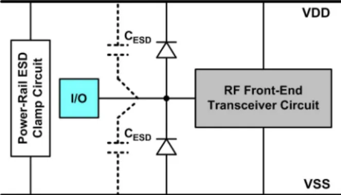
Fig. 1. Typical ESD protection scheme with double diodes for RF front-end or high-speed I/O applications.
(CESD) of the ESD protection devices must be minimized,
but the ESD robustness is still kept at the reasonable level [8]. ESD protection designs for RF front-end and high-speed I/O interface circuits must be optimized with consideration of parasitic capacitance and ESD protection capability.
A typical on-chip ESD protection scheme for RF front-end or high-speed I/O applications is shown in Fig. 1, where two ESD diodes at I/O pad are cooperated with the turn-on efficient power-rail ESD clamp circuit to discharge ESD current in the forward-biased condition. Through the turn-on efficient power-rail ESD clamp circuit, the device dimensions of these two diodes can be significantly shrunk to meet the circuit performance and ESD requirement simultaneously. In order to minimize the parasitic capacitance caused by the ESD protection diodes and to achieve satisfactory ESD robustness, the high frequency characteristics and the ESD levels of the ESD protection diodes in a 90-nm CMOS process were evaluated in this work to obtain the dependence of device size on ESD robustness and parasitic capacitance. Furthermore, the layout style of ESD protection diode will also directly affect its ESD robustness and parasitic capacitance. In previous studies [9]–[12], the ESD protection diodes realized in the waffle layout style have been verified to achieve better figure-of-merit (FOM) than that of stripe diodes under careful size optimization, which is suitable to RF front-end and high-speed I/O applications [9], [10].
Generally, the most important FOM used to evaluate the per-formance of the ESD protection diode isICP/CESD, whereICP
is the current level at which the measuredI–V curve deviates from its linearly extrapolated value by 20% [9]. Consequently, it is desired to implement the ESD protection diode with a 1530-4388/$26.00 © 2010 IEEE
YEH et al.: OPTIMIZATION ON LAYOUT STYLE OF ESD PROTECTION DIODE FOR CIRCUITS 239
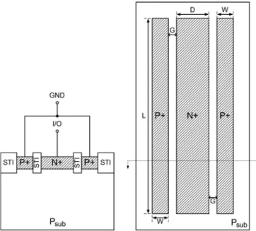
Fig. 2. Device cross-sectional view and layout top view of the ESD protection diode with typical stripe layout style.
large ratio of ICP/CESD. It is better for the ESD protection diode to achieve higher ICP and lower CESD at the specific layout style and device size. In order to further improve the
ICP/CESD, the area of active junction region in ESD protection
diode must be minimized to attain low parasitic capacitance, but its junction perimeter must be maximized to enhance the ESD robustness. In this work, the ESD protection diodes realized in stripe, waffle, octagon, waffle-hollow, and octagon-hollow layout styles are fabricated in a 90-nm CMOS process and com-pared with each other. According to the measured results, the ESD protection diodes with octagon and hollow layout styles can successfully boost theICP/CESDto make the diodes more profitable to RF front-end and high-speed I/O applications.
II. ESD PROTECTIONDIODES
For theN+/Psubdiode, the GND and I/O nodes are electri-cally connected toP+ diffusion and N+ diffusion, respectively. Under normal circuit operation, the diode is kept off due to the reverse-biased condition between the Psub andN+ diffusion regions. Although the diode is turned off, there is still an intrinsic junction capacitance of the diode seen by the signals at the I/O pad. On the other hand, the diode should be turned on to conduct ESD current at forward-biased condition under ESD stresses. Therefore, the junction capacitance of diode at reverse-biased condition and the ESD protection capability of diode at forward-biased condition are the important parameters to be investigated in the following.
A. Diode With Stripe Layout Style
The device cross-sectional view and layout top view of the ESD protection diodes with stripe layout style are shown in Fig. 2, which is the typical layout style to be often imple-mented in IC products. This typical stripe diode is realized with P+ stripe on both sides of the N+ stripe to give it with twice the conducting perimeter. Moreover, the width ofN+ stripe is
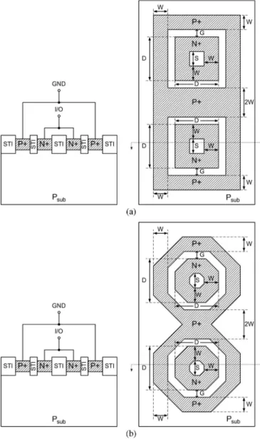
Fig. 3. Device cross-sectional view and layout top view of the ESD protection diodes with (a) waffle and (b) octagon layout styles.
twice as large as that of each P+ stripe because the width of N+ stripe is kept equal to the sum of each P+ stripe, in order to avoid the current crowding at theN+ stripe region. Based on the typical stripe diode, the diodes with the new proposed layout style will be discussed in the following sections to improve the characteristics of diodes for ESD protection and circuit performance.
B. Diodes With Waffle and Octagon Layout Styles
The device cross-sectional view and layout top view of the ESD protection diodes with waffle and octagon layout styles are shown in Fig. 3(a) and (b), respectively. The octagon layout style is formed from waffle layout style but the four corners are cut off. When the junction area of waffle and octagon diodes is reduced, they can achieve lower parasitic capacitance. Com-pared to the waffle diode, the junction perimeter and junction area of the octagon diode are simultaneously smaller than those of the waffle diode by 17%. It means that all FOMs based on physical characteristics of the waffle and octagon diodes would
240 IEEE TRANSACTIONS ON DEVICE AND MATERIALS RELIABILITY, VOL. 10, NO. 2, JUNE 2010
Fig. 4. Device cross-sectional view and layout top view of the ESD protection diodes with (a) waffle- and (b) octagon-hollow layout styles. The center region is drawn with the STI region to effectively reduce the parasitic capacitance. be totally the same. Fortunately, the risk of damages located at the corner can be reduced by forming octagon layout style because the corner angle of octagon diode is larger than that of waffle diode. Therefore, the octagon diode can be supposed to have better ESD level than waffle diode.
C. Diodes With Waffle- and Octagon-Hollow Layout Styles
The two new proposed diodes investigated in this study are illustrated in Fig. 4(a) and (b), which are called as the waffle-and octagon-hollow layout styles, respectively. Generally, the parasitic capacitance of the diode is proportional to the active junction area, and the ESD robustness is related to the active junction perimeter. For RF front-end and high-speed I/O appli-cations, the parasitic capacitance of the ESD protection diode is the key factor to directly affect the performance of RF front-end and high-speed I/O circuits. Therefore, it is desirable to implement the ESD protection diode with high ESD robustness but low parasitic capacitance.
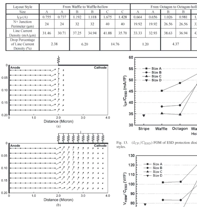
Fig. 5. Device cross-sectional view to explain ESD current flows in the diodes with (a) waffle and (b) waffle-hollow layout styles.
The purpose of forming the hollow layout is to reduce the active junction area and to keep the active junction perimeter at the same time by removing theN+ central diffusion region off. For instance, the cross-sectional views to explain ESD current flows in the diodes with waffle and waffle-hollow layout styles are shown in Fig. 5(a) and (b), respectively. According to the device cross-sectional view in Fig. 5(a), the ESD current could not uniformly flow through whole N+ active junction region in the waffle diode because the current always tends to flow through the shortest path between two nodes. Therefore, there is only a small part of total ESD current discharging through the N+ central diffusion region, where still contributes parasitic capacitance to RF front-end and high-speed I/O circuits at normal circuit operation. By removing theN+ central diffusion region to form the hollow layout style, the ESD current can be effectively concentrated in restricted region of the diode, as shown in Fig. 5(b). Consequently, the diodes with hollow layout style can be expected to attain a great reduction of parasitic capacitance without degrading ESD robustness severely at the same time. Similarly, all FOMs based on physical characteris-tics of the waffle-hollow are also the same as those of octagon-hollow diodes.
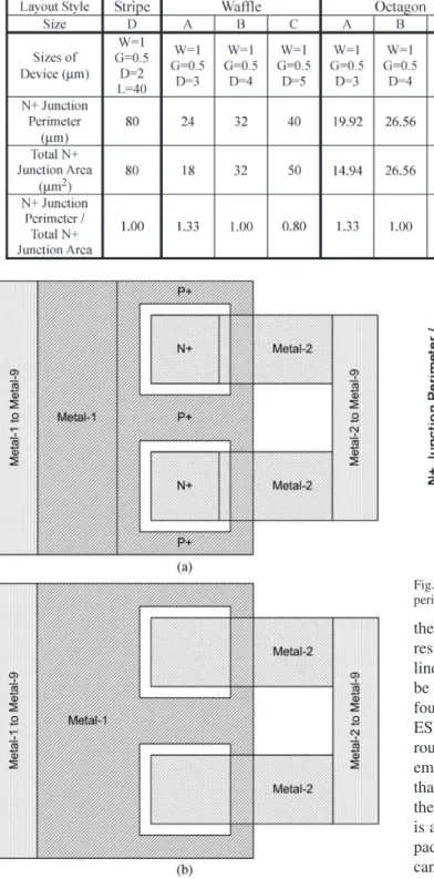
Based on the waffle layout style studied in previous works [9], [10], the octagon, waffle-hollow, and octagon-hollow lay-out styles are proposed and fabricated in a 90-nm CMOS process to investigate the dependence between ESD robustness and parasitic capacitance on diode layout styles. The important layout parameters of those investigated diodes are listed in Table I, where the different spacings are also marked in Figs. 2–4, respectively. It has to be noticed that the dimensions of the stripe diode in this work are not optimum.
YEH et al.: OPTIMIZATION ON LAYOUT STYLE OF ESD PROTECTION DIODE FOR CIRCUITS 241
TABLE I
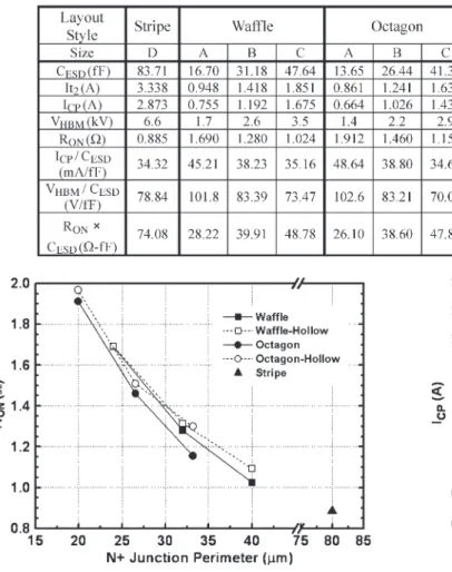
MEASUREDDEVICECHARACTERISTICS ANDPREVIOUSEVALUATIONVALUE OFDIODEUNDERDIFFERENTLAYOUTSTYLES
Fig. 6. Metal layout arrangement for the (a) interconnect routing of diodes and the (b) open pad structure.
D. Interconnect Routing of the Diodes
To effectively reduce the impact from the parasitic resistance and capacitance of the interconnect routing in the layout of ESD diodes, the arrangement of metal lines to connect the ESD diodes should be considered with the de-embedding operation. The layout scheme of interconnect routing of ESD diodes is shown in Fig. 6(a). The width of metal line from the diode to
Fig. 7. Performance evaluations with the factors of (N + junction perimeter)/(total N + junction area) under different diode layout styles. the pad is drawn as large as possible to reduce the parasitic resistance of interconnect routing. With the large width of metal line, the parasitic resistance of interconnect routing (that can be estimated manually with the sheet resistance provided by foundry) can be quite smaller than the turn-on resistance of the ESD diodes. About the parasitic capacitance of interconnect routing, the layout scheme of the open pad structure for de-embedding calculation is shown in Fig. 6(b). The metal-1 layer that was originally connected to P+ region is remained, and the metal-2 layer that was originally connected toN+ region is also remained. With the measuredS-parameters of the open pad structure, the parasitic capacitance of interconnect routing can be de-embedded to obtain the pure junction capacitance of the ESD diodes.
E. Performance Evaluations
Before implementing the diodes, there is a useful evaluation to imply the goodness of the diodes. This evaluation, discussed in the following paragraphs, is based on the physical dimen-sions of diodes listed in Table I.
This important evaluation is the factor of (N + junction perimeter)/(total N + junction area). This is the most com-monly used evaluation to estimate the diodes, as that illus-trated in Fig. 7. TheN+ junction perimeter is related to ESD
242 IEEE TRANSACTIONS ON DEVICE AND MATERIALS RELIABILITY, VOL. 10, NO. 2, JUNE 2010
Fig. 8. Layout top views for de-embedded calculation to extract the parasitic capacitance of the fabricated ESD diodes with (a) including- and (b) excluding-DUT patterns.
robustness, and the totalN+ junction area is corresponded to parasitic capacitance at normal circuit operation. Undoubtedly, this evaluation is expected to be large to sustain high enough ESD robustness and minimize the degradation of circuit per-formance for RF front-end and high-speed I/O applications. In Fig. 7, the diodes with hollow layout styles obviously have the highest values at the specified diode size. Moreover, the large-size diodes with hollow layout styles can achieve comparable level to that of small-size diodes with non-hollow layout style. This result inspires us to consider a way not to continuously shrink the diode size to avoid any capacitance penalty from the junction perimeter [8]–[10]. Although the diode with stripe layout style has the smallest width, its evaluation is not the highest because the diode with stripe layout style cannot give theN+ junction perimeter as much as those of the diodes with other layout styles. The performance evaluation is also listed in Table I.
III. EXPERIMENTALRESULTS
The test chips of diodes with the stripe, waffle, and new proposed layout styles have been fabricated in a 90-nm CMOS process. These diodes are prepared with the consideration of two-portS-parameter measurement, transmission line pulsing (TLP) measurement, and HBM ESD robustness measurement. In this work, each diode structure was tested four times from four separated dice.
A. Parasitic Capacitance
The diode devices are arranged with ground–signal–ground (G–S–G) pads to facilitate on-wafer two-portS-parameter mea-surement. During theS-parameter measurement, the P+ and N+ diffusion regions of the diode devices are connected to ports 1 and 2, respectively, and they are both biased at 0 V.
In order to extract the characteristics of the intrinsic device at high frequency, the parasitic effects of the pad and the interconnect routing must be de-embedded [13]–[15]. The test structures, one including the DUT and the other excluding
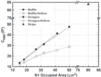
Fig. 9. Dependence ofCESDextracted fromS-parameter at 2.5 GHz under zero DC bias on theN+ occupied area of diode devices with different layout styles.
the DUT (open pad structure), as shown in Fig. 8(a) and (b), were implemented in the same test chip [13], [14]. The
Y22-parameter can be obtained from the measured two-port S-parameters by
Y22=Z (1 + S11)(1 − S22) + S12S21
0((1 + S11)(1 + S22) − S12S21) (1)
whereZ0is the termination resistance of 50Ω [15]. The mea-suredY -parameter of the including-DUT pattern is labeled as
Y22−meas, and the measured Y -parameter of the excluding-DUT pattern (open pad structure) is labeled as Y22−open. The intrinsic device characteristics, Y22−DUT, can be obtained by subtractingY22−openfromY22−meas. The parasitic capacitance (CESD) of each diode can be extracted from the Y -parameter
of the intrinsic device by
CESD=Im(Y222−DUTπf ) (2)
where f is the operating frequency. The extracted parasitic capacitances of the fabricated diode devices at 2.5 GHz under zero DC bias are listed in Table II and shown in Fig. 9.
From the measured results of the diode devices with stripe, waffle, and octagon layout styles, the extracted parasitic capac-itances are obviously proportional to the N+ occupied area. Meanwhile, the reductions of parasitic capacitances can achieve 16%, 26%, and 39% by modifying the diodes in sizes A, B, and C from waffle to waffle-hollow layout styles, respectively. Sim-ilarly, it can achieve the reductions of parasitic capacitance of 13%, 25%, and 38% by modifying the diodes from octagon to octagon-hollow layout styles. The reduction of parasitic capac-itance is exactly meeting the theoretical calculations. This great reduction of parasitic capacitance is the key factor to signifi-cantly improve the FOM of the diodes with hollow layout style.
B. Transmission Line Pulsing (TLP) Measurement
In order to investigate the device behavior during high ESD current stress, a transmission line pulsing (TLP) generator with a pulse width of 100 ns and a rise time of ∼2 ns is used
YEH et al.: OPTIMIZATION ON LAYOUT STYLE OF ESD PROTECTION DIODE FOR CIRCUITS 243
TABLE II
MEASUREDRESULTSAVERAGEDFROMFOURSEPARATEDDICE ANDFOMOFDIODEDEVICESWITHDIFFERENTLAYOUTSTYLES
Fig. 10. Dependence of TLP-measuredRONon theN+ junction perimeter of diode devices with different layout styles.
to measure the second breakdown current (It2) of the device [16]. For the ESD protection diode, it is suggested that an appropriate upper-bound current level,ICP, is utilized because the ESD protection diode should never be designed to discharge ESD current near its failure level [9], [10]. By using TLP, the on-resistance (RON), It2, and ICP derived from It2 of the diode devices under positive stresses at theP+ diffusion region with groundedN+ diffusion region are measured and listed in Table II. TheRONandICPversus theN+ junction perimeter of the diodes are illustrated in Figs. 10 and 11, respectively. Apparently, theRONis decreased and theICPis increased with the increasedN+ junction perimeter.
When the diode is modified from non-hollow to hollow layout style, the drop on ICP of the diode with large device size is greater than that of the diode with small device size. The line current densities, which are the ratio ofICP toN+ junc-tion perimeter, of waffle and octagon diodes are calculated in Table III. The drop percentages of line current density from waffle to waffle-hollow (from octagon to octagon-hollow) are also calculated in Table III. From the measured results and calculations, the waffle (or octagon) diode with large device size has larger line current density and larger drop percentage of line current density while modified to waffle-hollow (or octagon-hollow) diode. This implies that the ESD discharging
Fig. 11. Dependence of TLP-measuredICPon theN+ junction perimeter of diode devices with different layout styles.
current of waffle (or octagon) diode with large device size would flow more deeply through the N+ central diffusion region because waffle (or octagon) diode with large device size has more contacts at N+ diffusion region to cause a small equivalent resistance at the cathode. With more detailed explanation and illustration, the simulations can give a clear perspective. Fig. 12(a) and (b) are the current vector plots of the diode in small and large sizes, respectively. For convenience, the anode is set along the entire edge of the diode, and the cathode is set along the right half of the top surface of the diode. When the diode is drawn in small size, the fewer contacts at junction area make the current crowded into the nearest corner of the electrode. On the contrary, there are more contacts at the junction area for the diode drawn in large size, as shown in Fig. 12(b). The current crowding behavior experienced in Fig. 12(a) has diminished, and the current can be distributed through the entire electrode more widely. Based on the simu-lation results and the measured results of line current density in Table III, the ESD discharging current through the diode in large size is expected to flow more deeply through theN+ central diffusion region. Therefore, the diode in large device size has larger reduction of ICP when the diode with non-hollow layout style is modified to non-hollow layout style.
According to the measured results, the reductions ofICPare 2.4%, 6.2%, and 8.8% for the waffle diodes in sizes A, B, and
244 IEEE TRANSACTIONS ON DEVICE AND MATERIALS RELIABILITY, VOL. 10, NO. 2, JUNE 2010
TABLE III
LINECURRENTDENSITY OFDIODEDEVICES
Fig. 12. Simulated vectors of ESD discharging current along the cross section of waffle diode with (a) small and (b) large device sizes.
C, respectively. Also, they are 1.2%, 4.4%, and 10.6% for the octagon diodes in sizes A, B, and C, respectively. Compared with the reductions of parasitic capacitance, the removedN+ central diffusion region is originally flowed by a small part of total ESD discharging current. Consequently, removing the N+ central diffusion region of the diodes can greatly reduce the parasitic capacitance without degrading the ESD protection capability.
C. ESD Robustness
The human-body-model (HBM) ESD robustness of the fabri-cated diodes is also listed in Table II. The relationship between the HBM ESD level (VHBM) and theIt2based on the measured results in this work is about
VHBM≈ (1800 + RON) × It2 (3)
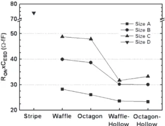
Fig. 13. (ICP/CESD) FOM of ESD protection diodes with different layout styles.
Fig. 14. (VHBM/CESD) FOM of ESD protection diodes with different layout styles.
where RON is the turn-on resistance of the diode. The HBM ESD levels of all ESD protection diodes are within the range of 1.4–3.5 kV, except the stripe diode.
D. FOM Comparison and Discussion
The FOMs (ICP/CESD, VHBM/CESD, andRON× CESD) of the diode devices are listed in Table II and shown in Figs. 13–15. The most important FOM,ICP/CESD, among the diodes is illustrated in Fig. 13. The trend ofICP/CESDis ap-parently increasing from non-hollow to hollow layout style due
YEH et al.: OPTIMIZATION ON LAYOUT STYLE OF ESD PROTECTION DIODE FOR CIRCUITS 245
Fig. 15. (RON× CESD) FOM of ESD protection diodes with different layout styles.
to the reduction of parasitic capacitance, and the results exactly meet the expectation of layout design. Because the HBM ESD level is directly proportional toIt2, the trend ofVHBM/CESD illustrated in Fig. 14 is quite similar to that in Fig. 13. According to the experimental results of diodes with different layout styles, the diodes with hollow layout styles can apparently achieve higher ESD robustness under the same parasitic capacitance. For instance, the measured results clearly demonstrate that the
ICP/CESDof waffle-hollow (or octagon-hollow) diode in size
C is better than that of waffle (or octagon) diode in size B. These two diodes actually have the same totalN+ junction area, but theN+ junction perimeter of waffle-hollow (or octagon-hollow) diode in size C is obviously larger. This feature reveals that the diodes with waffle-hollow (or octagon-hollow) layout styles can attain higher ICP than those with waffle (octagon) layout styles under the same totalN+ junction area to achieve betterICP/CESD. Besides, theICP/CESDcan also be slightly improved from waffle (or waffle-hollow) diode to octagon (or octagon-hollow) diode due to the relaxation of current distribu-tion located at the smoother corners.
TheICP/CESDvalues of waffle- and octagon-hollow diodes in sizes B and C can achieve almost the same level as that of waffle diode in size A. It represents that the diode with hollow layout style in large size still can sustainICP as high as that of the diode with waffle layout style in small size under the same parasitic capacitance. As a result, the waffle- and octagon-hollow diodes in large size can perform as well as the waffle diode in small size under careful layout optimization.
From TLP I–V measurement and the results in Fig. 11,
RONcan be reduced by increasing theN+ junction perimeter
of the ESD diodes, but this action also increases the parasitic capacitance of the ESD diodes simultaneously due to the in-creased N+ junction area. For ESD protection purposes, the
RON of the ESD diode is expected to be as small as better
to effectively clamp the voltage. The CESD is also highly demanded to be as small as better to avoid the RF circuits’ performance degradation. Therefore, the RON× CESD is an-other useful justification to the diodes, as shown in Fig. 15. The
RON× CESD value of the stripe diode is too large, which is
hard to be implemented for performance RF and
high-speed I/O interface applications. For the diodes with hollow layout styles, such values can be reduced to the range from 23 to 34(Ω − fF), which is much smaller than that of the stripe diode. Moreover, the RON× CESD value of the waffle- and octagon-hollow diodes in large size can also be comparable to that of waffle and octagon diodes with small size.
Although the waffle diode in small size theoretically has larger ratio of N+ junction perimeter to N+ junction area, carefully optimizing the size of waffle diode is still required to avoid any capacitance penalty from the junction perimeter [9], [10]. Therefore, it is not necessary to simply shrink the device size of waffle diode to achieve a high value ofICP/CESDand a low value ofRON× CESD. In this work, it has been verified that there are two methods, forming octagon and hollow layout styles, to effectively improve theICP/CESDandRON× CESD of the diodes.
IV. CONCLUSION
New proposed diodes with octagon and hollow layout styles have been successfully verified in a 90-nm CMOS process. Layout optimization is the essential element to minimize the parasitic capacitance and to improve ESD robustness of the ESD protection diodes for RF front-end and high-speed I/O applications. As compared to the diodes with stripe and waffle layout styles, the new proposed diodes with hollow layout styles have been demonstrated to significantly improve ESD robustness under the same parasitic capacitance. Therefore, the proposed waffle- and octagon-hollow diodes are more suitable to be implemented to RF front-end and high-speed I/O circuits.
ACKNOWLEDGMENT
The authors would like to thank the Editor and her review-ers for their valuable suggestions to improve this work for publication.
REFERENCES
[1] M. Mergens, G. Wybo, B. V. Camp, B. Keppens, F. D. Ranter, K. Verhaege, P. Jozwiak, J. Armer, and C. Russ, “ESD protection cir-cuit design for ultra-sensitive IO applications in advanced sub-90 nm CMOS technologies,” in Proc. IEEE Int. Symp. Circuits Syst., 2005, pp. 1194–1197.
[2] J. Wu, P. Juliano, and E. Rosenbaum, “Breakdown and latent damage of ultra-thin gate oxides under ESD stress conditions,” in Proc. EOS/ESD
Symp., 2000, pp. 287–295.
[3] S. Voldman, ESD: RF Technology and Circuits. New York: Wiley, 2006. [4] ESD Test Standard, ESD Association ESD STM5.1, 1998.
[5] ESD Test Standard, ESD Association ESD STM5.2, 1999.
[6] M.-D. Ker, T.-Y. Chen, and C.-Y. Chang, “ESD protection design for CMOS RF integrated circuits,” in Proc. EOS/ESD Symp., 2001, pp. 346–354.
[7] M. Natarajan, D. Linten, S. Thijs, P. Jansen, D. Tremouilles, W. Jeamsaksiri, T. Nakaie, M. Sawada, T. Hasebe, S. Decoutere, and G. Groeseneken, “RFCMOS ESD protection and reliability,” in Proc.
IEEE Int. Symp. Phys. Failure Anal. Integr. Circuits, 2005, pp. 59–66.
[8] Y.-W. Hsiao and M.-D Ker, “Low-capacitance ESD protection design for high-speed I/O interfaces in a 130-nm CMOS process,” Microelectron.
Reliab., vol. 49, no. 6, pp. 650–659, Jun. 2009.
[9] K. Bhatia and E. Rosenbaum, “Layout guidelines for optimized ESD protection diodes,” in Proc. EOS/ESD Symp., 2007, pp. 19–27. [10] K. Bhatia, N. Jack, and E. Rosenbaum, “Layout optimization of ESD
protection diodes for high-frequency I/Os,” IEEE Trans. Device Mater.
246 IEEE TRANSACTIONS ON DEVICE AND MATERIALS RELIABILITY, VOL. 10, NO. 2, JUNE 2010
[11] R. M. D. A. Velghe, P. W. H. de Vreede, and P. H. Woerlee, “Diode network used as ESD protection in RF applications,” in Proc. EOS/ESD
Symp., 2001, pp. 337–345.
[12] S. Dabral and K. Seshan, “Diode and transistor design for high speed I/O,” U.S. Patent 7 012 304, Mar. 14, 2006.
[13] C.-Y. Lin, M.-D. Ker, and G.-X. Meng, “Low-capacitance and fast turn-on SCR for RF ESD protection,” IEICE Trans. Electron., vol. E91-C, no. 8, pp. 1321–1330, Aug. 2008.
[14] M.-D. Ker and C.-Y. Lin, “Low-capacitance SCR with waffle layout struc-ture for on-chip ESD protection in RF ICs,” IEEE Trans. Microw. Theory
Tech., vol. 56, no. 5, pp. 1286–1294, May 2008.
[15] D. M. Pozar, Microwave Engineering, 3rd ed. New York: Wiley, 2005. [16] T. J. Maloney and N. Khurana, “Transmission line pulsing techniques for
circuit modeling of ESD phenomena,” in Proc. EOS/ESD Symp., 1985, pp. 49–54.
Chih-Ting Yeh received the B.S. degree from the Department of Electrophysics, National Chiao Tung University, Hsinchu, Taiwan, in 2004 and the M.S. degree from the Institute of Electronics, National Chiao Tung University, in 2006, where he is cur-rently working toward the Ph.D. degree in electronics engineering.
Since 2007, he has been an ESD Protection sign Engineer with the Department of Circuit De-sign, Design Automation Technology Division, SoC Technology Center, Industrial Technology Research Institute, Hsinchu. His major research topic is the on-chip ESD protection design of CMOS integrated circuits.
Ming-Dou Ker (S’92–M’94–SM’97–F’08) received the Ph.D. degree from the Institute of Electronics, National Chiao Tung University, Hsinchu, Taiwan, in 1993.
He was the Department Manager with the Com-puter and Communication Research Laboratories, VLSI Design Division, Industrial Technology Re-search Institute (ITRI), Hsinchu. Since 2004, he has been a Full Professor with the Institute of Electronics, National Chiao Tung University. From 2006 to 2008, he served as the Director of Master Degree Program with the College of Electrical Engineering and Computer Science, National Chiao Tung University, as well as the Associate Exec-utive Director of National Science and Technology Program on System-on-Chip (NSoC) in Taiwan. Since 2008, he was rotated to serve as the Chair Professor and the Vice President with I-Shou University, Kaohsiung, Taiwan. He had been invited to teach and/or consulted on the reliability and quality design for integrated circuits by hundreds of design houses and semiconductor companies in the worldwide IC industry. In the field of re-liability and quality design for circuits and systems in CMOS technology, he has published over 380 technical papers in international journals and conferences. He has proposed many solutions to improve the reliability and quality of integrated circuits, which have been granted with 158 U.S. patents and 146 Taiwan patents. His current research interests include reliability and quality design for nanoelectronics and gigascale systems, high-speed and mixed-voltage I/O interface circuits, on-glass circuits for system-on-panel applications, and biomimetic circuits and systems for intelligent prosthesis.
Prof. Ker has served as a member of the Technical Program Committee and the Session Chair of numerous international conferences. He ever served as an Associate Editor for the IEEE TRANSACTIONS ONVLSI SYSTEMS. He was selected as the Distinguished Lecturer in the IEEE Circuits and Systems Society (in 2006–2007) and in the IEEE Electron Devices Society (in 2008–2010). He was the President of Foundation in the Taiwan ESD Association. In 2008, he has been elevated as an IEEE Fellow “for his contributions to the electrostatic protection in integrated circuits and the performance optimization of VLSI microsystems.” In 2009, he was awarded as one of the top ten Distinguished Inventors in Taiwan and one of the top hundred Distinguished Inventors in China.
Yung-Chih Liang received the B.S. and M.S. de-grees in electrical engineering from the National Chi Nan University, Nantou, Taiwan, in 2002 and 2004, respectively.
Since 2005, he has been a Circuit Design Engi-neer with the Circuit Design Department, Design Automation Technology Division, SoC Technology Center, Industrial Technology Research Institute, Hsinchu, Taiwan. His current research interests in-clude on-chip ESD protection circuit design and analog/digital circuits.