半導體中場操控之自旋流與自旋堆積
176
0
0
全文
(2) Field manipulations of spin flow and spin accumulation in semiconductors Lu Yao Wang January 26, 2008.
(3) 半導體中場操控之自旋流與自旋堆積 研究生:王律堯. 指導教授:朱仲夏. 國立交通大學電子物理研究所. 摘要 本論文旨在探討與了解在半導體中運用數種純電性方式來產生和操控自旋流與 自旋堆積之現象。我們研究了在彈道傳輸與擴散範疇中,Rashba 和 Dresselhaus 本質自旋軌道交互作用對電子自旋的影響。在彈道傳輸的 Rashba 量子窄通道 中,我們論證了自旋流可以藉由時變指狀閘極所產生之時變調制的 Rashba 自旋 係數來產生。我們也建構了反彈散射效應對此自旋流堅實性質的影響。在擴散半 導體的條狀系統中,我們論證了在自旋霍爾電場中,Dresselhaus 自旋軌道交互 作用的確會引起條狀系統橫向邊緣的自旋堆積。更進一步,我們探討在外加一個 平面弱磁場下,由 Dresselhaus 自旋軌道交互作用產生之自旋特性。當外加磁場 沿著電場方向時,自旋堆積 Sz 是此磁場的偶函數﹔當外加磁場沿著條狀系統的 橫方向時,自旋堆積 Sz 對磁場的關係變成不對稱。我們發現此一自旋軌道的磁 效應可以當作鑑別不同自旋軌道機制的一個工具。類似在一個侷域的散射子附近 所形成的 Landauer 電偶極矩,我們也發現在沒有塊材自旋流存在的 Rashba 自旋 軌道交互作用的系統中,一個正常的散射子附近仍會有自旋偶極的存在,這個結 果吻合一般理論結果﹕在擴散範疇中 Rashba 自旋軌道交互作用的系統中沒有自 旋堆積 Sz 在樣品橫向邊緣。. i.
(4) FIELD MANIPULATIONS OF SPIN FLOW AND SPIN ACCUMULATION IN SEMICONDUCTORS Student: Lu Yao Wang. Advisor: Chon-Saar Chu Department of Electrophysics National Chiao-Tung University. Abstract The thesis of this work is to explore and to understand various ways of generating and manipulating spin flow and spin accumulation in a semiconductor by pure electrical means. Taking the intrinsic spin-orbit interaction (SOI) such as the Dresselhaus SOI and the Rashba SOI as our major wrenches on the electron spin, we focus upon two different regimes: the ballistic and the diffusive regimes. In a ballistic Rashba-type quantum channel, we demonstrate that time-modulation of the Rashba SOI coupling parameter, via an ac-biased finger gate, leads to a dc spin current. That this dc spin current is robust against elastic backscattering is also established. In a diffusive semiconductor stripe, we show that the Dresselhaus SOI does lead to spin accumulation at the lateral edges in a spin-Hall electric field. Further signature of the Dresselhaus SOI is explored by introducing a weak in-plane magnetic field. The spin accumulation Sz is an even function of magnetic field when it is longitudinal, pointing along the driving electric field direction. For a transverse magnetic field, when it is pointing parallel to the width of the stripe, the spin accumulation becomes asymmetric. Our finding thus provide a basis for the establishment of a SOI mechanism diagnostic tool out of the magnetic field effect on the spin accumulation. Furthermore, we find that, in analogy with the Landauer charge dipole around a local scatterer, a spin dipole can exist around a normal scatterer in a Rashbatype 2DEG host where the bulk spin-Hall current is known to be zero. The prediction of these spin dipoles is consistent with another known fact: that no macroscopic spin accumulation occurs at the lateral sample edges in the case of Rashba SOI. ii.
(5) 致謝 首先我必須感謝父母多年來的鼓勵與栽培讓我得以完成博士學位,誠摯的感謝我 的指導教授朱仲夏老師多年的指導與教誨,也同時感謝唐志雄教授以及 A.G. Mal’shukov 教授的指導與幫助,讓我得以完成此博士論文﹔感謝許多家裡的親戚 支持我讀博士班。 感謝林高進、邱裕煌和鄔其君學長和實驗室的同學榮興、淑維、吉偉,學弟妹: 淑娟、宇廷、昱佑、哲民、靖航、冠伊、志宣、昆宜、冠誼、智偉在日常生活的 激勵與幫助。 感謝一群好友:俊成、曉菁夫婦,銘哲、淑媚夫婦, 秉忠、文泰、高毅、添全、國 勝、榮民、佩宜、瓊姿、琪郎、姜勇、建霆、政煌…等人的相挺﹔還有很多朋友 列不完衷心的感謝他(她)們。. iii.
(6) Contents 1 Introduction. 1. 1.1. Introduction to background . . . . . . . . . . . . . . . . . . . . . . . . . .. 1. 1.2. Spin-orbit coupling in the semiconductor system . . . . . . . . . . . . . . .. 3. 1.3. Electrical means of spin manipulations through SOI in ballistic and diffusive systems . . . . . . . . . . . . . . . . . . . . . . . . . . . . . . . . . . .. 7. 1.4. Historical introduction to spin-Hall effect . . . . . . . . . . . . . . . . . . .. 8. 1.5. Motivations . . . . . . . . . . . . . . . . . . . . . . . . . . . . . . . . . . . 10. 1.6. A guiding tour to this thesis . . . . . . . . . . . . . . . . . . . . . . . . . . 14. 2 Dc spin current generation in a Rashba-type ballistic quantum channel 17 2.1. Introduction . . . . . . . . . . . . . . . . . . . . . . . . . . . . . . . . . . . 18. 2.2. The generation of a spin current via ac-biased FG in the RQC . . . . . . . 22. 2.3. One-sideband approximation of the single ac-biased FG in the weak pumping regime . . . . . . . . . . . . . . . . . . . . . . . . . . . . . . . . . . . . 27. 2.4. Numerical results for the ac-biased FG in a RQC . . . . . . . . . . . . . . 29. 2.5. The backscattering effect of dc SC generation in a RQC . . . . . . . . . . . 33. 2.6. Numerical results for the backscattering effect of a SC generation . . . . . 36. 2.7. Summary . . . . . . . . . . . . . . . . . . . . . . . . . . . . . . . . . . . . 38. 3 Derivation of the spin diffusion equation: a nonequilibrium Green’s function approach 3.1. 42. Introduction . . . . . . . . . . . . . . . . . . . . . . . . . . . . . . . . . . . 42 iv.
(7) CONTENTS 3.2 Theory of the spin density in the diffusion regime . . . . . . . . . . . . . . 44 3.2.1. Green’s function in the presence of the SOI . . . . . . . . . . . . . . 44. 3.2.2. Green’s function in the presence of disorder with the SOI . . . . . . 46. 3.3. Diffusion equation for spin densities with an in-plane magnetic field . . . . 48. 3.4. Theory of the spin current in the diffusion regime . . . . . . . . . . . . . . 61. 3.5. Summary . . . . . . . . . . . . . . . . . . . . . . . . . . . . . . . . . . . . 65. 4 The intrinsic spin-Hall effect without the magnetic field on a two-dimensional strip. 66. 4.1. Introduction . . . . . . . . . . . . . . . . . . . . . . . . . . . . . . . . . . . 67. 4.2. The diffusion equations of the spin densities for intrinsic SHE . . . . . . . 69. 4.3. The spin currents for the intrinsic SHE . . . . . . . . . . . . . . . . . . . . 71. 4.4. The solutions of spin densities in the case of Dresselhaus SOI . . . . . . . . 72. 4.5. Numerical results and discussions . . . . . . . . . . . . . . . . . . . . . . . 73. 4.6. Summary . . . . . . . . . . . . . . . . . . . . . . . . . . . . . . . . . . . . 79. 5 The intrinsic spin-Hall effect with an in-plane magnetic field on a twodimensional strip. 82. 5.1. Introduction . . . . . . . . . . . . . . . . . . . . . . . . . . . . . . . . . . . 83. 5.2. The diffusion equations for the intrinsic SHE with an in-plane magnetic field 85. 5.3. Theory of the spin current in the diffusion regime . . . . . . . . . . . . . . 88. 5.4. The solutions of spin densities with the in-plane magnetic field for the case of Dresselhaus SOI . . . . . . . . . . . . . . . . . . . . . . . . . . . . . . . 90. 5.5. Numerical results and discussions . . . . . . . . . . . . . . . . . . . . . . . 91. 5.6. Summary . . . . . . . . . . . . . . . . . . . . . . . . . . . . . . . . . . . . 96. 6 Spin-Hall interface resistance in terms of Landauer-type spin dipoles. 99. 6.1. Introduction . . . . . . . . . . . . . . . . . . . . . . . . . . . . . . . . . . . 99. 6.2. Spin cloud induced by a single impurity . . . . . . . . . . . . . . . . . . . . 101. v.
(8) CONTENTS 6.3 Spin accumulation in the semi-infinite system with a boundary at y=0 . . 112 6.4. Spin-Hall resistance and energy dissipation . . . . . . . . . . . . . . . . . . 116. 6.5. Summary . . . . . . . . . . . . . . . . . . . . . . . . . . . . . . . . . . . . 117. 7 Conclusion and future work. 118. 7.1. Conclusion . . . . . . . . . . . . . . . . . . . . . . . . . . . . . . . . . . . . 118. 7.2. Future works . . . . . . . . . . . . . . . . . . . . . . . . . . . . . . . . . . 120. A Transformation of the wave function in region (II). 122. B Numerical method to solve the transmission and reflection amplitudes 124 C One-side band approximation in the weak pumping regime. 128. D Fourier transformation of the four density. 131. E Detailed calculation for the spin-Hall current and the charge current 135 E.1 Spin-Hall current . . . . . . . . . . . . . . . . . . . . . . . . . . . . . . . . 135 E.2 Charge current along the x axis . . . . . . . . . . . . . . . . . . . . . . . . 142 F Derivation of the vertex T(p). 145. G Detailed calculation for source terms I n (q). 148. vi.
(9) List of Figures 1.1 Magnetoresistance of three Fe/Cr superlattices at 4.2 K. The current and applied field are along the same [110] axis in the plane of the layers. (PRL, 61, 2427 (1988)) 1.2. . . . . . . . . . . . . . . . . . . . . . . . . . . . . . . . .. 2. (a)With the gate voltage off, the aligned spins pass through the channel and are collected in the other side. (b)With the gate voltage on: if spins are not aligned with the direction of magnetization of the collector, no current can pass. In this way, the emitter-collector current is modulated by gate electrode. . . . . . . . . . . . . . . . . . . . . . . . . . . . . . . . . . . . .. 1.3. 4. The red and green arrows denote the electron spin and momentum, respectively. In the presence of an electric field the Fermi surface (circle) is displaced an amount |eEx t0 /~|at time t0 (shorter than typical scattering times). While moving in momentum space, electrons experience an effective torque which tilts the spin up for py > 0 and down for py < 0, creating a spin current in the y direction.(Phys. Rev. Lett. 92, 126603 (2004)). . . 10. 1.4. (A and B) Two-dimensional images of spin density ns and reflectivity R, respectively, for unstrained GaAs sample measured at T=30 K and E=10 mV/µm (Science 306, 1910 (2004)). . . . . . . . . . . . . . . . . . . . . . . 11. 2.1. (a) Top-view schematic illustration of the RQC. The ac-biased FG, of width l , is indicated by the gray area; (b) the electron dispersion relation of an unperturbed RQC. . . . . . . . . . . . . . . . . . . . . . . . . . . . . . . . 20. vii.
(10) LIST OF FIGURES 2.2 The wave functions can be separated by three different regions (I)(x < −l/2), (II) (−l/2 < x < l/2), and (III) (x > l/2). The region (II) includes the static and dynamic Rashba spin-orbit coupling constant. . . . . . . . . 25 2.3. ↑ ↓ Spin-resolved current transmissions TRL (red-solid) and TRL (blue-dashed). versus the incident energy µ/Ω. Parameters N =1, α0 =0.13, Ω=0.002, l=20, and α1 =(a) 0.03, (b) 0.04, and (c) 0.05. The corresponding dc SC is plotted in (d). . . . . . . . . . . . . . . . . . . . . . . . . . . . . . . . . . . 30 2.4. The configuration of two ac-biased FGs is illustrated with a tunable phase difference φ. . . . . . . . . . . . . . . . . . . . . . . . . . . . . . . . . . . . 31. 2.5. Current transmission versus µ/Ω for N =(a) 1, and (b) 2. Pumped spins per cycle are plotted in (c) for N =1 (thick curve) and N =2 (thin curve) with α1 =0.065, and driving frequency Ω=0.001. Other parameters are the same as in Fig. 2.3. . . . . . . . . . . . . . . . . . . . . . . . . . . . . . . . 32. 2.6. Pumped spin current and charge currents in unit of nA are plotted as a function of phase difference φ. Other parameters are α0 = 0.13, α1 = 0.065, and the oscillating frequency Ω = 0.002. The FG width is l =20 and the separation distance ∆l =20. The solid (blue) and dashed (red) curves denote the spin current and CC, respectively. . . . . . . . . . . . . . . . . . 34. 2.7. Top-view schematic illustration of the RQC with a static barrier. The acbiased FG, of width l, is indicated by the shaded area. The elastic scatterers are sketched by long-solid line of type A and short-solid line of type B. . . 35. 2.8. The SC and CC are plotted as a function of channel width d. The static full-barrier is located (a) inside and (b) outside the FG with various longitudinal positions. The empty-symbols and filled-symbols indicate the SC and the CC, respectively. The Fermi energy is fixed at E =0.0131 and other parameters are α0 = 0.13, α1 =0.03, l =20, Ω =0.002, and V0 =0.1. The center and the edges of the time-modulated regions are at x0 =0, ±10, respectively. . . . . . . . . . . . . . . . . . . . . . . . . . . . . . . . . . . . 39 viii.
(11) LIST OF FIGURES 2.9 The repulsive, (a)-(c) and attractive, (d)-(f), partial-barrier is located at the FG center but with various V0 . We choose V0 =0.1, 0.2, -0.1, -0.2, in (a), (b), (d), (e), respectively. The current transmission is plotted as incident energy in the unit of µ/Ω. Other parameters are α0 =0.13, α1 =0.03, Ω =0.002, l =20, and d = 40. . . . . . . . . . . . . . . . . . . . . . . . . . 40 3.1. Top-view schematic illustration of the 2D strip with a width d. The longitudinal driving electric field is applied in the x-axis. The tunable in-plane magnetic field Bk can be applied in this 2D strip. The angle θ is between the in-plane magnetic field and the electric field. . . . . . . . . . . . . . . . 43. 4.1. The 2D strip of the width d is applied a electric field along x axis. The transverse boundaries at y = ±d/2. . . . . . . . . . . . . . . . . . . . . . . 68. 4.2. Spin densities Sz± (1/µm2 ) and spin-Hall current ISH in unit of τ βkF2 N0 eED/(~lso ) are plotted as a function of X = nw2 for various quantum well thickness: (a) w = 2 × 10− 8m, (b) 2.5 × 10− 8m, and (c) 3 × 10− 8m. Sz± is the spin accumulations for y = d/2 and y = −d/2, respectively. These bold(red) arrows indicate the allowed ranges of parameter X: (a) 10.4 < X < 47.28, (b) 0 < X < 47.28, and (c) 0 < X < 47.28. The corresponding electron density is given by n = X/w2 . . . . . . . . . . . . . . . . . . . . . . . . . . 75. 4.3. Spin densities ∆Sx (y = d/2) are plotted as a function of the strip width d in unit of lSO for various values of X(κ/kF ) in a fixed w = 3w0 , where the unit of thickness denotes w0 = 1 × 10⁻⁸ m. The blue (solid), red (dashed), and green (dotted) curves are represented for X =22, 30, and 40, respectively. The spin densities ∆Sx (y = −d/2) have the same values with respect to ∆Sx (y = d/2) due to even parity property of ∆Sx (y). . . . . . . . . . . . . 77. ix.
(12) LIST OF FIGURES 4.4 Spin densities ∆Sz (y = d/2) are plotted as a function of the strip width d in unit of lSO for various values of X(κ/kF ) in a fixed w = 3w0 , where the unit of thickness denotes w0 = 1 × 10⁻⁸ m. The blue (solid), red (dashed), and green (dotted) curves are represented for X =22, 30, and 40, respectively. The spin densities ∆Sz (y = −d/2) have the same values but opposite sign with respect to ∆Sz (y = d/2) due to odd parity property of ∆Sz (y). . . . . 78 4.5. Total spin densities Sx (y) are plotted as a function of transverse coordinate y in unit of lso . The blue (solid), red (dashed), and green (dotted) curves are represented for X = 22, 30, and 40, respectively. The total spin densities b(0). Sx (y) exhibit the symmetric behavior. The bulk values of Sx. depend on. the values of X. . . . . . . . . . . . . . . . . . . . . . . . . . . . . . . . . . 80 4.6. Total spin densities Sz (y) are plotted as a function of transverse coordinate y in unit of lso . The blue (solid), red (dashed), and green (dotted) curves are represented for X = 22, 30, and 40, respectively. The total spin densities b(0). Sz (ξ) exhibit the anti-symmetric behavior. The bulk values of Sz the absence of an in-plane magnetic field. 5.1. = 0 in. . . . . . . . . . . . . . . . . . . 81. Top-view schematic illustration of the 2D strip with a width d. The longitudinal driving electric field is applied in the x-axis. The tunable in-plane magnetic field Bk can be applied in this 2D strip. The angle θ is between the in-plane magnetic field and the electric field. . . . . . . . . . . . . . . . 85. 5.2. Spin densities Si are plotted as a function of y in the unit of lso for a fixed w = 3 × 10⁻⁸ m in various Bx . Other parameters are X = 22 and the electron density n = 2.4 × 10¹⁵ (1/m2 ). Each panel shows the different curves with parameters Bx = −300mT (black-triangle), B = 0 (blue-solid) and Bx = 300mT (red-dashed). Spin densities Sx , Sy and Sz in the unit of 1/µm2 are shown in (a), (b) and (c), respectively. . . . . . . . . . . . . . . 93. x.
(13) LIST OF FIGURES 5.3 Spin densities Si are plotted as a function of y in the unit of lso for a fixed w = 3 × 10⁻⁸ m in various By . Other parameters are X = 22 and the electron density n = 2.4 × 10¹⁵ (1/m2 ). Each panel shows the different curves with parameters By = −300mT (black-triangle), B = 0 (blue-solid) and By = 300mT (red-dashed). Spin densities Sx and Sz in the unit of 1/µm2 are shown in (a) and (b), respectively. . . . . . . . . . . . . . . . . 94 5.4. The spin densities Si± is plotted as a function of the magnetic field Bx and By for i = x, y, and z. The quantum well thickness w = 3 × 10⁻⁸ m is fixed for X = 22. The notation Si± denotes the spin density Si at y = ±d/2. . . 97. 5.5. The contour feature of the spin density Sz is plotted as a function of y versus the (a) longitudinal magnetic field Bx and (b) transverse magnetic field By . The 2D strip edges are from y = −5 to y = 5. . . . . . . . . . . . 98. 6.1. Examples of diagrams for the spin density Sz . Scattering of electrons by the target impurity is shown in the solid circles. Dashed lines denote the ladder series of particles scattered by the background random impurities. p, k, and k0 represent the electron momenta. . . . . . . . . . . . . . . . . . 104. 6.2. The constructions of diagram (a) of Fig. 6.1 are decomposed into ladder series. . . . . . . . . . . . . . . . . . . . . . . . . . . . . . . . . . . . . . . 105. 6.3. Spatial distribution of Sz component of the spin density around a single scatterer. The unit of length is lso . . . . . . . . . . . . . . . . . . . . . . . 111. D.1 The time loop ordering is shown in this figure. The state evolves from −-branch to +-branch. . . . . . . . . . . . . . . . . . . . . . . . . . . . . . 133 (1)l. E.1 The diagram of Ii. shows that average retarded (advanced) Green’s func-. tion Gr (Ga ) can be expanded by summing over all unperturbed Green’s function G(0)r (G(0)a ) in ladder series. The dashed lines denote the interaction of impurities. . . . . . . . . . . . . . . . . . . . . . . . . . . . . . . . 137. xi.
(14) LIST OF FIGURES (2)l. E.2 The diagram of Ii. shows that average retarded (advanced) Green’s func-. tion Gr (Ga ) can be expanded by summing over all unperturbed Green’s function G(0)r (G(0)a ) in ladder series. The dashed lines denote the interaction of impurities. . . . . . . . . . . . . . . . . . . . . . . . . . . . . . . . 139 F.1 The diagram of T (p) can be decomposed into several diagrams connecting to ki /m∗ and N , where N ≡ ∂(h · σ)/∂k i . . . . . . . . . . . . . . . . . . . 147 G.1 The diagram of I1n is plotted in case of q = 0. . . . . . . . . . . . . . . . . 149 G.2 The diagram of I1n is plotted in case of small q. . . . . . . . . . . . . . . . 151 G.3 The diagram of I2n is plotted in case of q = 0. . . . . . . . . . . . . . . . . 153 G.4 The diagram of I2n is plotted in case of small q. . . . . . . . . . . . . . . . 155. xii.
(15) Chapter 1 Introduction 1.1. Introduction to background. Traditional electronic devices depend on the transport of charges in semiconductors. Most recently, scientists try to develop devices based on the electron ’spin’ rather than the electron charge. It becomes very remarkable to buildup a new generation of spin-based devices. Since the fabrication technology of the semiconductor become very ingenious and functional, more and more quantum devices can be achieved and a lot of hidden quantum phenomena are excavated. These electronic devices have been widely applied on industry and those devices are based on the macroscopic electron dynamics. It has been found another possible way in the use of the electron spin to construct the spin-based quantum devices and modulate the spin dynamics via the conventional electric means. Spin is the only internal degree of freedom of an electron and conventional semiconductor devices are based on the electron charge. One can merge spin and electron dynamics into spintronics in the semiconductor and provide electronics devices with new functionalities and achieving quantum computing via reliable spintronics based on the electron spin[1, 2]. Both theory and experiments succeed in impressive progress in the spintronics field in recent years. However, the high challenges and difficulties still exist and have to be solved by developing the theory and experimental techniques such as ”enhancement of the spin. 1.
(16) CHAPTER 1. INTRODUCTION. Figure 1.1: Magnetoresistance of three Fe/Cr superlattices at 4.2 K. The current and applied field are along the same [110] axis in the plane of the layers. (PRL, 61, 2427 (1988)) coherent length”, and ”suppression of the spin relaxation”. The first application of the spin-based device is fabricated by the magnetic materials and use the effect of giant magnetoresistance (GMR)[3, 4]. This effect was observed in the structures of ferromagnetic-nonmagnetic-ferromagnetic layers by Albert Fert and Peter Gunberg in 1988. The magnetoresistance of GMR materials can be largely decreased via a weak magnetic field (see Fig. 1.1). This technique has been realized for write-in and read-out data from the hard-disk. More recent research focus on the challenge of creating spintronics devices in semiconductor configurations without magnetic materials and applying magnetic fields. To control electron spins in electric means can be achieved by the spin-orbit interaction (SOI). Datta and Das proposed a simple model of spin-transistor in which the electron spin can transport and precess via SOI from a ferromagnetic source injecting into semiconductor to reaching a ferromagnetic drain [5]. In this spin-transistor, the polarization of the electron spin depends on the strength of spin-orbit interaction (SOI) which can be tuned by applying a gate voltage. Because the spin polarization parallel to the polarization of the. 2.
(17) CHAPTER 1. INTRODUCTION drain can pass through the channel, one can tune the voltage to modulate the current flow for ’on-’ or ’off-’state. However, the difficulty of Datta-Das transistor is the very low injection rate (∼ 1 percentage) for electron spins injecting from the magnetic metal into the semiconductor [6, 7]. This difficulty for spin injection from a magnetic metal into a semiconductor originates from the conductivity mismatch between these materials [8]. Because the spin injection coefficient γ is proportional to σN /σM leading to γ ¿ 1 in the diffusive regime, where σN and σM are conductivities of the normal (N) (semiconductor) and magnetic metallic (M) contacts, respectively. The low spin injection rate can be enhanced by inset a tunnel contact between a magnetic metal and a semiconductor [9]. However, combining with metallic, tunnel, and semiconductor contacts is inconvenient and complicated fabrications. Because the strength of SOI is much larger in semiconductors than in vacuum, building up the all-semiconductor devices provides a possible solution for conductivities mismatch between NM junction. In this way, the manipulation of electron spins through the SOI can be achieved in all electric means. Basically, the transport behavior of electron spins can be investigated in the ballistic regime and in the diffusive regime. The former concentrates on the interference between wave functions of spinors through an external field because the spin relaxation time is much larger than the scattering time. The latter one concentrates on the macroscopic coupling-behavior between electric current and spins through an external field because the spin relaxation time is much smaller than the scattering time. The enhancement of SOI would be discussed in semiconductors in next section.. 1.2. Spin-orbit coupling in the semiconductor system. We start from Dirac’s equation and extend it to semiconductors in order to understand the importance of SOI in the solid state community. Electron spin is the only internal degree of freedom of electrons following naturally from the Dirac equation when Dirac tried to put wave function in a covariant form, when space and time appear on equal footing. A. 3.
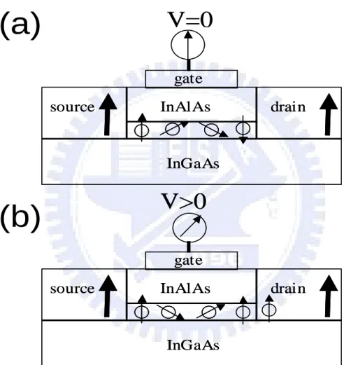
(18) CHAPTER 1. INTRODUCTION. V=0. (a). gate source. InAlAs. drain. InGaAs. V>0. (b). gate source. InAlAs. drain. InGaAs. Figure 1.2: (a)With the gate voltage off, the aligned spins pass through the channel and are collected in the other side. (b)With the gate voltage on: if spins are not aligned with the direction of magnetization of the collector, no current can pass. In this way, the emitter-collector current is modulated by gate electrode.. 4.
(19) CHAPTER 1. INTRODUCTION non-relativistic limit of the Dirac equation gives rise to the spin-orbit interaction term, a term that has found great success in atomic energy spectra. In vacuum, the form of this spin-orbit interaction can be expressed by [10]. HSO =. −e~ ~ σ · (E × p) = σ · (∇V × p) 2 2 4m0 c 4m20 c2. (1.1). where m0 is the free electron mass, ~ is the Plank’s constant and c is the light speed. This term HSO can be interpreted that an electron moving in an electric potential region sees, in its frame of reference, an effective magnetic field which couples with the electron spin through the magnetic moment of the electron spin. Through this effective magnetic field, which certainly depends on the orbital motion of the electron, the SOI is established. This physics holds in semiconductor too, when V(r) becomes the periodic potential of the host lattice and also the impurities. Electronic state calculation in semiconductor can be properly described by the k · p model, when we investigate physical effect in the vicinity of the band edges. Furthermore, within the envelope function approximation (EFA), the energy band can be characterized by effective masses. The model of EFA is valid to describe the electron states in the presence of electric and magnetic field that vary slowly on the length of lattice constant. While there is an build-in effective electric field in the material, the SOI naturally occurs in this semiconductor. Such effective electric field can be divided into the contribution from the build-in crystal field due to bulk inversion asymmetric (BIA) the so-called Dresselhaus SOI [11], or structural inversion asymmetry (SIA), the so-called Rashba SOI [12]. The BIA is found in zincblende structure and the SIA in asymmetric quantum wells (QWs) or heterostructures. In use of the effective mass approximation, all the fast-varying atomic potential has been included into the effective mass. Slower variation of V(r), its variation length scale much larger than the lattice spacing, is found to contribute to SOI with a much larger SO coupling constant λ. For a central potential V(r) depends on only r without angular. 5.
(20) CHAPTER 1. INTRODUCTION dependence in vacuum, the SO coupling can be recognized as L λvac 1 dV ~ ~ 1 dV ~ 1 dV σ·(∇V × p) = σ·(r × p) = σ· = − L·σ (1.2) 2 2 2 2 2 2 4m0 c 4m0 c r dr 4m0 c r dr ~ ~ r dr where the angular momentum is L and the vector Pauli’s matrices is σ with λvac = −~2 /(4m20 c2 ) ≈ −3.72 × 10⁻⁶ ˚ A2 . For a central potential V (r) = V (r) in the semiconductor, the SO coupling can be expressed in the form of. HSO = −. where λ ≈. P2 3. λ 1 dV L·σ ~ r dr. h. 1 Eg2. −. 1 (Eg +∆0 )2. (1.3) i . P is the momentum matrix element between s- and p-. orbitals, Eg is energy gap between conduction- and valence-bands, and ∆0 is the SOI energy split due to spin split-off hold band [13]. However, λ can greatly enhanced in semiconductors, such as λ = 120˚ A2 in InAs and λ = 5.3˚ A2 in GaAs. It is six order of magnitude larger than λvac in vacuum [13]. The huge enhancement of SO coupling can be roughly understood as follow. We have the relation λ m0 m0 c2 ∼ ∗ λvac m Eg. (1.4). and m∗ is the effective mass in the semiconductor. For GaAs, we have m0 c2 /Eg ∼ 0.5M eV /1.519eV and m0 /m∗ ∼ 1/0.0665 leading to λ/λvac ∼ 4.7 × 10⁶ . Comparing with |λ/λvac | = 1.4 × 10⁶ in GaAs, the above calculation roughly agrees with our argument. For GaAs, we have m0 c2 /Eg ∼ 0.5M eV /0.418eV and m0 /m∗ ∼ 1/0.0229. 6.
(21) CHAPTER 1. INTRODUCTION leading to λ/λvac ∼ 52 × 106 . Comparing with |λ/λvac | = 32 × 106 in GaAs, again, the above calculation also agrees with our argument. This result shows that the effect of SOI is possible to be utilized to reach the spintronics devices in semiconductors.. 1.3. Electrical means of spin manipulations through SOI in ballistic and diffusive systems. Due to advancement in controlled crystal growth and lithographic techniques, the coherent length and spin relaxation length can be enhanced in semiconductors with the SOI. The advantages of manipulating electron spins via SO coupling in semiconductors have been realized in: (i) long spin relaxation [14] time and (ii) gate voltage control of the SO coupling [15]. From Datta-Das transistor based on SOI [5], several theoretical and experimental results reveal the possible way to reach the spintronics devices by all electrical means coupling to SOI in semiconductors. Nonmagnetic triple barrier resonant tunnelling diode based on Rashba SOI can be used in the spin filter by electrical means [16]. The spatially tunable Rashba SOI quantum wire can modulate the spin-dependent transmissions by spatial-dependent electrical gates [17]. The spin-dependent tunnelling through a symmetric semiconductor barrier was studied for the case of cubic Dresselhaus SOI [18]. The spin interferometer is experimentally realized through Rashba SOI in use of square-loop arrays fabricated by quantum wells in ballistic regime [19]. Instead of magnetic fields, using time-dependent electric fields would be much better and various mechanisms of SOI guide interesting possibilities for electron control of electron spins [20]. A time-dependent electric field is applied perpendicular to a 2DEG with Rashba and Dresselhaus SOI to manipulate spins due to the electron dipole spin 7.
(22) CHAPTER 1. INTRODUCTION resonance (EDSR) [21]. One key issue of spintroics devices is the generation of spin currents by combining the SOI with the time-dependent field. The generations of a dc spin current (SC) accompanying a charge current (CC) are proposed by two adiabatic timedependent gates [22]. In the diffusive regime, the ac spin current can be generated by applying a time-dependent gate and detected in electric means [23]. The dc spin current can be induced by time-dependent gates with appropriate geometries in the diffusive regime [24]. This spin current is very important quantity to understand the fundamental spin transport. However, the spin current is not strictly related to the spin densities Si via a conservation law, ∇k · Jik +. ∂Si 6= 0, ∂xi. (1.5). where the conventional spin current operator is Jˆki =. n. Sˆi , vˆi. o with velocity operator vˆi .. This nonconservation spin current is due to the spin precession mechanism and it is not necessary zero even in equilibrium [25, 26]. Some proper definitions of SC were discussed [27, 28] but the spin current still remains an subtle issue. Another one physical quantity is the spin accumulation which can be directly measured experimentally. When an electric current passes through a sample in the presence of SOI, a spin accumulation is induced near the edges with opposite polarization at opposite edges [29]. It is known that carriers with opposite charge accumulate near opposite edges with a magnetic field perpendicular to the sample due to the conventional Hall effect (CHE). Analogue to CHE, the opposite spin polarization accumulating near opposite edges is the spin-Hall effect (SHE), see review in Ref.[30]. There are a lot of interesting physics and applications for the spin due to SHE.. 1.4. Historical introduction to spin-Hall effect. In general, the SHE can be divided into the intrinsic and extrinsic SHE. The intrinsic SHE is due to the intrinsic spin-orbit coupling and the extrinsic SHE is the contribution of the 8.
(23) CHAPTER 1. INTRODUCTION skew-scattering processes due to impurities. The extrinsic SHE was first considered by D’yakonov [29] et al . and more currently was also studied by Hirsch [31]. In contrast to the extrinsic SHE, the intrinsic SHE occurs totally due to the intrinsic SOI even without impurities scattering processes. Murakami et al . [32] and Sinova et al . [33] considered the intrinsic SHE in the hole and electron gas, respectively. The latter one claims that there is universal spin-Hall conductivity σsH = e/8π~ in a two-dimensional electron gas (2DEG) with Rashba SOI. The simply picture is shown in Fig. 1.3 in which the spin polarization perpendicular to 2DEG is induced by the applied electric field [33]. The intrinsic SHE of the hole system was studied theoretically [34] and the experiment was also realized by using optical techniques [35]. Kato et al . used optical Kerr rotation to measure the spin-Hall accumulation in n-doped GaAs of bulk systems [36]. The Fig. 1.4 shows the spin accumulations are measured by Kerr rotation in the bulk system. In more realistic situations, the disorder should be taken into account in the macroscopic system due to a finite elastic mean free path. The intrinsic SHE is absent for arbitrary weak disorder in the dc limit due to impurities scattering when the electron system is in the presence of Rashba SOI [37–40]. Therefore, there is no spin accumulation near the sample boundaries, except for the vicinity of the source and drain contacts [38]. However, the symmetric n-doped quantum well incorporated with Dresselhaus SOI [40] and the cubic Rashba SOI [41] in the hole system are calculated giving rise to the finite spin-Hall conductivities of the order e/8π~. In the case of Dresselhaus SOI, the spin accumulations near boundaries was studied [42]. Most recently, the spin polarization can be generated far away from boundaries by nonlinear transport in the extrinsic case [43]. The difference of chemical potential is due to the imbalance populations with respect to source and drain reservoirs. These spin accumulations give rise to the magnetic potential difference µ↑ − µ↓ between two boundaries, where µ↑ and µ↓ are the magnetic potential at the boundaries for spin-up and spin-down, respectively. As such, the spin current can be driven by the difference of µ↑ − µ↓ from one boundary to the opposite boundary.. 9.
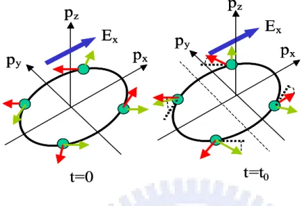
(24) CHAPTER 1. INTRODUCTION. Figure 1.3: The red and green arrows denote the electron spin and momentum, respectively. In the presence of an electric field the Fermi surface (circle) is displaced an amount |eEx t0 /~|at time t0 (shorter than typical scattering times). While moving in momentum space, electrons experience an effective torque which tilts the spin up for py > 0 and down for py < 0, creating a spin current in the y direction.(Phys. Rev. Lett. 92, 126603 (2004)).. 1.5. Motivations. The generation of a spin current becomes one of important goals to carry out the quantum computing processes [44]. To generate spin currents can use Ferromagnetic materials [45, 46], external magnetic field [47, 48], optical-polarized technique [49, 50]. There are several realizable proposals in use of imbalance spin populations to produce the spin currents via magnetic materials (see a review in Ref.[51]). Here, we want to generate and control electron spins in all-electric means in a semiconductor such that the spintronics can be realized through the conventional fabricating processes of the semiconductor. In semiconductors, the great enhancement of SOI provides a novel way to manipulate the electron spin by applying the ac external fields in ballistic and diffusive regimes [21, 23, 52]. Form the insight of conventional charge pumping, we open an inspiration to make spin pump through SOI by time-dependent electric fields in ballistic regime. The ballistic regime, the spin relaxation length lso is much smaller than the mean free path lmean . The conventional charge pumping indicates that a dc charge current can be generated. 10.
(25) CHAPTER 1. INTRODUCTION. Figure 1.4: (A and B) Two-dimensional images of spin density ns and reflectivity R, respectively, for unstrained GaAs sample measured at T=30 K and E=10 mV/µm (Science 306, 1910 (2004)).. 11.
(26) CHAPTER 1. INTRODUCTION by applying two time-dependent field in mesoscopic structures in the adiabatic regime [53, 54]. The non-adiabatic pumping show the time-dependent Bragg reflection mechanism for a time-dependent finger-gate array system.[55] In the first case, either Fermi energy is larger than the oscillating frequency EF À Ω or energy level spacing is larger than the oscillating frequency ∆E À Ω. The latter can release the restriction of oscillating frequency Ω. These above cases involve only the generation of the charge current without the spin-dependent transport. When the semiconductors are incorporated the SOI, the time-dependent fields can induce both of the charge-dependent and spin-dependent transport to pump electron spins. The SO coupling constant can be experimentally tuned up to 50 percentage by modulating the gate voltage [15, 56]. One can expect that the ac-biased gate can cause the SO coupling constant varying with time. Different from adiabatic regime, two independent time-dependent potentials have to be applied in order to generate a spin current [22]. It is a new finding that applying a single ac-biased finger-gate (FG) can generate a dc spin current without charge current in a Rashba-type quantum (RQC) channel [52]. We also found that such a dc spin current can be greatly enhanced by two ac-biased FG structure in the coherent regime. Due to this constrain, the spin relaxation length lso is lager than the coherent length lc such that the spin can not be relaxed during transport. Furthermore, we are also interested in the generation of spin and charge currents by two FG with a finite phase difference. In the ballistic regime, the suppression of spin current generation by backscattering processes is one important issue to examine the generation of a dc spin current via a ac-biased FG. We demonstrate two kinds of elastic scatterers: type (A) is a full static barrier across the RQC and type (B) is a small scatterer located within the RQC. The scatterer of type (B) can be repulsive or attractive one in order to understand the potential dependence of backscattering processes. The robustness of spin current generation against the elastic scattering has been studied [57]. The spin accumulations can be induced by the SHE to become a powerful tool of the spin injection in the diffusive regime. In the diffusive regime, the spin relaxation length 12.
(27) CHAPTER 1. INTRODUCTION is much larger than the mean free path (lso À lmean ). The finite spin-Hall current can be established in a 2DEG with cubic Dresselhaus SOI in the diffusive two-dimensional (2D) strip [42]. The advantage is the all-semiconductors junction and the manipulation of spins in electric means to avoid the conductivity mismatch. Because the spin-Hall current is induced by a driving electric current, the electric current can be influenced due to the feedback of the spin-Hall current [42]. An applied in-plane magnetic field can modulate the symmetric properties of spin accumulations induced by either extrinsic or intrinsic SHE. Several experiments observed the symmetric properties of Sz by varying the in-plane magnetic field B yˆ perpendicular to the electric field E xˆ [36, 59] for the extrinsic SHE. Because the bulk spin polarization is zero for the case of extrinsic SHE, the lowest correlation of the magnetic field By is up to the second order of By . Such that the spin accumulation Sz is even function of By . However, there is a finite bulk spin density associated with Dresselhaus SOI, the spin accumulation can be varied proportional to linear in-plane magnetic field. Our calculation shows that spin density Sz demonstrates the asymmetric property with varying B yˆ for the intrinsic SHE by applying an electric field E xˆ. However, we also show symmetric property of Sz in varying B xˆ in our result. Although the zero spin-Hall current is presented for the case of Rashba SOI, the local spin polarization can be formed a ”spin dipole” around an elastic impurity for both ballistic and diffusive regimes. From Landauer’s dipole concept, the total resistance can be recognized as summing over contribution of each electric dipole induced around each impurity by a driving current. Because the electric current can be correlated by the spinHall current, the nonequilibrium spin dipole around each impurity can be induced by the intrinsic SHE. The spin polarization perpendicular to the two-dimensional electron gas (2DEG) was calculated for the ballistic regime around a scatterer with Rashba SOI [60]. The electric dipole induced around the impurity is parallel to the electric field but the spin dipole induced around the impurity is perpendicular to the electric field. Furthermore, one can utilize spin dipoles created by SOI near macroscopic boundaries 13.
(28) CHAPTER 1. INTRODUCTION and sum over contributions of spin dipoles to obtain the spin accumulation near the macroscopic boundaries. For the case of hard-wall boundary, this finite spin density should be cancelled by the same magnitude but opposite-polarized spin density generated by the boundary surface.. 1.6. A guiding tour to this thesis. In Chapter 2, we investigate the characteristics of a spin-dependent pumping in the lowdimensional system. We propose and demonstrate theoretically that resonant inelastic scattering (RIS) can play an important role in dc spin current generation. The RIS makes it possible to generate dc spin current via a simple gate configuration: a single finger gate that locates atop and orients transversely to a quantum channel in the presence of Rashba spin-orbit interaction. The ac-biased finger gate gives rise to a time variation in the Rashba coupling parameter, which causes spin-resolved RIS and, subsequently, contributes to the dc spin current. The spin current depends on both the static and the dynamic parts in the Rashba coupling parameter. The proposed gate configuration has the added advantage that no dc charge current is generated. Our study also shows that the spin current generation can be enhanced significantly in a double finger-gate configuration. In double finger-gate with the finite phase difference φ, it is also show that the spin current and the charge current are generated by the double ac-biased finger-gate with a finite phase difference φ. We also explore the robustness of such dc spin current generation against elastic scattering in the RQC. The effect of backscattering is studied by introducing two kinds of scattering potentials in the transverse dimension. These two kinds of scattering potentials are divided into type (A): full static barrier and type (B): small scatterer in the transverse dimension of a RQC. The modulations of spin currents depend on the forms of scattering potentials. In Chapter 3, the diffusion equation of spin densities Si (for i =x, y, z) is derived for the intrinsic spin-Hall effect (SHE) due to the spin-orbit interaction (SOI). At the same time,. 14.
(29) CHAPTER 1. INTRODUCTION the diffusion equation of spin currents is also derived and the spin currents are associated with the spin densities. Here, we employ the nonequilibrium Green’s functions to calculate all diffusion equations and take the suitable orders into account. The restrictions of boundary conditions are given by spin currents. In particularly, spin currents turn out to vanish for hard-wall boundaries. In our cases, we consider the hard-wall boundaries in a 2D strip. In Chapter 4, the intrinsic spin Hall effect (SHE) on spin accumulation and electric conductance in a diffusive regime has been studied for a 2D strip with a finite width d. It is found that the spin polarization near the edges of the strip exhibits damped oscillations as a function of the width and strength of the Dresselhaus spin-orbit interaction (SOI) while an electric current is applied in the longitudinal direction. Cubic terms of Dresselhaus SOI are crucial for spin accumulation near the edges. As expected, no effect on the spin accumulation and electric conductance have been found in the case of Rashba SOI. At the same time, the conventional electric current can be correlated by the SHE. This correlation is associated with the magnitude of the spin accumulations on the edges. In Chapter 5, we studied the intrinsic spin-Hall effect (SHE) induced by a driving electric field E xˆ, in the presence of an in-plane magnetic field Bk = Bx xˆ + By yˆ on a 2D strip. In the diffusive regime, the spatial distribution of the spin density Si (i = x, y, z) is calculated from a spin diffusion equation derived from the nonequilibrium Green’s function. In the presence of the in-plane magnetic field, the z-component spin density Sz normal to the 2D strip remains zero with or without Bk field for the case of Rashba spin-orbit interaction (SOI). For the case of Dresselhaus SOI, the spatial distribution of spin density show either symmetric or asymmetric features which depend on the direction of the in-plane magnetic field. By applying the longitudinal magnetic field Bx , the spatial distributions of spin densities Sx and Sz show the even parity in Bx but Sy shows the odd parity in Bx . The asymmetric property of Sz versus By is demonstrated for the intrinsic SHE in case of Dresselhaus SOI. The extrinsic SHE experimentally performed the symmetric behavior of Sz at boundaries by applying in-plane magnetic field By . These 15.
(30) CHAPTER 1. INTRODUCTION robust features of spin densities provide a possible diagnostic tool to identify the intrinsic and extrinsic SHE by applying an in-plane magnetic field. In Chapter 6, the nonequilibrium spin dipoles which are induced around spin-independent elastic scatterers by the intrinsic spin-Hall effect in the two-dimensional electron gas (2DEG) subject to the Rashba spin-orbit interaction. The spin polarization normal to the 2DEG can be calculated in the diffusive regime around the elastic scatterer. It is found that there is the finite spin polarization around each impurity. However, the macroscopic spin density turns out to vanish by averaging of individual spin dipole distribution over impurities for a hard wall boundary. At the same time, the spin density is finite near the boundary of 2DEG for a soft-wall boundary. Finally, we present our conclusion and future works in Chapter 7.. 16.
(31) Chapter 2 Dc spin current generation in a Rashba-type ballistic quantum channel In this chapter, we investigate the characteristics of a spin-dependent pumping in the low-dimensional system. We propose and demonstrate theoretically that resonant inelastic scattering (RIS) can play an important role in dc spin current generation. The RIS makes it possible to generate dc spin current via a simple gate configuration: a single finger gate that locates atop and orients transversely to a quantum channel in the presence of Rashba spin-orbit interaction. The ac-biased finger gate gives rise to a time variation in the Rashba coupling parameter, which causes spin-resolved RIS and, subsequently, contributes to the dc spin current. The spin current depends on both the static and the dynamic parts in the Rashba coupling parameter, α0 and α1 , respectively, and is proportional to α0 α12 . The proposed gate configuration has the added advantage that no dc charge current (CC) is generated. Our study also shows that the spin current generation can be enhanced significantly in a double finger-gate configuration. In a double finger-gate with a finite phase difference φ, it is also show that the spin current and the CC are generated by a double ac-biased finger-gate with a finite phase difference φ. We. 17.
(32) CHAPTER 2. DC SPIN CURRENT GENERATION IN A RASHBA-TYPE BALLISTIC QUANTUM CHANNEL also explore the robustness of such dc spin current generation against elastic scattering in the RQC. The effect of backscattering is studied by introducing a static barrier (type A) that is uniform in the transverse dimension. The effects of both backscattering and subband mixing is studied by introducing a static partial-barrier (type B) that is spatially localized and non-uniform in the transverse dimension. In addition, we compare the cases of attractive and repulsive partial-barriers. It is found that attractive partial-barrier gives rise to additional DC spin current structures due to resonant inter-subband and inter-sideband transition to quasi-bound states formed just beneath subband thresholds.. 2.1. Introduction. Quantum charge pumping (QPC) has attracted a lot of interest in recent years [61– 64]. The dc CC can be generated across an unbiased mesoscopic structure by timedependent periodic deformation of two structure parameters. Original proposal of QCP, was suggested [53, 54] in the adiabatic regime. They considered the current generated by a slowly varying travelling wave in an isolated one-dimensional system. The number of electrons transported per period was found to be quantized if the Fermi energy lies in the gap of the spectrum of the instantaneous Hamiltonian. This quantized charge pumping has great potential for the direct-current standard [65]. The requirement of the adiabatic pumping is either the Fermi energy εF À Ω in a continuum mesoscopic system (ex: quantum wires) or the discrete level spacing ∆E À Ω in the quantized system (ex: quantum dots), where Ω is the oscillating frequency. In above cases, the frequency Ω of a time-modulation structure parameters is restricted to be much smaller than an energy scalar in the considered system such that the charge evolves with time adiabatically. Beyond the regime of adiabatic QPC, the non-adiabatic QCP becomes applicable and interesting in a quantum system without strict restriction of Ω. The non-adiabatic pumping show the time-dependent Bragg reflection mechanism for a timedependent finger-gate array system [55]. The charge evolution has to be treated quantum-. 18.
(33) CHAPTER 2. DC SPIN CURRENT GENERATION IN A RASHBA-TYPE BALLISTIC QUANTUM CHANNEL mechanically in non-adiabatic QCP respecting to the semiclassical adiabatic QCP. More recently, the spintronics has become an emerging field because of in both application and foundation arenas [1, 32, 44, 66]. The recent key issue of great interest is the generation of dc spin current (SC) without charge current. Various dc SC generation schemes have been proposed, involving static magnetic field [67–69], ferromagnetic material [70], or ac magnetic field [47]. More recently, Rashba-type spin-orbit interaction (SOI) in two dimension electron gas (2DEG) [12, 15, 56] has inspired attractive proposals for nonmagnetic dc SC generation [22, 23, 71]. Of these recent proposals, including a time-modulated quantum dot with a static spin-orbit coupling [71], and time modulations of a barrier and the spin-orbit coupling parameter in two spatially separated regions [22], the working principle is basically adiabatic quantum pumping. Hence, simultaneous generation of both dc spin and charge current is the norm. The condition of zero dc CC, however, is met only for some judicious choices for the values of the system parameters. It is known, on the other hand, that quantum transport in a narrow channel exhibits resonant inelastic scattering (RIS) features when it is acted upon by a spatially localized time-modulated potential [72, 73]. This RIS is coherent inelastic scattering, but with resonance at work, when the traversing electrons can make transitions to their subband threshold by emitting m~Ω [72, 73]. Should this RIS become spin resolved in a Rashbatype quantum channel (RQC), of which its Rashba coupling parameter is time modulated locally, we will have a simpler route to the nonmagnetic generation of dc SC. Thus, we opt to study, in this work, the RIS features in a RQC. This requires us to go beyond the adiabatic regime and into the regime when either µ or µn ∼ ~Ω. We solve the time-dependent spin-orbit scattering (SOS) for all possible incident electron energies and obtain large RIS contribution. In the adiabatic regime, however, with µ, µn À ~Ω, we find that the dc spin-pumping effect from a sole SOI time-modulated region is small [22]. The system configuration considered is based on a RQC that forms out of a 2DEG in an asymmetric quantum well by the split-gate technique. As is depicted in Fig. 2.1 (a), a finger gate (FG) is positioned above while separated from the RQC by an insulating 19.
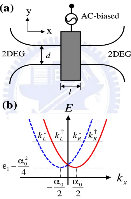
(34) CHAPTER 2. DC SPIN CURRENT GENERATION IN A RASHBA-TYPE BALLISTIC QUANTUM CHANNEL. (a). y. AC-biased. x 2DEG. 2DEG. d. l. (b). E k L↓ k L↑. α 02 ε1 − 4. k R↓ k R↑. α0 2. α0 − 2. kx. Figure 2.1: (a) Top-view schematic illustration of the RQC. The ac-biased FG, of width l , is indicated by the gray area; (b) the electron dispersion relation of an unperturbed RQC.. 20.
(35) CHAPTER 2. DC SPIN CURRENT GENERATION IN A RASHBA-TYPE BALLISTIC QUANTUM CHANNEL layer. A local time variation in the Rashba coupling parameter α(r, t) can be induced by ac biasing the FG [22, 23]. The Hamiltonian is given by H = p2 /2m + Hso (r, t) + Vc (y) where the Rashba term 1 Hso (r, t) = M · [α(r, t)p + pα(r, t)]. 2. (2.1). Here, M = ˆ z × σ is normal to the 2DEG, σ is the vector of Pauli spin matrices, and Vc (y) is the confinement potential. The unperturbed Rashba coupling parameter α(r, t) is α0 throughout the RQC, but becomes α0 + α1 cos(Ωt) in the region underneath the ac-biased FG. In principle, the time-modulating potential can also modulate the electron density but one can applying a backgate to compensate the fluctuation of electron density [56]. The Dresselhaus term is neglected for the case of a narrow-gap semiconductor system [74]. We also investigate the effect of elastic scattering on the dc SC generation in a single FG configuration. The method of approach is time-dependent scattering matrix method [52, 75] with a static potential V (x, y) in a RQC. The backscattering effect can be studied via a static full-barrier locating either inside or outside of the AC-biased FG. Strong barrier position-dependent effect on the dc SC generation is found in our theoretical calculation. The elastic scattering effect is further studied by considering a repulsive or attractive partial-barrier. The partial-barrier introduces intersubband scattering to the system due to the fact that it covers only part of the transverse dimension of the quantum channel. We have studied the barrier position dependence of the dc SC generation. For an attractive partial-barrier, the intersubband transition into a quasi-bound state formed just beneath the subband bottom causes the SC to have an additional structure at m below the second subband bottom. In all the above elastic scattering effect on the dc SC, as long as the barrier breaks the longitudinal symmetry of the configuration, the CC will become nonzero.. 21.
(36) CHAPTER 2. DC SPIN CURRENT GENERATION IN A RASHBA-TYPE BALLISTIC QUANTUM CHANNEL. 2.2. The generation of a spin current via ac-biased FG in the RQC. To demonstrate the pumping mechanism, we consider a narrow RQC in which its subband energy spacing is much greater than the Rashba-induced subband mixing. As such, the unperturbed Hamiltonian, in its dimensionless form, is H0 = −∇2 + α0 σy (i∂/∂x) + Vc (y). Appropriate units have been used such that all physical quantities presented here, and henceforth, are dimensionless. In particular, α is in unit of vF∗ /2 , and spin in unit of ~/2. The right-going (R) eigenstate of H0 , in the nth subband, is φn (y)ψnσ (x), where √ σ σ ψnσ (x) = exp[iknR (x)]χσ . The wave vector knR = µn + ησ α0 /2, while ησ = ±1 denotes the eigenvalue of χσ to the operator σy . µn is the energy measured from the nth subband threshold such that the energy of the eigentstate is E = µn + εn − α02 /4, for εn = (nπ/d)2 . This dispersion relation is shown in Fig. 2.1 (b). The subband with µn ∼ ~Ω is found to contribute most to the RIS-enhanced spin pumping. It is of import to note that right↑(↓). ↑ ↓ going electrons have |kR | > |kR | and that, at the subband threshold kR. ↑(↓). = kL .. The physical origin of the dc SC generation can be understood from two perspectives. A weak pumping regime result is then obtained for an explicit confirmation of our physical reasoning. The first perspective is associated with the vector potential. In the ac-biased region, H = Hx + Hy , the transverse part Hy = −∂ 2 /∂y 2 + Vc (y), and the longitudinal part µ Hx (t) =. α(x, t) ∂ M · xˆ + −i ∂x 2. ¶2 −. α(x, t)2 4. (2.2). ˆ, which The form of Eq. (2.2) suggests an effective vector potential, A(t) = 21 α(x, t)M · x depends on the spin and gives rise to a spin-resolved driving electric field E = −∂A/∂t. However, in Hx , the A2 term does not depend on σ, while for the term linear in A, Aχσ = − 21 ησ α(x, t)χσ gives rise only to a trivial spin dependence, which can be easily removed by a shift in the origin of time for the case of an oscillatory α(x, t). Yet it. 22.
(37) CHAPTER 2. DC SPIN CURRENT GENERATION IN A RASHBA-TYPE BALLISTIC QUANTUM CHANNEL turns out that the full term linear in A, given by −i(∂/∂x)ˆ x · A, manages to give rise to nontrivial spin-resolved transmissions. By the perturbation concept, this term becomes ↑(↓). kR Ax, for the case of a right-going electron incident upon a spatially uniform α(t). This renders the effective longitudinal driving field to become spin dependent, through ↑(↓). the factor kR . The difference in the current transmissions, for spin-up and spin down ↑(↓). cases, is proportional to the difference in kR , or α0 , and is found to be amplified by RIS. This breaking of the longitudinal symmetry in the effective driving field by α0 leads to the generation of dc spin current in a FG-RQC structure that has but an apparent longitudinal configuration symmetry, and with zero source-drain bias. No dc CC will be generated, however, in such a structure. An alternate perspective for the understanding of the origin of the spin-resolved current transmission is associated with unitary transformation. By introducing the unitary Rx transformation Ψσ (x, t) = exp[(iησ /2) −l/2 α (x0 , t) dx0 ]ψσ (x, t), the Schr¨ odinger equation [Eq. (2.2)] becomes ·. ¸ ∂2 ∂ σ − 2 + U1 (t) + U2 (t) ψσ (x, t) = i ψσ (x, t) ∂x ∂t. (2.3). of which the two time-dependent potentials are U1 (t) = −α(x, t)2 /4 and U2σ (t) = (Ωα1 /2)(x+ l/2)cos(Ωt/ + ησ π/2). Even though only U2σ depends on spin, both the term in U1 (t) that oscillates with frequency Ω and U2σ together constitute a pair of quantum pumping potential that pump SC. This is our major finding in this work: that spin pumping nature is built-in even in a single FG configuration. Next, we can write down the total wave functions in the different region for the one-FG configuration in Fig. 2.2. For convenience, the region of the ac-biased FG is located from x = −l/2 to x = l/2 and the channel width is d. The Appendix A shows the derivation of x-dependent wave function in the region (II) via a transformation ∂ )ψσ (x, t). The wave function Ψσ satisfies Hx (t)Ψσ (x, t) = Ψσ (x, t) = exp(ησ αΩ1 sin (Ωt) ∂x. i∂Ψσ (x, t)/∂t and one can rewrite the wave function in the Bessel’s function form. The. 23.
(38) CHAPTER 2. DC SPIN CURRENT GENERATION IN A RASHBA-TYPE BALLISTIC QUANTUM CHANNEL right-going scattering wave functions in regions (I) are consisted of the incident and reflection waves. The right-going scattering wave functions in regions (III) is consisted of the transmission waves. The reflection and transmission wave functions are involved the inelastic and spin-dependent scattering processes due to the time-modulation FG in region (II). In summary, we can express the scattering wave function in x direction as following. m,σ P m,σ σ (I) Ψσ (x, t) = eikn,R x eiµ0 t + rn,LL (m)eikn,L x eiµm t , f or x < −l/2 m ´ ³ m0 ,σ P 0 ,σ (II) m−m0 ikn,R x α1 m0 ,σ 0 0 Ψσ (x, t) = k (ησ ) {Am (m ) e J m−m n,RL ω n,R m,m0 ´ ³ m0 ,σ m0 ,σ m0 ,σ ikn,L x 0 }e−iµm t f or − l/2 < x < l/2 +B (m ) e Jm−m0 αω1 kn,L n,LL P m,σ ikm,σ x iµm t (III) tn,RL e n,R e Ψσ (x, t) = f or x > l/2.. (2.4). m. 0. m ,σ 1/2 Here the wave vector kn,R(L) = ±(µm + ησ α0 /2, with upper (lower) sign corresponds n ) 0. to the right-(left-) moving electron in the nth subband, m0 th sideband, and with kinetic m,σ energy µm n . The reflection amplitude rn,LL indicates that an incident electron is injected 0. from the left-hand side and scattered into the left-hand side with energy µm n in region (I). The transmission amplitude tm,σ n,RL indicates that an incident electron is injected from the left-hand side and scattered into the right-hand side with energy µm n in region (III). The 0. 0. m ,σ ,σ coefficients Am n,RL and Bn,LL corresponding to the amplitude of right-going and left-going 0. wave functions have an energy µm n and the spin state σ in the region (II), respectively. Furthermore, the total scattering wave functions can be written as Ψσ (x, t)ϕn (y), where p ϕn (y) = 2/dsin(nπy/d) is the nth subband wave function for the hard-wall confinement with the channel width d. Our aim is to solve the reflection and transmission coefficients by the imposed boundary conditions: (i) wave functions continuous at x = ±l/2 and (ii) the slope of wave functions are continuous at x = ±l/2. For continuity of wave functions, the Eq. (2.4). 24.
(39) CHAPTER 2. DC SPIN CURRENT GENERATION IN A RASHBA-TYPE BALLISTIC QUANTUM CHANNEL. FG (I). (II). (III). x= −l/2. x= l/2. Figure 2.2: The wave functions can be separated by three different regions (I)(x < −l/2), (II) (−l/2 < x < l/2), and (III) (x > l/2). The region (II) includes the static and dynamic Rashba spin-orbit coupling constant.. satisfy (II) Ψ(I) (x = −l/2, t) σ (x = −l/2, t) = Ψσ (III) Ψ(II) (x = l/2, t) = Ψσ (x = l/2, t) σ. .. (2.5). For the continuity of the wave function’s slope, the Eq. (2.4) satisfy ¯ ¯ ∂ ¯ − ∂ Ψσ ¯ + − 2i ησ α1 cos (Ωt) Ψσ |x=− l = 0 Ψ l σ ∂x ∂x x=− 2 x=− 2l 2 . ¯ ¯ − ∂ Ψσ ¯ l + ∂ Ψσ ¯ l + i ησ α1 cos (Ωt) Ψσ |x= l = 0. ∂x ∂x 2 x= x= 2. (2.6). 2. 2. Essentially, all unknown variables can be calculated from Eqs. (2.5) and (2.6) by cutting off the large enough sideband index m (m0 ) in the exactly numerical sense. (Appendix B) The charge transport generates a CC and the spin transport generates a spin current (SC). The CC is a good physical quantity due to the conservation of the total charges. However, the spin current is not conserved due to the flip of spin during the scattering processes. In our case, the SC conservation is maintained by the suppression of subband mixing and the associated spin-flipping in a RQC. The SC expression for a state Ψσ is. 25.
(40) CHAPTER 2. DC SPIN CURRENT GENERATION IN A RASHBA-TYPE BALLISTIC QUANTUM CHANNEL given by the spin density operator ¸ · † ˆjxy = i ∂Ψσ σy Ψσ − H.c. + α Ψ†σ {σy , M} Ψσ . x ∂x 2. (2.7). The density operator ˆjxy describes the electron moving along x-direction with the ycomponent spin polarization. For a scattering state Ψσ , the SC can be expressed in terms of the transmission coefficients. More specifically, the ratio between the time-averaged σ transmitted and the incident SC gives the spin-resolved current transmission Tβα , where α,. β, are, respectively, the incident and the transmitting lead. Summing over contributions from all states in reservoirs R and L, the SC is I s = I ↑ − I ↓,. (2.8). where Z σ. I =. σ σ dEf (E) [TRL − TLR ]. (2.9). and I σ is the number current due to electrons with spin from both reservoirs that are P P m,σ σ under zero source-drain bias condition. Here TRL = n m(µm Tn,RL and f (E) is the n >0) ¯ ¯2 p m,σ ¯ µm = ¯tm,σ Fermi-Dirac distribution. The transmission coefficient Tn,RL n /µn denotes n,RL the current transmission that an electron incident from terminal L in the spin channel σ, subband n, energy E, is scattered into terminal R, sideband m, with kinetic energy ¯ m,σ ¯2 p m,σ ¯ ¯ µm µm n /µn . The n = µn + mΩ. The reflection coefficient is calculated by Rn,LL = rn,LL −σ σ net CC is given by I c = I ↑ +I ↓ . In a symmetric FG configuration, we have TLR = T=RL , so ³ ´ R ↑ ↓ that the net spin current is I s = 2 dEf (E) TRL − TRL and the net CC is identically. zero. Our numerical results have to check the conservation of the particle flux to satisfy with X ¡. ¢ m,σ m,σ Tn,RL + Rn,RL =1. (2.10). m(µm n >0). 26.
(41) CHAPTER 2. DC SPIN CURRENT GENERATION IN A RASHBA-TYPE BALLISTIC QUANTUM CHANNEL for the nth subband.. 2.3. One-sideband approximation of the single ac-biased FG in the weak pumping regime. For the case of a single ac-biased FG, we can employ the one-sideband approximation m,σ to estimate the transmission coefficient Tn,RL(LR) with m = 0, ±1, and the SC in the. weak pumping (WP) regime. In the WP regime, when α1 is small, we can demonstrate analytically, and most unequivocally, that spin-dependent reflection arises merely from the aforementioned linear A term in Hx (t). We outline the derivation here while leaving the detail in Appendix C. Tracing up to the first order in α1 , our derivation retains the reflection amplitudes to m = ±1 sideband and drops that to the m = 0 sideband. Contribution to the total reflection includes thus reflection at either the left or the right edges of the time-modulated region. For an electron incident from terminal L with wave vecσ tor kn,R (E), the reflection at the left edge is obtained from the wave-function continuous. condition and the boundary condition ¯ ¯ ¯ ¯ ∂ (II) ¯¯ i ∂ (I) ¯¯ (II) ¯ + + ησ α1 cosΩtΨσ ¯ =0 − Ψσ ¯ Ψσ ¯ ∂x ∂x 2 x=−( l )+ x=−( l )− x=− l 2. 2. (2.11). 2. In the time-modulated region, the wave function Ψσ consists of one-sideband terms, given £ ¡ ¢¤ σ σ σ by the form eikn,R (E±Ω)x e−i(E±Ω)t , and eikn,R (E)x e−iEt 1 + ησ / (2Ω) α1 kn,R (E) eiΩt − e−iΩt is given by m = 0 term. The extra Ωt dependence in the m = 0 term is resulted from the time-dependent driving effect of A, which is obviated by the weighting factor that σ involves α1 kn,R . The reflection amplitude rLm,σ , at the left edge is obtained. rLm,σ. £ σ m,σ σ (kn,R − kn,R )+ ησ α1 kn,R = sgn(m) m,σ m,σ 2 kn,R − kn,L m,σ σ ×e−i(kn,R −kn,L )l/2. 27. mα1 2. ¤. (2.12).
(42) CHAPTER 2. DC SPIN CURRENT GENERATION IN A RASHBA-TYPE BALLISTIC QUANTUM CHANNEL for m= 1. The first term in the numerator of Eq. (2.12) is clearly due to A, because of σ the factor α1 kn,R , and the second term is due to the scattering at the edge. Here the wave m,σ 1/2 vector kn,R(L) = ±(µm + ησ α0 /2, with upper (lower) sign corresponds to the rightn). (left-) moving electron in the nth subband, mth sideband, and with kinetic energy µm n. It is clear then that wave-vector differences in both the numerator and the denominator σ of rLm,σ , are spin independent. Hence, the spin dependence arises solely from the α1 kn,R. factor in the first term of the numerator in Eq. (2.12), or from A. This confirms our understanding of the physical origin of the dc SC generation. Including the reflection at the right edge, we obtain the total reflection amplitude m,σ rn,LL. h i σ −k m,σ )l i(kn,R n,L = 1−e rLm,σ. (2.13). We note that the spin dependence of this total reflection amplitude is associated with α0 . In fact, it turns out that the SC is proportional to α0 . The SC is related to the σ current transmission, which, within the aforementioned approximation, is given by TRL ≈ ¯ ¯ ¤ P £ 1,σ −1,σ m,σ m,σ ¯2 √ m √ µn / µn . From Eq. (2.9), the energy 1 − n Rn,LL + Rn,LL , where Rn,LL = ¯rn,LL ´ ³ ↓ ↑ s derivative of the zero-temperature SC is given by ∂I /∂E = 2∆TRL = 2 TRL − TRL. from which its explicit expression is given by. s. ∂I = 2α0 α12 ∂E. X X {1 − cos n. m=±1 (µm n >0). £¡√ √ √ ¢ ¤ h¡ 1 ¢2 ¡ 1 − Ω (µn − µn µm µn + µm n l } n)+ 4 √ µn µm n. ¢ m 2 4. i .. (2.14). That this expression diverges when µm n = 0, for m < 0, exhibits the RIS feature unambiguously and also demonstrates the need to go beyond the one-sideband approximation near the RIS condition.. 28.
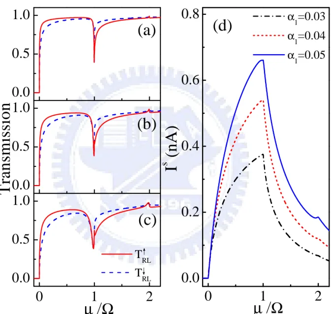
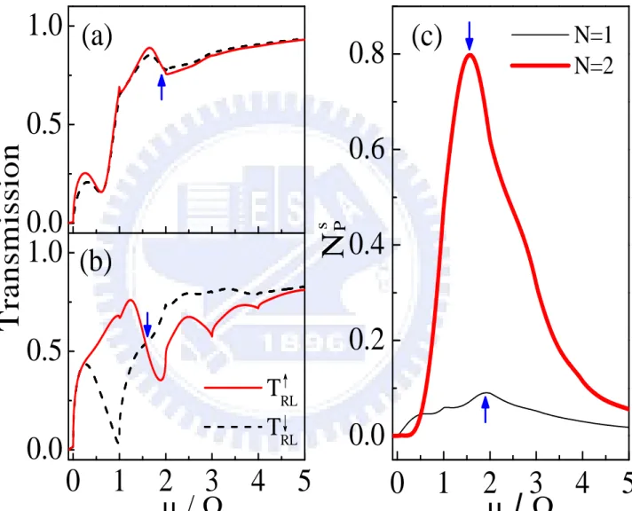
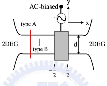
(43) CHAPTER 2. DC SPIN CURRENT GENERATION IN A RASHBA-TYPE BALLISTIC QUANTUM CHANNEL. 2.4. Numerical results for the ac-biased FG in a RQC. In the following, we present results obtained from solving the time-dependent SOS exactly, in the numerical sense. An outline of the method is presented in Appendix B. Physical parameters are chosen to be consistent with the InGaAs-InAlAsVbased narrowgap heterostructures such that the electron density ne = 1 × 1012 cm−2 , effective mass m∗ = 0.04m0 , and α0 = 0.13(~α0 = 3 × 10⁻¹¹ eV m).[56] Accordingly, the length unit l∗ = 4.0nm and the energy unit E ∗ = 59meV . For the case of one FG (N=1), the energy dependence of the spin-resolved transmission sigma TRL is plotted in Figs. Fig. 2.3 (a) - (c), and that of the corresponding dc SC is plotted. in Fig. 2.3 (d). The FG width l = 20 (80 nm), driving frequency Ω = 0.002(ν = Ω/2π ≈ σ 28GHz), and energy µ = E − ε1 . Dip features in TRL at µ/Ω = 1 are the quasi-bound. state (QBS) features, where electrons undergo coherent inelastic scattering to a QBS just beneath its subband bottom [72]. Higher-order QBS features at µ/Ω = 2 are barely shown by the small peaks. Of particular interest is the change in sign in the transmission ↑ ↓ difference ∆TRL = TRL − TRL across the dip structures, namely, ∆TRL (µ = Ω− ) > 0 while. ∆TRL (µ = Ω+ ) < 0. This leads to a nonzero dc SC, peaked at µ/Ω = 1, and is exhibited in Fig. 2.3 (d). It is also shown that the dc SC increases with the oscillating amplitude α1 of the acbiased gate voltage. More importantly, all the above dc SC characteristics, including even their order of magnitudes, are already captured by Eq. (2.14). This lends strong support to our finding that RIS has played a pivotal role in the generation of dc SC. Similar RIS induced peak in Is is found if we vary d instead ofµ. The nonlinear enhancement in the dc SC by two FGs (N=2) is presented in Fig. 2.5(a)-(c). The driving frequency is chosen to be Ω = 0.001(ν ≈ 14GHz), and with l = 22 (≈ 88 nm). For comparison, the N=1 FG transmissions are plotted along with that of the N=2 FG case, in Fig. 2.5 (a) and (b), respectively. The corresponding dc SC, expressed in terms of pumped spins per cycle NPs = (2π/Ω)|I s |, is shown in Fig. 2.5 (c). The pumping is optimized by a choice of the. 29.
(44) CHAPTER 2. DC SPIN CURRENT GENERATION IN A RASHBA-TYPE BALLISTIC QUANTUM CHANNEL. 0.8. 1.0. α1=0.03. (d). (a). α1=0.04 α1=0.05. 0.5. 0.6. (b). 0.4. s. 0.5. I (nA). Transmission. 0.0 1.0. 0.0 1.0. 0.2. (c) 0.5 TRL TRL. 0.0 0. 1. µ /Ω. 0.0 0. 2. 1. µ /Ω. 2. ↑ ↓ Figure 2.3: Spin-resolved current transmissions TRL (red-solid) and TRL (blue-dashed) versus the incident energy µ/Ω. Parameters N =1, α0 =0.13, Ω=0.002, l=20, and α1 =(a) 0.03, (b) 0.04, and (c) 0.05. The corresponding dc SC is plotted in (d).. 30.
數據
![Figure 1.1: Magnetoresistance of three Fe/Cr superlattices at 4.2 K. The current and applied field are along the same [110] axis in the plane of the layers](https://thumb-ap.123doks.com/thumbv2/9libinfo/8266634.172484/16.892.140.743.155.514/figure-magnetoresistance-superlattices-current-applied-field-plane-layers.webp)
+7

Outline
A guiding tour to this thesis
Diffusion equation for spin densities with an in-plane magnetic field
Theory of the spin current in the diffusion regime
Numerical results and discussions
The solutions of spin densities with the in-plane magnetic field for the case
Spin cloud induced by a single impurity
相關文件
Promote project learning, mathematical modeling, and problem-based learning to strengthen the ability to integrate and apply knowledge and skills, and make. calculated
Recycling Techniques are Available to Address Specific Pavement Distress and/or Pavement Structural Requirement.. Introduction to Asphalt Introduction
The nanostructure with anisotropic transmission characteristics on ITO films induced by fs laser can be used for the alignment layer , polarizer and conducting layer in LCD cell.
Using this formalism we derive an exact differential equation for the partition function of two-dimensional gravity as a function of the string coupling constant that governs the
Complete gauge invariant decomposition of the nucleon spin now available in QCD, even at the density level. OAM—Holy grail in
a) Excess charge in a conductor always moves to the surface of the conductor. b) Flux is always perpendicular to the surface. c) If it was not perpendicular, then charges on
• Follow Example 21.5 to calculate the magnitude of the electric field of a single point charge.. Electric-field vector of a
In an Ising spin glass with a large number of spins the number of lowest-energy configurations (ground states) grows exponentially with increasing number of spins.. It is in
