國立交通大學
材料科學與工程系
碩士論文
多孔性低介電奈米群集二氧化矽薄膜結構
與性質關係之探討
Investigation on the Structure-Property Relationship of
Nano-Clustering Silica (NCS) Porous Low-k Thin Films
研 究 生:莊茹媖
指導教授:呂志鵬 博士
多介孔性低電奈米群集二氧化矽薄膜結構與性質關係之探討
Investigation on the Structure-Property Relationship of Nano-Clustering Silica (NCS) Porous Low-k Thin Films
研 究 生: 莊 茹 媖 Student:Shindy Chuang 指導教授: 呂志鵬 教授 Advisor:Dr. Jihperng (Jim) Leu
國 立 交 通 大 學 材 料 科 學 與 工 程 系
碩 士 論 文
A Thesis
Submitted to Department of Material Science and Engineering College of Engineering
National Chiao Tung University In partial Fulfillment of the Requirements
for the Degree of Master
in
Materials Science and Engineering July 2009
Hsinchu, Taiwan, Republic of China
I 多孔性低介電奈米群集二氧化矽薄膜結構與性質關係之探討 研 究 生: 莊 茹 媖 指導教授: 呂志鵬 教授 國立交通大學 材料科學與工程系碩士班
摘 要
本研究探討奈米群集二氧化矽多孔性低介電薄膜(k ~2.8 to 2.0) 由控制母體 TEOS/MTMS 比率以及結構抑制劑(起孔洞劑) TPAOH 之含量對於結構性質之關 係。研究著重在結構之因素,例如:化學以及分子鍵結、孔隙率、孔洞形狀、大 小、以及孔洞之分部。並且探討以上結構因素對於電性、機械性質、以及熱應力 之影響。 NCS2~NCS5 多孔性低介電薄膜具有介電常數介於κ=2.3~2.8。在二氧化矽 (TEOS)之母體內加入了適當的甲基起始物(MTMS)。孔隙率因此隨著 TPAOH 的 增加而提升,NCS2~NCS5 具有孔隙率<27%。因此 NCS2~NCS5 具有 Si-O-Si 很 好的交聯程度而且孔隙率的增加並尚未破壞整個Si-O-Si 交聯的情形,所以最終 還是可達到很好的機械強度(E~10GPa)。孔洞的形貌是為圓形,且具有很窄的孔 洞大小分佈並且孔洞大小皆集中在0.5 nm。 為了更降低 NCS 多孔性低介電薄膜的κ=2.0,因此 NCS1 具有較高的孔隙 率 (38.6%)、Si-O-Si 交聯結構較鬆散、以及具有較低極性 Si-CH3之鍵結,以上 因素皆有利於降低介電常數。NCS1 具有大量的 MTMS (Si-CH3)比起 TEOS (Si-O-Si)。儘管得到最低之 κ 值,相對而言其機械強度也受到損害(E=2.76GPa)。 Si-O-Si 交聯結構較鬆散之母體中具有高孔隙率 38.6%的孔洞,則是高孔隙率以II 及鬆散之母體無法撐住來自加熱過程中之熱應力而倒塌,原先圓形的孔洞也因此 變成橢圓形(din-plane = 3.3 nm dout-of-plane = 1.9 nm)。 總 結 而 言 , 控 制 母 體 的 Si-O-Si 交 聯 程 度 (TEOS/MTMS) 以 及 孔 隙 率 (TPAOH) 是有利於增加最終的機械強度,加入適當的較低極性的 Si-CH3 鍵結 和孔隙率,亦可降低介電常數且不破壞薄膜的機械強度。最後,NCS2 奈米群集 二氧化矽薄膜是具有最好的薄模性質 k=2.3、E=9.2GPa 且有利於將來多孔性低 介電材料薄膜進行銅鑲嵌後段製程整合的主要選擇之一。
III
Investigation on the Structure-Property Relationship of Nano-Clustering Silica (NCS) Porous Low-k Thin Films
Student: Shindy Chuang Advisor: Dr. Jihperng (Jim) Leu
Department of Materials Science and Engineering National Chiao Tung University
Abstract
The structure-property relationship of nano-clustering silica (NCS) porous low-k films (k ~2.8 to 2.0) was investigated by controlling silica matrix TEOS/MTMS ratio and structure directing agent or also acted as pore generator TPAOH concentration. Emphasize had been laid on structure parameters such as the chemical and molecular bonding, porosity, pore size, pore shape and pore size distribution and the influence on ultimate electrical, mechanical, thermal stress properties.
NCS2 to NCS5 porous low-k film have κ-value ranging from κ =2.3 to κ =2.8. The silica matrix was composed by the addition of MTMS (Si-CH3) in balance with TEOS (Si-O-Si). Therefore high modulus porous low-k film was obtained (E~10GPa). NCS2 through NCS5 film possessed spherical pore shape. The accommodation of Si-CH3 was equilibrated by the addition of Si-O precursor, in the agreement that the Si-O-Si linkage of NCS low-k film still preserved in the present of Si-CH3 groups. By adding more TPAOH, the porosity increased from NCS5 to NCS2 (ρ<27%) without causing much deterioration on mechanical modulus. Pore size was well controlled in the order of d<10nm with most population in the d=0.5nm.
IV
that was obtained from less cross-link structure and higher porosity. The silica matrix was composed by higher content of MTMS (Si-CH3) instead of TEOS. Moreover, the incorporation of high methyl content and high porosity ( ρ =38%) to NCS1 significantly reduced the κ value. But the modulus substantially dropped to E=2.76GPa. Nevertheless, its Si-O-Si cross-linking was not rigid enough and also the higher porosity cause matrix could not sustain the thermal stress, therefore collapsed to form more stable structure, and formed elliptic cylindrical pore shape (din-plane=3.3nm dout-of-plane=1.9nm).
Overall, the degree of Si-O-Si cross-link (TEOS/MTMS ratio) and porosity (TPAOH ratio) must be controlled in order to obtain high mechanical modulus NCS film with low dielectric constant. Among these NCS films, NCS2 with k=2.3 and E=9.2 GPa, which possessed optimal ratio of Q [(SiO)4Si] to T [(SiO)3Si(CH3)] group, would be the best ILD candidate materials meeting the requirements of device integration.
V
Acknowledgements
This thesis was carried out in the period from July 2007 until May 2009 at Department of Material Science and Engineering, National Chiao Tung University, under the supervision of Dr. Jihperng (Jim) Leu. This project was financially supported in part by Catalysts & Chemicals Industries Co., Ltd and National Science Council (Taiwan) under Contract No. 96-2221-E-009-216.
First of all, I am very grateful to join Nano-Interconnect & Package (NIP) laboratory. For these years, I am very glad to meet every members of NIP lab. NIP lab has already been my second home during my study in Taiwan. I feel very convenience and happy to be one of NIP member. I am grateful for these experiences, which have certainly influenced my own life in a significant way.
I have to express my gratitude to Dr. Jihperng (Jim) Leu for giving me the chance to manage CCIC Japan project, all kinds of discussion during the project and all priceless helps. I also would like to express my gratitude to Dr. U-Ser Jeng at NSRRC (National Synchrotron Radiation Research Center, Taiwan) for his valuable discussion about GISAXS data analysis.
I would also like to thank the seniors at NIP lab: special thank to Kima Che for his guidance and assistance, special thanks to Yu-Han Chen for his GISAXS discussion, to Kuo-Yuan Hsu for the assistance in TGA, to Hsin-Ling Hsu for every discussions about chemical part. I would like to thank every member of NIP lab for being so friendly. I would like to thank Christine Chiu, Ben Chang, Alan Tu, Gavin Liu, Tai-In Lin, Vincent Hsu, Anthony Wang, Po-Cheng Lai, Yu-Hsiu Ho, Wan-Ding Hsu for the nice office atmosphere and the fellowship at work and during the social events.
Last, but not least, I would like to thank my parents, my sisters and brother for their deep love and encouragement in all situations of my life. Also I would like to thank my boyfriend for supporting me on everything.
VI
Contents
摘 要... I Abstract...III Acknowledgements...V Contents ...VI Table Captions ...X Figure Captions...XI Chapter 1 Introduction ...1 1.1 Background...1Chapter 2 Literature Review...4
2.1 Recent trends in device scaling and interconnect signal delay...4
2.2 Future challenges for ILD materials in interconnect processes...7
2.3 Definition of low-k dielectric material ...8
2.3.1 Definition of dielectric constant...8
2.3.2 Polarization contribution to dielectric constant ...10
2.3.3 Chemical compound and density reduction...11
2.4 Classification of low-k dielectric materials...13
2.4.1 Deposition Method of low-k dielectric materials ...13
2.4.2 The candidate for low-k dielectric materials and related issues. ...15
2.4.2.1 Fluorinated Silicates Glasses (FSG)... 15
VII
2.4.2.3 Carbon-doped oxide (CDO)... 18
2.4.2.4 SiLKTM... 19
2.4.2.5 Porous low-k materials... 20
2.4.2.6 Pure Silica-Zeolite low-k film (PSZ-LK)... 23
2.4.2.7 Nano-Clustering Silica (NCS)... 25
2.5 Structure-property relationship of common porous low-k films ...27
2.6 Properties requirements and challenges in the implementation of low-k dielectrics in the back-end of line...30
Chapter 3 Experimental Section ...33
3.1 Experimental Materials ...33
3.2 Sample preparation...34
3.3 Experimental procedures and flow chart diagram...35
3.4 Characterization Methodologies...37
3.4.1 Fourier Transform Infrared Spectroscopy (FT-IR)...37
3.4.2 Nuclear Magnetic Resonance Spectroscopy (29Si-NMR)...37
3.4.3 X-ray Reflectivity (XRR) ...37
3.4.4 Grazing Incidence Small Angle Scattering X-ray (GISAXS) ...40
3.4.5 Capacitance-Voltage measurement (C-V measurement)...41
3.4.6 Nano-Indenter (N-I) ...42
3.4.7 Bending Beam measurement ...44
3.4.8 Atomic Force Microscope (AFM)... 45
Chapter 4 Results and Discussion...46
VIII
4.2 Structure characterization...47
4.2.1 The impact of silica precursor loading (TEOS/MTMS) on chemical bonding ...47
4.2.2 The impact of silica precursor loading (TEOS/MTMS) on molecular bonding ...50
4.2.3 The impact of TPAOH and TEOS/MTMS loading on density and porosity ...53
4.2.4 The effect of chemical bonding/structure and porosity on film structure...55
4.3 Pore morphology and pore size/distribution characterization ...57
4.3.1 GISAXS Theorem...57
4.3.2 Pore size and pore shape analysis by Kratky-Porod and Guinier Approximation ...60
4.3.3 Pore size, shape, and pore size distribution by GISAXS data fitting analysis and Schultz size distribution ...66
4.4 Mechanisms on the pore formation and pore collapse ...70
4.5 Dielectric Property ...73
4.6 Mechanical Property...74
4.6.1 Mechanical modulus and dielectric constant ...74
4.6.2 The effect of matrix cross-link on mechanical modulus...75
4.6.3 The effect of porosity on mechanical modulus...76
4.6.4 The effect of pore shape on mechanical modulus...78
IX
4.7 Thermo-mechanical property ...84
4.8 Surface roughness analysis...86
4.9 Summary...88
Chapter 5 Conclusions ...92
X
Table Captions
Table 2.1 Polarizability and bond enthalpy of some chemical bonds...12
Table 2.2 Type of ILD materials ...14
Table 2.3 Principle properties of SSQ based dielectric materials (ref)...17
Table 2.4 Commercially available SSQ-based low-k materials (ref)...17
Table 2.5 Key properties of silicon oxide and SiLKTM low-k material. ...19
Table 2.6 Important properties for materials in low-k application ...32
Table 3.1 The compositions of various NCS low-k solutions designated as NCS1 through NCS5 ...34
Table 4.1 Peak position and assignment for each chemical bonding between 700 and 1300 cm-1 (υ-stretching, δ-bending)...47
Table 4.2 Nomenclature, peak assignments and peak positions of 29Si-NMR spectra ...50
Table 4.3 Peak area of Q and T structures for NSC1 through NCS5...52
Table 4.4 Density and porosity of NCS low-k films by using XRR...55
Table 4.5 Pore to pore distance and guinier pore radius estimation for NCS2 to NCS5 NCS low-k films...65
Table 4.6 The fitted parameters from size distribution for NCS2 to NCS5 low-k with spherical shape pores ...68
Table 4.7 Thermal stress range of each NCS porous low-k thin film...86
Table 4.8 Summarize of the properties of NCS low-k films...91
XI
Figure Captions
Figure 2.1 Device scaling projection trend shown in terms of gate length (half pitch) for various microelectronics products. ...4 Figure 2.2 Typical schematic interconnect cross-section with parasitic capacitance
...6 Figure 2.3 Decrease in interconnect delay and improved performance are achieved
by using Cu and low-k dielectric. ...7 Figure 2.4 Historical transition of ITRS low-k roadmap...8 Figure 2.5 Dielectric is placed between two conducting plates, each of area A and
with a separation of d. ...9 Figure 2.6 Variation of dielectric constant with frequency of an alternating electric
field. Electronic, ionic, and orientation polarization contribution to the dielectric constant are indicated...11 Figure 2.7 Basic structure of FSG matrix ...15 Figure 2.8 Depiction of possible bond rearrangements upon SiOF film hydration to produce Si-OH bonding and the release of HF from the film...15 Figure 2.9 Basic structure units of SSQ dielectric materials consist of random,
ladder and cage structures. R= H, CH3 for HSQ and MSQ respectively. ...16 Figure 2.10 Carbon-doped silica glass and schematic bonding structure (a) before
and (b) after cross-linking ...18 Figure 2.12 The conventional formation of porous low-k by using template-type
porogen method. ...22 Figure 2.13 Elastic modulus (E) vesus dielectric constant (κ) for amorphous silicas
XII
and various PSZ ...24
Figure 2.14 Base-catalyzed hydrolysis by nucleophilic displacement ...26
Figure 2.15 Schematics of the nano clustering silica formulation and its film deposition and curing processes. ...27
Figure 2.16 Modulus versus k-value for PECVD SiOC:H low-k film. ...28
Figure 2.17 Elastic modulus as a function of porosity for organo-silicate glass. ...29
Figure 2.18 Logarithmic plots .of relative elastic modulus and relative density for porous films calculated by FEM. ...30
Figure 3.1 The chemical structure of NCS low-k (NCS) precursor (a). tetraethyoxysilane (TEOS) (b). methyltrimethoxysilane (MTMS) (c). tetrapropylammonium hydroxide (TPAOH). ...33
Figure 3.2 Experimental procedure flow-chart diagram...36
Figure 3.3 Definition of the angle of incidence and reflection in an XRR experiment...38
Figure 3.4 Typical geometry of GISAXS measurement...41
Figure 3.5 Film stack of MIS structure for CV measurement ...42
Figure 3.6 Top-view of Al-mask with 3 different dot sizes ...42
Figure 3.7 Schematic plot of a typical load-displacement curve ...43
Figure 3.8 Schematic diagram of our home-built bending beam system ...45
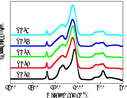
Figure 4.1 Transmission FT-IR spectra of NCS low-k films (NCS1 to NCS5) cured to 400°C in the range 700 cm-1-1500 cm-1...48
Figure 4.2 NCS low-k films Si-O-Si network ratio increased from NCS1 through NCS5...49
Figure 4.3 29Si solid-state NMR spectra of NCS1 to NCS5 samples. ...51
Figure 4.4 The active functional groups in (a) MTMS and (b) TEOS………...….53
XIII
Figure 4.6 Thickness shrinkage during thermal curing process from 150°C to 400°C for NCS1 through NCS5 NCS low-k thin films. ...56 Figure 4.7 GISAXS scattering patterns of NCS low-k films...61 Figure 4.8 Kratky-Porod plot for NCS1 sample with elliptic cylindrical pore shape
...62 Figure 4.9 Guinier plot for NCS2 low-k film spherical pore shape...63 Figure 4.10 Guinier plot in-plane direction for NCS2 through NCS5 low-k films
with spherical pore shape...64 Figure 4.11 Intensity vs. qxy plot to determine the pore to pore correlation distance65 Figure 4.12 NCS1 low-k Intensity versus qxy fitting curve. ...67 Figure 4.13 Intensity vs. qxy fitting curves for NCS2 to NCS5 low-k materials. Black dot lines referred to the fitting lines ...68 Figure 4.14 Pore size distributions of NCS2 to NCS5 low-k with spherical shape
pores ...69 Figure 4.15 Micelle/cluster formation of structure directing agent ...71 Figure 4.16 Illustration of film thickness degradation during thermal curing process.
Matrix Si-O-Si linkage (black spray) and pores (black circle)...72 Figure 4.18 Modulus versus dielectric constant of NCS low-k films...75 Figure 4.20 Modulus of NCS low-k versus porosity. The power law modulus versus
porosity fitting curve was shown in black line. ...78 Figure 4.21 Plots of parameter “B” for equation pore shape related to modulus. ....80 Figure 4.22 Modulus versus dielectric constant for various porous low-k films.
Square and fitting line referred to amorphous silica low-k film, circle referred to experimental NCS low-k film, and triangle referred to pure silica-zeolite low-k film. ...82 Figure 4.23 Prediction on extension of power law modulus versus porosity fraction
XIV
plot. ...84
Figure 4.24 Thermal stresses of NCS low-films on Si-substrate...85
Figure 4.25 AFM image of NCS low-k films. The image size was 1 x 1 μm2. ...87
1
Chapter 1 Introduction
1.1 Background
The downscaling of feature size in integrated circuit has developed in astonishing and remarkable rate. Such pursuit of minimization has exacerbated several difficult challenges, such as RC (Resistance-Capacitance) delay, crosstalk noise and power dissipation. [1] Presently, the utilization of copper (Cu) as a metal conductor combined with low dielectric constant (low-κ) material as an insulator has been a preferable material solution, in addition to other design solutions such as additional metal layers, repeaters, or geometrical trade-off in aspect ratio of metal and dielectric.[2] The original insulator is silicon dioxide (SiO2) with κ= 4.2-3.9. When device dimension is reduced below 250nm, SiO2 insulator is no longer suitable. Therefore, the need of lowering the κ-value of bulk SiO2 can be attained by lowering the density of matrix and/or addition of lower polarizability atoms or bonds. As a result of fervent R&D of low-k material in the past decade, the development of low-κ material yielded fruitful progresses. Organic SiLK (κ=2.65) was first introduced by IBM at 0.13 μm technology node. [ 3 ] However, inorganic dielectric such as carbon-doped oxide (CDO) was adopted by the majority of semiconductor companies mainly in 90nm and beyond. Major commercially available carbon-doped oxide (CDO)s are AuroraTM (κ=2.9, ASM), CoralTM (κ=2.85, Novellus), and Black DiamondTM (κ=2.65-3.0, Applied Materials) [4,5,6].
Since the dense low-κ dielectric has reached its lower limit of κ=2.5 [7]. Inducing porosity in low-κ dielectric material is one possible strategy to achieve κ-value<2.5. [8] Therefore, porous low-k dielectric material is critically needed and has become one of the prominent candidates. Nevertheless, the feasibility of porous low k dielectric film into Cu-interconnect still meets various kinds of integration
2
issues. As reported by Lin et a.l, [9] the CMP feasibility of a low-k material was related to its mechanical properties. Young’s modulus (E) larger than 4 GPa and hardness (H) larger than 0.5 GPa were required to pass conventional CMP. Therefore, the mechanically weak porous low-k dielectric film has become the priority concern. [11, 12] They were particularly prone to damage during processes inducing stress like CMP, assembly, thermal processes and electromigration reliability test. [13, 14, 15] Particularly, porous low-k films were amorphous in nature and exhibited low mechanical modulus, such as porous carbon doped oxide that possessed k~2.3 but has modulus as low as 2.8 GPa, [16, 17] or porous spin on glass that incorporated sacrificial material into amorphous silica matrix also demonstrated low elastic modulus of < 3 GPa with dielectric constant equal to k~2.2. [18, 19].
In recent years, researchers have focused on high mechanical modulus type low-k films such as pure silica-zeolite low-k film. Pure silica-zeolite (PSZ) low-k film offered several potential advantages which including crystalline structure, intrinsically uniform and small pore size over amorphous silica. [20] Typical PSZ has high modulus and low dielectric constant, but the problems such as high surface roughness and high moisture absorption. [21] Therefore, another thrust was to advance the development of silica-zeolite type low-k film with low surface roughness and low moisture absorption by the direct incorporation of hydrophobic methyl groups such as methyltrimethoxysilane (MTMS). Hence, a modified silica-zeolite low-k materials, nano-clustering silica (NCS), was proposed by Catalysts & Chemicals Industries Co., Ltd. [22] NCS has been successfully integrated into 65nm CMOS technology by Fujitsu Ltd. [23,24,25]
The concept of NCS formation was based on zeolite MFI framework structure which yielded high elastic modulus and low dielectric constant. [26] Generally, the NCS was manufactured by hydrolyzing tetraethyl orthosilicate (TEOS) as silica
3
precursor in the existence of tetra-n-propylammonium hydroxide (TPAOH) as structure directing agent (SDA) or pore generator (porogen). In order to emerge the hydrophobicity, the silica precursor was modified by adding the hybrid model of methyltrimethoxysilane (MTMS) as the component of the silica matrix. [17]
The objective of this study was to explore the structure-property relationship of NCS porous low-k thin films. The structures of NCS porous low-k films were manipulated by the ratio of tetraethoxysilane/methyltrimethoxysilane (TEOS/MTMS), which control the matrix formation and hydrophobicity, and an organic structure directing agent, tetrapropylammonium hydroxide (TPAOH) loadings. Hence, the structure parameters which consisted of chemical/molecular bonding, porosity, and pore size/shape/size distribution were first investigated. Their impact on the final properties of NCS porous low-k thin film such as mechanical modulus, dielectric constant, surface roughness and residual stress were also examined. Finally, we make a thorough assessment on the structure-property relationship of NCS low-κ dielectric materials in terms of their applicability in the copper/low-k damascene processing, then make recommendation the best candidate as ILD materials.
1.2 Overview
This thesis is organized into six chapters. Following a brief introduction, Chapter 2 reviews the concepts and needs of low-k material, also accommodate our study motivation and outlook. Chapter 3 presents the experimental methods and instrumentation. Chapter 4 studies the porosity, chemical and molecular bonding environment effects on the ultimate electrical, mechanical and thermo-mechanical properties. Chapter 5 summarizes key results in this study. Chapter 6 presents a few suggestions for future study.
4
Chapter 2 Literature Review
2.1 Recent trends in device scaling and interconnect signal delay
The future of integrated electronics or microelectronics was firstly predicted by Gordon. E Moore in 1965 who projected that: “The number of transistors that can be placed inexpensively on an integrated circuit(IC) has increased exponentially, doubling approximately every two years “, which was also well-known as Moore’s Law. [27, 28] Figure 2.1 shows the trend of various device gate length scaling. [29] Even though it only displays the front-end gate length half-pitch size trend, but it also appropriately can represent the backend interconnect feature size. The scaling itself refers to the continued shrinking in vertical and horizontal directions of chips on the purpose of improve the density (maximum production in a constant silicon area) and device performance (speed and power) under high reliability value.
Figure 2.1 Device scaling projection trend shown in terms of gate length (half pitch) for various microelectronics products.
5
However, the continuous feature size shrinking has brought attention to several interconnect issues, such as resistance capacitance (RC) delay, crosstalk noise and power dissipation. Figure 2.2 shows the typical schematic interconnect cross-section with parasitic capacitance. The size reduction in line and space width of metal enlarges metal line resistance and parasitic capacitance, resulting in serious impact on signal propagation delay and crosstalk noises between metal lines of interconnect. Since one of the major signal delays is associated with interconnect delay, RC delay have become our main concern. Generally, RC delay can be described according to Figure 2.2. By assuming the minimum metal pitch is twice the metal width (W) and the dielectric thickness between the metal lines is the same as the metal height (T), the following equation can be used to predict and calculate the RC delay respectively.[30]
m m Wt L R=
ρ
(2.1)(
)
⎟⎟ ⎠ ⎞ ⎜⎜ ⎝ ⎛ + = + = m m m m V L t W L W t L C C C 2 2ε
(2.2) ⎟⎟ ⎠ ⎞ ⎜⎜ ⎝ ⎛ + = = 2 22 22 m m m t L W L RCρε
τ
(2.3)Where R is the resistivity, Lm is the interconnect line length, W is the interconnect line width, is the permittivity, and tm is the thickness of metal. Continuous scaling down for achieve higher packing density will lead to the size reduction of W and tm, that will induce higher RC delay. Therefore, according to above RC delay approximation equation, proper improvement of RC delay can be achieved by modification of resistivity ( of metal line and relative dielectric constant ( of inter dielectric layer (ILD).
6
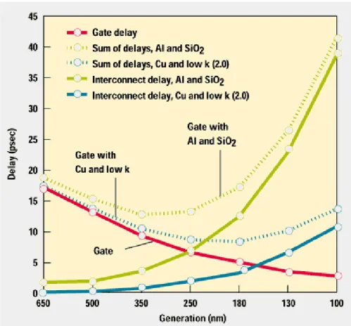
Figure 2.2 Typical schematic interconnect cross-section with parasitic capacitance
In the early dawn of integrated circuit era, the combination of aluminum (Al) alloys with = 2.7 μΩ.cm and silicon dioxide (SiO2) dielectric has been utilized extensively on the interconnect on account of theirs convenient mature subtractive dry-etch processes and the production compatibility with fabricated device which have no performance issues. Even so, the relentlessly ICs marched down toward smaller geometry size in the pursuit of higher integration density and higher speed has even more demanded on material selection integration. Al/SiO2 interconnect system was no longer eligible to fulfill the device geometry shrinkage requirement as shown in Figure 2.3. [1,31] To overcome above mentioned problems, new essential material with low resistivity and low dielectric constant (low-k) for apply as metal line and ILD materials are urgently needed and intensively investigated. Copper (Cu) interconnect are pronounced as one of the most prominent metallization. Possess low resistivity of =1.8 μΩ.cm, Cu-interconnect is widely developed. Lower interconnect delay is gained from Cu/low-k interconnect system compare to Al/SiO2 interconnect
7
system, utilizing copper's 37% lower resistivity than aluminum. [32] However, when technology node has run down to 250nm, the limiting factor of Cu-implementation became obviously observe. The capacitance of interconnect is dominated by line-to-line capacitance. Therefore, a lower dielectric constant material is indeed crucially needed.
Figure 2.3 Decrease in interconnect delay and improved performance are achieved by using Cu and low-k dielectric.
2.2 Future challenges for ILD materials in interconnect processes
In recent years, the back-end ITRS roadmap was re-adjusted year to year as shown in Figure 2.4, the slope displays steeper in ITRS 1999 compare to ITRS 2005 which demonstrating the difficulties and challenges in integrating new types of ILD materials in the Cu-interconnect. The ITRS 1999 projected for 90 nm node k=2.0, but
8
this was later postponed for 32nm node of ITRS 2003. The ITRS stated “Introduction of new materials to….reduce the dielectric permittivity” as one of the key “Five difficult challenges through 2009” for the semiconductor industry. Therefore, low-κ material integration is closely related with the optimization between several tradeoffs, especially material properties, device architectures, and process flows. The principle driving forces for future challenge in integrated low-κ material are lower dielectric constant, minimum process cost and higher process reliability/robustness. The ultimatum for any particular technology node will be resolved by the best compromise among these 3 factors. [35]
Figure 2.4 Historical transition of ITRS low-k roadmap
2.3 Definition of low-k dielectric material
2.3.1 Definition of dielectric constant
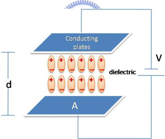
Dielectric constant (κ) (also called relative permittivity (εr)) is defined as the ratio of the permittivity of substance (ε) to that of vacuum (ε0). When an alternating electric field is applied through two plates of capacitor/conducting plate with a
9
medium other than vacuum (Figure 2.5), ex. dielectric substance, the dielectric constant will therefore increase. Generally, capacitance(C) is defined as the ratio of charge ±Q on each conductor to the voltage V between them. Conductor plates area (A), by assuming the distance between those two capacitor plates is d, Thus, finalize the capacitance relationship with dielectric constant can be revealed as
d A d A V Q C = =
ε
=κε
0 (2.4)In which ε0 is the permittivity of vacuum (ε0=8.845.10-12F/m). Consequently, the capacitance is greatest in devices made from materials with a high permittivity.
Figure 2.5 Dielectric is placed between two conducting plates, each of area A and with a separation of d.
10
2.3.2 Polarization contribution to dielectric constant
Any kind of materials containing polar component is represented as dipoles (separation of positive and negative charge in the present of electric field). Dipoles can be characterized by their dipole moment. Many molecules (polar chemical bond) have such dipole moment. From Figure 2.6 which shows the dipoles formation is build up from electronic polarization, ionic polarization and orientation polarization. [36] Electronic polarization is due to the separation of positive charges from negative charges in atoms or molecules of dielectric material due to applied electric field. Ionic polarization occurs in ionic solids whose the dipole moment is disrupted by the application of electric field. Orientation polarization happens in polar dielectric material, which posses permanent electric dipoles. The relationship between polarizability and dielectric constant can be approximately explained by Clausius - Mossotti equation (eq. 2.5) [37] below
[
e e i i dip dip]
r rN
α
N
α
N
α
ε
ε
ε
=
+
+
+
−
03
1
2
1
(2.5)Where is the relative permittivity or dielectric constant, is the electronic polarization, is the number of atoms/ions per unit volume exhibiting electronic polarization, is the effective ionic polarizability per ion pair and is the number of ion pair per unit volume. is the number of permanent electric dipole, and is the dipole orientation polarization.
11
Figure 2.6 Variation of dielectric constant with frequency of an alternating electric field. Electronic, ionic, and orientation polarization contribution to the dielectric constant are indicated.
2.3.3 Chemical compound and density reduction
General bond electronic polarizabilities and related bond enthalpies are listed in Table 2.1. [38] The minimum of polarizability is achieved by single C-C bond. Thereby C-C aliphatic hydrocarbon is being the one of the great potential for low dielectric. Low dielectric might also be obtained by element with small configurational such as smaller atomic radii ex: C-F, C-O and C-H bonds. Conversely, bonding such as C=C double bond or triple bond, need to be avoid, since those bonds have larger polarization due to its increase mobility in π electrons. Although bond enthalpy reveals higher value for double bond and triple bond, which will be an advantages to the higher bond strength compare to single bond. Thus, trade-off stays between lower polarizability that has weaker bond strength while higher bond enthalpy which has higher polarizability.
12
Table 2.1 Polarizability and bond enthalpy of some chemical bonds
Instead of bonding polarity influence on reduction of dielectric constant, the density of low-k film also one of the dramatic concern. To lower the density can be achieved through increasing the free volume by rearranging the material main structure or introducing porosity. In term of porosity itself, can be divided into constitutive or subtractive. Constitutive porosity indicates to the self organization of the material, the porous structure is formed without any additional treatment. Pore size less than 2nm usually observed for constitutive porosity and the porosity is relatively low (<15%). Subtractive porosity involves the addition of thermally degradable substance call porogen. Porogen means pore generator which can induce pores in the material after subsequently removal by an annealing process. Pore size ranging from 2nm to tens of nanometers observes for substractive porosity and the porosity can reach as high as 90%. [39] As a conclusion, organic polymer can combine three approaches. Those include low polarizability bonding, constutive porosity (introduction of free volume) and the use of porogen by subtractive porosity.
13
2.4
Classification of low-k dielectric materials
2.4.1 Deposition Method of low-k dielectric materials
Generally, the major deposition techniques for formation of ILD are divided into primary chemical vapor deposition (CVD) known as “dry” process which has been widely adopted by chip manufacturers and showed highly reliable. The second one knows as “wet” process called spin-on method which has not been greatly developed in the process. There are some trade-off between CVD method and spin-on method. Spin-on process simply involves the coating of liquid/viscous precursor on the substrate before final curing to remove the solvent. It provides planarizing property that shows in a smoother surface which is highly desirable. Compare to CVD method which involves various gases flow and deposit on the substrate, this benefit on cleanliness and minimal waste production. CVD method also provides better conformal coverage of the topography. Table 2.2 listed the CVD and spin-on of various ILD materials with their dielectric constant value. [40]
14
Table 2.2 Type of ILD materials
Material Dielectric constant Deposition method
Low-k materials
Polyimides 3.0-3.6 Spin-on
Spin-on glasses 2.7-3.1 Spin-on Fluorinated polyimides 2.6-2.9 Spin-on DLC (diamond-like carbon) 2.8-3.0 CVD Hydrogen silsesquioxane (HSQ) 2.8-3.0 Spin-on
SILK TM 2.7 Spin-on
Black Diamond TM (SiCOH) 2.7-3.3 CVD Poly(arylene ethers) 2.6-2.9 Spin-on
Poly(arylenes) 2.6-2.8 Spin-on
Methyl silsesquioxane (MSQ) 2.6-2.9 Spin-on
Poly(norbornenes) 2.5-2.7 Spin-on
Fluorinated Parylene 2.5 CVD Polyimide-SSQ hybrids 2.7-3.0 Spin-on
Ultralow k
Teflon microemulsion 1.9-2.1 Spin-on
Porous dielectrics
Polyimide nanofoams 2.2 Spin-on Silica aerogels 1.1-2.2 Spin-on Silica xerogels 1.5-2.2 Spin-on Mesoporous silica 1.9-2.2 Spin-on
15
2.4.2 The candidate for low-k dielectric materials and related issues.
2.4.2.1 Fluorinated Silicates Glasses (FSG)
The first generation of low-k material were fluorinated silicate glasses (FSG) invented by Novellus System Inc. FSG has dielectric constant value as low as k=3.6. FSG posses lower dielectric constant than SiO2 due to incorporation of fluorine into SiO2 matrix film. Fluorine incorporation leads to a less dense, more porous film by creating voids in the SiO2 matrix. Typical FSG film matrix shows in Figure 2.7. Replacing Si–O in the SiO2 matrix with Si–F reduces the polarizability of the matrix. The above reasons contribute to a lower dielectric constant of the FSG dielectric layer. [42, 43] FSG film has some drawback, for instance SiOF film is hydrophobic, in the meantime the fluorine atom will tend to react with hydrogen atom from water absorb in the release of HF moisture when heated to elevate temperature. The moisture of HF will travel along the interface of ILD and metal causing adhesion become poorer as explained by Figure 2.8. [44]
Figure 2.7 Basic structure of FSG matrix
Figure 2.8 Depiction of possible bond rearrangements upon SiOF film hydration to produce Si-OH bonding and the release of HF from the film
16
2.4.2.2 Silsesquioxane (SSQ) based
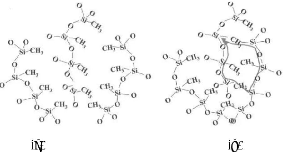
Silsesquioxane (SSQ) based low-k material or commonly called T-resin are organic-inorganic polymer with empirical chemical formula RSiO1.5. The substituents (R) can include hydrogen, alkyl, alkenyl, alkoxy and aryl. The contribution of these organic substituents benefit in lowering the dielectric constant because they provide lower density of the matrix structure. For the addition, they also attributed to less polarizability organic bond (Si-CH3) compare with Si-O bonds in SiO2. SSQ based low-k also known as organosilica glasses (OSG) which yield k=2.7-3.0. The common used SSQ based materials for microelectronic application are mainly hydrogen-silsesquioxane (HSQ) and methyl-silsesquioxane (MSQ). HSQ has hydrogen as a terminal group and MSQ has methyl as a terminal group. The structure of basic units of SSQ shows in Figure 2.9. [45]
Figure 2.9 Basic structure units of SSQ dielectric materials consist of random, ladder and cage structures. R= H, CH3 for HSQ and MSQ respectively.
17
MSQ material has lower dielectric constant compare to HSQ. The contribution of larger –CH3 group that will cause steric hindrance rather than smaller –H group will lower the density of MSQ matrix. The Si-CH3 bond is also a less polarizable bond compare to Si-H. Thus greatly reduce the dielectric constant of MSQ. Table 2.3 summarizes the principle properties of SSQ based dielectric materials compare with SiO2. Subsequently, the commercially available SSQ based low-k materials are summarized in Table 2.4 which has k < 3.0. [46, 47]
Table 2.3 Principle properties of SSQ based dielectric materials (ref)
Property MSQ HSQ SiO2
Dielectric Constant κ 2.8 3.0 4.0
E Modulus (GPa) 3-5 6 59
Density (g/cm3) 1.2-1.3 1.4-1.5 2.4
Tensile Strength σ (MPa) 50 80 -
Table 2.4 Commercially available SSQ-based low-k materials (ref)
Material Trade Name k-value Company
HSQ Fox (flowable oxide) 2.9-3.0 Dow Corning
MSQ RZ25-15 2.6 Hitachi
MSQ HOSP 2.6 Honeywell
Porous HSQ XLK 2.2 Dow Corning Porous HSQ LKD 5109 2.2-2.3 JSR Porous MSQ Zirkon 2.3 Shipley
18
2.4.2.3 Carbon-doped oxide (CDO)
Basically, CDO manage to utilize the chemical vapor deposition (CVD) processing method. CDO low-k is also often designated as SiCOH (carbon-doped silicon oxide). The CDO matrix exists organic bonding such as CH3 backbone that concern lower polarizability in comparison to Si-O as shows in Figure 2.10. Instead of lower polarizability, CH3 also reduce the density of matrix by induced the matrix steric hindrance. Regardless of the precursor used, SiCOH can reach k value in the range of 2.4-3. The k-value depends on the number of CH3 groups build into the structure. The widely studied precursor for SiCOH low-k have been deposited by CVD methods were monometylsilane (1MS), dimethylsilane (2MS), trimethylsilane (3MS), tetra-methylsilane (4MS), Hexamethyldisiloxane, (HMDSO), bis-trimethylsilylmethane (BTMSM), tetravinyltetramethylcyclotetrasiloxane (TVTMCTSO), Vinyltrimethylsilane (VTMS), and tetramethylcyclotetrasiloxane (TMCTS) [48, 49, 50, 51, 52, 53, 54]
CVD CDOs are mainly use in 90nm node. Commercially, the most common CVD OSG materials are AuroraTM (k=2.9, ASM), CoralTM (k=2.85, Novellus), Black DiamondTM (k=2.65-3.0, Applied Materials). [55, 56]
(a) (b)
Figure 2.10 Carbon-doped silica glass and schematic bonding structure (a) before and (b) after cross-linking
19
2.4.2.4 SiLKTM
Spin-coated base SiLKTM was an organic polymer dielectric founded by Dow Chemical in mid 1997. In April 2000, IBM reported the complete integration of SiLKTM dielectric and copper wiring, and announced its intent to commercially fabricate integrated circuits using SiLKTM resin. Toshiba/Sony and Fujitsu also accommodated SiLK resin with hybrid stacks. Aromatic thermosetting polymer SiLKTM with k=2.65 has been proved its compatibility with Cu-dual damascene 0.13 um technology node system. [57] However, the relatively weak mechanical properties of SiLKTM and its poor mismatch of coefficient of thermal expansion (CTE) with copper wires and substrates have prevented a wide adoption of SiLKTM in high-volume semiconductor manufacturing. The comparative properties of SiLK with SiO2 are shown in Table 2.5. [3] Structure repeating unit of organic SiLKTM shows in Figure 2.11. [58]
Table 2.5 Key properties of silicon oxide and SiLKTM low-k material.
Properties SiLKTM Silicon Oxide
Platform Spin-on organic polymer SiO2 Dielectric constant, k 2.65 3.9 Elastic Modulus (GPa) 3 55 to 70 CTE (ppm/oC) 66 to 165 0.45
20
2.4.2.5 Porous low-k materials
The above mentioned low-k materials were all classified into dense low-k materials. In order to reach k<2, fully densified materials has seemingly reached theirs lowest capability. Hence, the research has to move on with introduction of porosity onto the dense materials. There are two type pore formation inside the dense low-k matrix. The primary one is pores that are inherently formed inside the matrix through sol-gel process, ex: aerogel and xerogel low-k film. The secondary one is formed though the template type which accommodate the present of sacrificial materials which are also called “porogen” or pore generator that are decomposed upon the thermal process. Following we will discuss the fact and issue of each porous low-k materials.
1. Silica aerogel and xerogel low-k film
SiO2 aerogel thin film has attracted significant attention because of their unique properties such as ultralow dielectric constant, high porosity, and high thermal stability. SiO2 aerogel thin films usually take the advantage of aging processes. However, SiO2 aerogel thin films usually synthesis above the supercritical pressure (>60 bar) and high temperature of drying solvent process, which is very expensive and hazardous. Thus, it will become constraint for the production in industrial application. [59] Due to their high porosity, SiO2 aerogel thin film have not display superior mechanical properties. [60] SiO2 xerogel thin films also employ the same aging technique as SiO2 aerogel thin film. The differences between aerogel and xerogel is SiO2 xerogel prepared by the ambient drying process which involve pre-drying step that called surface modification process known as silylation. The intention of silylation process is to change the surface hydroxyl (-OH) groups into inert methyl (-CH3) groups. This procedure ensure the film absorb minimal moisture
21
from the environment. [61] Both SiO2 xerogel and aerogel has been reported to reach k-value <2 at porosity level of 70-90%. [ , 62, 63, 64, 65]
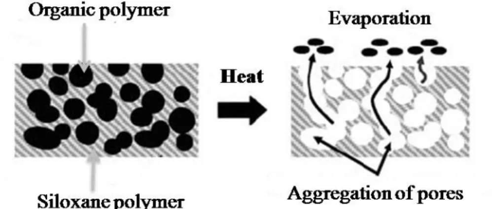
2. Template-type (porogen) low-k films
Furthermore, the incorporation of thermally-labile pore generator also can produce porous SiO2 thin film. The removal of porogen upon high temperature heating will be replaced by pores inside the matrix of SiO2. First method, incorporation of porogen into the SiO2 matrix can be accomplished by simply dispersing or mixing the porogen into the solution of SiO2 precursor. [66, 67, 68] Porogen size determines the final pore size that exists inside the matrix. Percentage of porogen added or also called porogen loading determines degree of porosity inside the final cured matrix. [69, 70] However, during thermal heating process, the random distribution of pores tends to agglomerate and coalescence which cause a burden to the mechanical strength of final SiO2 film especially when the porogen loading is increased as shown in Figure 2.12. [71, 72] The mechanical property of porogen templated low-k film results on lower elastic modulus, the present of porogen in the surrounding of silanol matrix will disturb the condensation of silanol groups (2SiOHÎSi-O-Si+H2O) to form Si-O-Si skeleton. Since Si-O-Si skeleton cross-linking determines the modulus of film, therefore the incorporation of higher porogen loading to obtain lower κ will cause the deterioration of film modulus. [73]. Second method, the porogen is chemically linked or grafted to the SiO2 polymer. [74, 75, 76] This method can achieve better control of porogen distribution in the SiO2 dielectric film. Porogen selection must compatible with SiO2 matrix precursor in order to avoid phase separation. Closely to this theory, phase separation method can be utilized when choosing the suitable porogen.
22
Figure 2.12 The conventional formation of porous low-k by using template-type porogen method.
Recently studies have shown that various organic or inorganic polymer could be applied to form more ordered pore size and pore shape with narrower pore size distribution. Regarding to their ability to self assembly and form micelle when the thermal curing process takes place, block copolymers have become one of the promising candidates for low-k dielectric. Amphibilic di-(or tri-) block copolymer such as PEO-b-PPO-b-PEO [77], PS-b-PEO [78], PS-b-P2VP [79], PS-b-P4VP [42], etc have been studied widely. Various nanoporous low dielectric films have been realized using poly(methyl silsesquioxane) (PMSSQ) as a matrix material with a wide variety of pore generating materials (porogens) such as star-shaped polymers (Polycaprolactone (PCL)) [80, 81, 82], block copolymers [83, 84], cyclodextrines [85, 86, 87], norbornenes [88, 89], dendrimers [90, 91], and hybrid type porogens [92, 93, 94, 95].
Another way to overcome the aggregation issue of porogen is by adopting fast curing and slow curing process [96]. Slow ramp-curing allows porogen diffusion and slow matrix cross-linking. During this curing, porogen percolation leads to form surface agglomerates. Using faster ramp curing, the matrix is cross-linked around porogen nanoparticles faster, and afterward the porogen is degraded at high temperature to leave a network of nanopores in a rigid ULK dielectric matrix.
23
Controlling Curing temperature and ramping rate are important factor for nanoporous ULK dielectrics quality. [96] Moreover, alternative curing process, such as UV, or e-beam assisted thermal cures, would be helpful in providing good film performance. [97, 98] For example, UV radiation could be used to break porogen bonds, leading more easily to their extraction and it also promotes cross-linking that will improve mechanical modulus. [99] The problem that UV-cure meets in the packaging process is the increase in film stress that will cause cracking of film stack and delamination. [100] Therefore, the entire list of the UV cure performance specifications that ultimately determine the quality of the UV cure process must be considered. [101] E-beam assisted thermal cure can improve crosslinking, but it also causes charge damage. [102]
2.4.2.6 Pure Silica-Zeolite low-k film (PSZ-LK)
Pure silica zeolite low-k films (PSZ-LK) have been pronounced as a promising low-k material. A key advantage of PSZ was the ability of decreasing κ value while maintaining much higher mechanical modulus compare to amorphous porous low-k materials. The PSZ has been investigated to possess two film-deposition processes: in situ crystallization and spin-on of a zeolite nanoparticle suspension. [16,103,104, 101,102,103] The in-situ films were pure zeolitic silica films that clearly revealing the intrinsic property of zeolites. The spin-on films were composites of PSZs and amorphous silica which were not totally the intrinsic properties of pure zeolites. Nevertheless the spin-on films have the advantage of obtaining a k-value in the ultralow-k range. Moreover, the spin-on deposition technique was more viable for the manufacturing of integrated circuit. The silica zeolite coating film having the MFI crystalline structure has elastic modulus of 16 to 18 GPa with κ=2.3 [105,106]. The PS-ZLK was developed to take advantage of both the intrinsic zeolite mircoporosity
24
(d=0.55nm) and interparticle mesoporosity (d=2.7-3.3nm). [107] Figure 2.13 depicted the comparison of amorphous silica with PSZ modulus (E) versus dielectric constant (κ) plot. [15,108] It was obvious that PSZ low-k film offered a significantly superior elastic modulus to amorphous silicas at any given k-value.
Figure 2.13 Elastic modulus (E) vesus dielectric constant (κ) for amorphous silicas and various PSZ
The major problem of this high elastic modulus PSZ low-k film was the moisture-absorption was too high. [109, 110] The κ rapidly increased from 2.3 to 3.9. Absorption of moisture could result in significant increase of κ because of water has a very high κ (κ=80-90). This was disadvantageous lost for the practicability of PSZ film. Therefore, there have been some efforts to overcome this problem such as extra post spin-on treatment, by subjecting the PSZ film to silylation (vapor phase silylation
25
using chlorotrimethylsilane (CTMS) or hexamethyldisilazane (HMDS)) to make the surface become more hydrophilic. [111, 112]. Overall, the disadvantages of PSZ low-k film were:
a. Although silylation step was effective, it was considered highly undesirable in semiconductor industry because silylation step was an extra step. It would also increase the manufacturing cost.
b. The silylation step was only hydrophobized the surface of PSZ low-k film. It was also some difficulty for CTMS or HMDS molecules to diffuse into the pore of MFI (micropore=0.55nm). Therefore may have difficulty in assessing the silanol groups inside the micropore. [113] This was inevitably when the PSZ low-k film was subjected to etch or ash process; it would cause the moisture absorption inside the pores and worsen the κ.
c. The size of zeolite particles was around 40-70nm. [114] The surface obtained from zeolite coating film was substantially rough. For instance, further polishing was needed to smooth the surface. This would also increase the manufacturing cost.
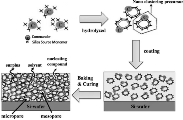
2.4.2.7 Nano-Clustering Silica (NCS)
A novel pore forming method based on spin-on nano-clustering silica (NCS), schematically illustrated in Figure 2.15. [20] The nano-clustering silica, a MFI-type zeolite film was prepared by sol-gel method. NCS precursor prepared by mixing main matrix of silica source tetraethoxysilane (TEOS) as a soldier in the existence of organic structure directing agent such as tetrapropylammonium hydroxide (TPAOH) as a commander in the present of appropriate solvent such as ethanol. The hydrophobicity of the surface of precursor was modified by adding alkoxysilane (AS) such as methyltrimethoxysilane (MTMS) as a component of the matrix. The
26
difference between pure zeolite low-k and NCS is the addition of methyl (-CH3) groups directly into the precursor.
The sol-gel preparation composed of two steps: 1. The hydrolysis of TEOS and MTMS
Si(OC2H5)4 + H2O → (C2H5O)3Si-OH+C2H5OH H3CSi(OCH3)3+ H2O → (CH3O)2Si-OH+CH3OH 2. Water Condensation reaction
(C2H5O)3Si-OH+ (C2H5O)3Si-OH→(C2H5O)3Si-O-Si(OC2H5)3+H2O (C2H5O)3Si-OH+(CH3O)2Si-OH→(C2H5O)3Si-O-Si(OCH3)2+H2O 3. Alcohol Condensation
(C2H5O)3Si-OC2H5+HO-Si(OC2H5)3→(C2H5O)3Si-O-Si-(OC2H5)3+C2H5OH
Water and ethanol were produced by the formation of siloxane (Si-O-Si) bonding. To avoid the formation of striation in the spin-on films due to low boiling point solvents present in the suspension ex: water, ethanol, and methanol. Therefore, solvent substitute processes were followed after sol-gel process by replacing with propylene glycol monomethyl ether (PGME) and propylene glycol monopropyl ether (PGP).The addition of aqueous TPA+OH- would promote the hydrolysis of TEOS due to nucleophilic displacement reaction (SN2-type mechanism) as following mentioned [115]
27
Figure 2.15 Schematics of the nano clustering silica formulation and its film deposition and curing processes.
2.5 Structure-property relationship of common porous low-k films
From above reviewed, porous low-k material was obtained through the incorporation of pores into the dense matrix. Generally the incorporation of pores would sacrifice the elastic modulus of the porous low-k film. The most common PECVD deposited carbon doped oxide film has κ= 3~2.5 with modulus higher than 10GPa, along with the incorporation of 35% porosity, the modulus was largely dropped to 2.8GPa if the porogen was removed through furnace curing. Nevertheless, the low modulus of furnace curing could be improved through e-beam treatment which could increase the modulus to 5.8 GPa with κ= 2.3. The modulus of was improved due to higher network/cage ratio of e-beam treated film compared to furnace cured. [116] From theoretical investigation also revealed the same behavior, higher crosslink of hydrocarbon components instead of terminal methyl groups (-CH3 group) would improved the mechanical strength without adversely affecting the small
28
dielectric constant. [117] The incorporation of more methyl groups was beneficially in reducing the dielectric constant since by replacing the Si-O by Si-CHn bonds would also increasing the porosity, as Si-CHn bonds could generate voids. The nano-voids formed due to the steric hindrance offered by Si-CHn bonds. [118, 119] As the porosity of porous SiOC:H films increase approximately 30-60%, the modulus decreased from approximately 5 GPa with κ~2.4 to 1 GPa. With κ~2.0 as shown in figure 2.16 [120]
Figure 2.16 Modulus versus k-value for PECVD SiOC:H low-k film.
For a given porogen, increasing the volume fraction from ~10% to ~40% depresses the value of k from 2.7 to 2.0, with a corresponding increase of the pore size. The mechanical improvement with UV-assisted curing was then mainly related to chemical changes in the skeleton. Porous film containing large voids were observed at the porogen loading between 20% and 30%. This transition represents percolation threshold of the cavities when they were becoming fully interconnected.[121] If the porosity is increased to above ~25-30% the pores will percolate (coalesce together to
29
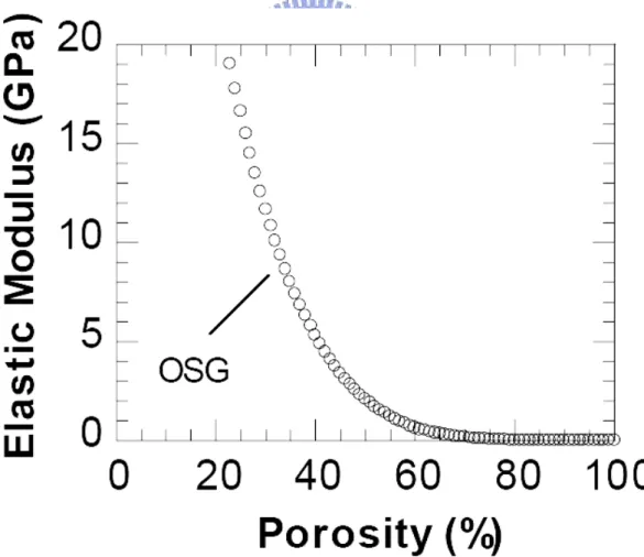
form interconnected pores). The pore diameter also tends to increase with increasing porosity, and the pore size distribution may increase. Higher porosity, interconnected pores, and a large pore size distribution all degrade mechanical strength. The empirical elastic modulus versus porosity for organo-silicate glass (OSG) relationship could be predicted by percolation theory as shown in Figure 2.17.[122] Increasing the carbon doping further reduces strength by lowering the density of strong Si-O bonds. Dense oxide was a network of tetrahedral Si-O bonding, and introducing Si-CH3 bonds resulted in domains with only two or three Si-O bonds instead of four. Thus the ability to control the film structure at a molecular level would allow the maximum possible mechanical strength at a given κ-value. [123, 124]
30
From FEM results, an empirical formula, which describes the relation between density and elastic modulus for porous films as a function of pore aggregation, can be obtained. As shown in Figure 2.18, logarithmic values of elastic modulus linearly depend on logarithmic values of density of porous films calculated for ordered pore structure and random pore structure. [125]
Figure 2.18 Logarithmic plots .of relative elastic modulus and relative density for porous films calculated by FEM.
2.6 Properties requirements and challenges in the implementation of
low-k dielectrics in the back-end of line
ILD materials which well known as low-k materials were used in the replacement of conventional SiO2 in the multilayered microelectronic structure. The application must agree with the processing and packaging conditions. Therefore, several important properties are needed to be focused on, as listed in Table 2.6. The thermal stability must able to withstand the elevate temperature processing of copper metallization that occur at 250°C and usually followed by thermal annealing in the
31
range of 400°C-450°C to ensure the void free copper deposition. Therefore, during this thermal curing, the thermal mismatch issue between Cu and ILD also cannot be neglected. Coefficient of thermal expansion (CTE) of Cu is 16.5ppm/°C, and SiO2’s CTE is 0.5ppm/°C which is relevant to each other.[126] However, new ILD materials mostly consist of organic dielectric have high CTE in the range of 50ppm/°C which is not prefer in the processing since it might cause thermal mismatch and highly stress that might also cause reliability issue.
Mechanically, the low-k layers must be strong enough to endure the chemical mechanical polishing (CMP) process. The young’s modulus, hardness must be high enough to prevent cracking or delamination. The lowest young’s modulus which can pass the CMP process is 5GPa and hardness larger than 0.5GPa. [127, 128] The chemical resistance must also agree with the requirement, hydrophobic surface which can result on low moisture absorption.
Another advance in development of low-k materials can be obtained by inherent pores into the system. Since kair =1, thus it is benefit to lower the k-value. The structural problematic is also required. Pores with small size, closed shape, no interconnect geometry are flawlessly needed. Closed nanopores are preferred to prevent any unfavorable metal (copper or other metals) diffuse into the ILD layer during integration process. The nanopores should be as small as possible 5-10 times smaller than the minimum IC metal feature size. Thus the nanopores should be 5-10nm size. [129, 130]
Figure 2.19 shows various integration challenges and issues that will come about accompanied by porous low-k introduce in interconnect. The tremendous number of difficulties emerges when porosity is introduced into the dense low-k matrix. Hence, optimum properties of low-k material are fully demanded to minimize the possibility of problematic issue during integration process. Therefore, low-κ materials need to
32
overcome the stringent material property requirements for successful integration into interconnects structure.
Table 2.6 Important properties for materials in low-k application
Electrical Mechanical Chemical Thermal Structural Low-k Low leakage current Low charge trapping Low dielectric loss High breakdown resistance High Young’s Modulus High hardness Low residual stress High thickness threshold High adhesion strength Low moisture absorption No metal corrosion Etch selectivity High thermal stability Low CTE Low thermal shrinkage High thermal conductivity Small, closed pore Thickness uniformity No channel continuity
33
Chapter 3 Experimental Section
3.1 Experimental Materials
The experimental raw material solutions were provided by JGC Catalysts and Chemicals Ltd., Japan. Overall, five different kinds spin-on low-k solutions with different chemical compositions designated as NCS1 through NCS5, were summarized in Table 3.1. These low-k solutions were also known as nano-clustering silica (NCS) low-k materials. The specific organosilica chemicals in NCS1 through NCS5 are proprietary information of JGC Catalysts and Chemical Ltd., Japan. The MTMS content was highest in NCS5, whose TPOAH content was the lowest, instead. The chemical structures of TEOS, MTMS, and TPAOH were shown in Figure 3.1 below. Si O O O O tetraethoxysilane Si O O O methyltrimethoxysilane (a) (b) N+ OH -Tetrapropylammonium hydroxide (c)
Figure 3.1 The chemical structure of NCS low-k (NCS) precursor (a). tetraethyoxysilane (TEOS) (b). methyltrimethoxysilane (MTMS) (c). tetrapropylammonium hydroxide (TPAOH).
34
Table 3.1 The compositions of various NCS low-k solutions designated as NCS1 through NCS5 Low-k solution Components Chemical formula NCS1 NCS2 NCS3 NCS4 NCS5 TEOS /MTMS, % Si(OC2H5)4 H3CSi(OCH3)3 5 8 7 10 12 TPAOH( 78 °C), % Proprietary 7 5 4 5 3
3.2 Sample preparation
The NCS low-k solution was filtered through a 0.45 μm PTFE filter, followed by spin coating onto a (100) silicon wafer using a 2000 rpm rotation speed for 60 seconds. Then, a pre-bake at 150°C for 1 minute using a hot-plate was employed to remove the solvent after spin coating. For multiple coats, the film was immediately cooled down for 3 minutes after 150°C pre-bake. Subsequently, the films either in single coat or multiple coats were further cured in a vacuum furnace under nitrogen purge (low O2 impurity < 50 ppm) at 250°C for 10 minutes using a ramp rate of 5°C/min, then cured to 400°C for one hour using the same ramping rate. The films were then taken out of furnace after the system was cooled down to room temperature overnight.
For the measurement tool that required the sample in the powder form, the NCS low-k solution was directly underwent the baking processes. The curing recipe was 150°C for 3 hours to ensure the complete removal of solvent, then subsequently heated to 400°C for 1 hour at the same ramping rate as the thin films formation method.
35
3.3 Experimental procedures and flow chart diagram
The thickness and the refractive index of NCS low-k thin films were analyzed by using n&k Analyzer which was an optically non-destructive measurement tool. In order to understand the chemical bondings in NCS low-k thin films, Fourier transform infrared spectroscopy (FT-IR) was used to verify the chemical makeup and structural information of Si-O of the films. Furthermore, molecular structure was also observed by using 29Si nuclear magnetic resonance (NMR). As well as chemical bonding evidence, molecular structure verification would lead to the early stage of explanation about chemical system identification.
. X-ray reflectivity (XRR) was utilized to characterize the density of NCS films. Porosity was also calculated based on density data. Moreover, the pore geometry parameters such as pore size, pore shape, and pore size distribution were characterized by using grazing incidence small angle X-ray scattering (GISAXS) tools. GISAXS was a prominent tool that could absolutely told the entire information about these parameters effectively.
Mechanical modulus and hardness were measured by using nano-identation (NI) that was by applying load to the diamond tip that suppress into the film. One of the main properties of low-k film was dielectric constant value (κ). This electrical property was measure by employed MIS (metal-insulator-semiconductor) structure or MOS (metal-oxide-semiconductor) method. The surface roughness was determined from atomic force microscope (AFM) tools, which could resolve the particle size that existed on the surface. Thermal stress was measured by using home-build two-laser bending beam method. Thermal was applied through the film on silicon; the deformation of film during heating would determine the thermal stress. Generally, the experimental procedures could be summarized in the flowcharts as shown in Figure 3.2.
36 Notes:
Specimen specifications
Figure 3.2 Experimental procedure flow-chart diagram Powder Thin film Chemical FT-IR Chemical bonding 29Si-NMR Molecular bonding Electrical CV Dielectric value (κ) Physical NI Modulus Hardness Bending Beam Thermal Stress XRR Density Porosity Pore Geometrical GISAXS Pore size Pore shape Pore size distribution
AFM NCS low-k solution
Thin film or powder
Surface Roughness
37
3.4 Characterization Methodologies
3.4.1 Fourier Transform Infrared Spectroscopy (FT-IR)
FTIR is most useful for identifying chemical bonding that is either organic or inorganic. The frequency of the vibrations can be associated with a particular bond type. A Perkir Elmer Spectrum 100 FT-IR was employed in our analysis. Also, transmission mode of low-k films/silicon wafer sample was chosen to characterize the chemical makeup and structural information of Si-O-Si bonding. The spectrum was taken in the wavenumber region of 4000 to 400 cm-1 at a resolution of 4cm-1 and a total of 32 scans.
3.4.2 Nuclear Magnetic Resonance Spectroscopy (29Si-NMR)
Solid-state Bruker DSX 400WB 29Si NMR (Bruker DSX 400WB) with 9.4 Tesla superconducting magnet was employed to determine the molecular structure of Si-bonding environment. Powder specimen was prepared and spun at rate 6.5 kHz. Chemical shift for 29Si-NMR was reported ranging from -200 ppm to 0 ppm.
3.4.3 X-ray Reflectivity (XRR)
XRR was utilized to measure the density of NCS low-k film. The films were scanned by PANalytical X’Pert Pro (MRD) with Cu Kα source (λ=0.154nm) usingθ-2θ or also called ω-2θ. X-ray reflectivity (XRR) was conveniently applied for the structural studies of both crystalline and amorphous multilayer samples. XRR was an adequate tool to analyze density, thickness, and roughness of thin films. The method involved capturing the intensity of the x-ray beam reflected by a sample at grazing angles. A monochromatic x-ray beam of wavelength λ (usually Cu Kα = 0.154nm) irradiated a sample at a grazing angle ω and the reflected intensity at an angle 2θ was recorded as shown in Figure 3.3. This type of scanning also called ω-2θ
38
scan. The initial ω angle was set to 0.3°. Theθscanning region started from 0° to 2°.
Figure 3.3 Definition of the angle of incidence and reflection in an XRR experiment
The reflection at surface and interfaces was as a result of the distinct electron densities from different layers or films. Due to its different reflective index from different layers, it would emerge different reflection intensity. The complex refractive index of x-ray region was slightly less than 1 and could be expressed by equation 3.1 below. [131]
β δ i
n= 1− − (3.1)
With NA = 6.022x10²³ mol-1; r0, the classical electron radius; λ,the wavelength; Z, the atomic number; A, atomic mass; and ρ, mass density. δand β represented the dispersion and absorption respectively. For the frequency greater than resonance frequency, δcould be further expressed by equation 3.2
e e r n c m n e . 2 ) 2 ( 2 2 0 2 2 0 2 π λ λ π ε δ = = (3.2)
39
Where r0 was the Bohr atomic radius and ne was the electron density. Electron density ne was the number of electron per atom (Z) multiplied by number of atom (natom). Z was usually replaced by complex atom form factor f=f0+f’+if’’=Z+f’+if’’.
Furthermore, natom was related to the density of material (ρ) by equation 3.3
ρ
A N
n A
atom = (3.3)
With NA and A were the Avogadro number and the atomic weight respectively. For incident angles below a critical angle,θc,(θ<θc), total reflection occurs. Theθc could be finally reduced to relate with ρby equation 3.4
ρ π λ δ θ 2 ( '). 2 0 A f Z N r A c + = ≈ (3.4)
For incident angles greater than θc, (θ>θc), the x-ray beam penetrated inside the film. Therefore, reflection occurred at the top and bottom surfaces of the film. Interference between the rays reflected from the top and the bottom of the film surface would generate interference fringes which related to the thickness of film (d) by equation 3.5 m m d θ θ λ − ≈ +1 1 2 for θm>>θc (3.5)
The other important quantity from XRR measurement was surface roughness. Roughness would tend to diffuse scattering the reflected beam, causing drop of the intensity of reflected beam. For a rough surface, increasing the angle would decrease
40
the intensity even stronger than the smooth surface that could be stated as equation 3.6 for smooth surface and equation 3.7 for rough surface. σ described the root mean square roughness. θi was the angle of incidence and K equal to 2π/λ.
4 2 4 i F R θ δ ∝ (3.6) 2 2 ) 2 ( exp( θi σ F K R R∝ − (3.7)
3.4.4 Grazing Incidence Small Angle Scattering X-ray (GISAXS)
Grazing-Incidence Small-Angle X-ray Scattering (GISAXS) was a versatile tool for characterizing nanoscale density correlations and/or the shape of nanoscopic objects at surfaces, at buried interfaces, or in thin films. GISAXS combines features from Small-Angle X-ray Scattering (the mesoscopic length scale, incident beam definition by multiple slits, area detector) and diffuse X-ray Reflectivity (the scattering geometry and sample goniometer). In order to make x-ray scattering surface sensitive, a grazing incidence angle a is chosen between about half the critical angle αc and several critical angles of the film material GISAXS measurements were performed at the BL23A beam-line of the National Synchrotron Radiation Research Center (NSRRC). The incidence beam, extracted from a super-conducting wavelength-shifter (SWLC) X-ray source, was monochromated to a wavelength λ of 1.55°A by a Ge(111) double crystal monochromator, with Δλ/λ~10-3. The two dimensional image were recorded by a low-noise 16-bit charge-coupled device (CCD) camera. All the GISAXS data were corrected for sample transmission, background, and the detector sensitivity. The typical geometry of GISAXS measurement was