h
國 立 交 通 大 學
電子物理研究所
碩 士 論 文
利用溶膠旋轉塗佈法備製鈦酸鈷高介電層
與其材料和物理特性之研究
A Study on Material and Physical Properties of
CoTiO
3High-κ Dielectric Prepared by
Sol-Gel Spin Coating Method
研 究 生 :高國興
指導教授 :趙天生 博士
利用溶膠旋轉塗佈法備製鈦酸鈷高介電層
與其材料和物理特性之研究
A Study on Material and Physical Properties of
CoTiO
3High-κ Dielectric Prepared by
Sol-Gel Spin Coating Method
研 究 生 : 高國興 Student : Kuo-Hsing Kao
指導教授 : 趙天生 博士 Advisor : Dr. Tien-Sheng Chao
國立交通大學
電子物理研究所碩士班
碩士論文
A Thesis
Submitted to Institute of Electrophysics
College of Science
National Chiao Tung University
in Partial Fulfillment of the Requirements
for the Degree of Master of Science in Electrophysics
February 2008
Hsinchu, Taiwan, Republic of China.
中華民國 九十七 年
A Study on Material and Physical Properties of
CoTiO
3High-κ Dielectric Prepared by
Sol-Gel Spin Coating Method
Student:Kuo-Hsing Kao Advisors:Dr. Tien-Sheng Chao
Institute of Electrophysics
National Chiao Tung University
Abstract
In this thesis we form the high-κ dielectric CoTiO3 by sol-gel spin coating
method followed by different annealing temperature 600~900oC. The image of transmission electron microscopy (TEM) reveals that 2.2 nm interfacial layer is between Si-sub and CoTiO3 annealed at 400oC. According to X-ray diffraction (XRD)
analysis, crystallization temperature of the spin-on dielectric is between 600 and 700oC. Scanning probe microscope (SPM) describes surface morphology of the spin-on dielectrics with different annealing temperature and the surface roughness abruptly increases as annealing temperature higher than 600 oC. Electron spectroscopy for chemical analysis (ESCA) shows that higher temperature annealing results in thicker interfacial layer and pure chemical bonding. Furthermore ESCA also confirms that the spin-on dielectric with 600oC annealing has atomic concentration ratio [Co]:[Ti]:[O]~1:1:3. The spin-on film CoTiO3 with 600oC annealing has Schottky
emission conduction mechanism for the TaN/ CoTiO3/ Si-sub structure. And the
trapping characteristics of spin-on film CoTiO3 with 600oC annealing is affected by
temperature, applied stress voltage and stress time.
High electrical permittivity (k~40.2) of CoTiO3 dielectric is extracted via the
In addition, the valence energy band offset between thermally grown SiO2 and spin-on
CoTiO3 is about 4.0eV, which is detected by high resolution X-ray photoelectron
spectroscopy (HR-XPS). The band energy gaps of thermally grown SiO2 and spin-on
CoTiO3 are 9.0 and 2.2 eV, respectively. The energy band alignment of spin-on
CoTiO3 directly with SiO2 and indirectly with Si is successfully determined in this
利用溶膠旋轉塗佈法備製鈦酸鈷高介電層
與其材料和物理特性之研究
研 究 生 : 高國興 指導教授 : 趙天生 博士 國立交通大學 電子物理研究所碩士班 摘要 在這篇論文裡,我們利用溶膠旋轉塗佈法備製具有高介電係數的鈦酸鈷 CoTiO3介電層,並且對 600~900oC 不同溫度退火後的樣品做詳細的研究。穿透式 電子顯微鏡(TEM)的影像顯示著,CoTiO3 與矽基板之間經過四百度的氧化後會產 生 2.2 奈米的間隙層(interfacial layer)。根據 X 光繞射(XRD)圖形分析可知, 這塗佈上去的 CoTiO3介電層的結晶溫度大約介於六百到七百度之間。我們也利 用掃描式探針顯微鏡(SPM)描繪出經過不同溫度退火的 CoTiO3介電層的表面形 貌,而高於六百度退火的樣品,其表面粗操度會有急遽上升的現象發生。化學分 析電子能譜儀(ESCA)的結果顯示,較高溫度的退火會導致較厚的間隙層與較純的 化學鍵結。而更進一步的 ESCA 分析確定了這塗佈上去並且經過六百度退火的介 電層的原子濃度比例,[Co]:[Ti]:[O]約為 1:1:3。經過六百度退火的 CoTiO3的 電子傳導性質,在氮化鉭(TaN)/ CoTiO3/矽基板這樣的結構中由蕭基發射機制主 導。而經過六百度退火的 CoTiO3捕捉電子的特性會受到溫度、施加電壓與加電 壓時間的影響。介電質 CoTiO3的高介電常數(k~40.2)是藉由高解析度 TEM 影像 與電容電壓(C-V)曲線求得。另外,我們利用高解析度 X 光電子能譜儀(HR-XPS) 偵測出二氧化矽與 CoTiO3 間的價帶能量差(ΔEv) ,其值大約為 4.0 電子伏特; 二氧化矽與 CoTiO3的能隙(Eg)分別為 9.0 與 2.2 電子伏特。因此,在這篇論文中, CoTiO3與二氧化矽的直接校準,CoTiO3與 Si 的間接校準也就被成功地決定了!誌 謝 得之於人者太多,出之於己者太少! 趙天生老師是學生第一個要感謝的人。謝謝老師給學生這個機會在實驗室裡 學習,並且指導與充實學生在專業知識上的本質學能,更令人感動的是,老師會 主動關心學生的日常生活與家庭經濟狀況,並給予適當的協助。 再來要感謝博士班陳建豪學長與馬鳴汶學長。除了指導學弟課業上的問題 外,兩位學長更在學弟心中建立起做研究的良好典範;做研究做事情要像建豪學 長一樣全能,動手做實驗要像小馬學長一樣有拼勁!還要感謝郭伯儀學長帶領學 弟縱情於山水之間,吃遍特殊的台灣道地小吃。也要感謝羅文正學長與吳偉成學 長,大家一起打球、游泳、撞球,倆位學長都會裝軟弱,讓學弟有可怕的自信與 成就感;兩位學長也非常照顧學弟,當學弟哭倒路邊他們都立即伸出援手給予安 慰。雖然呂宗宜學長不常出現在實驗室,也要感謝學長時常給予實驗室經濟上的 支援,讓實驗室的活動能夠成功地舉辦。 此外,還要感謝已順利畢業的碩士班黃竣祥學長,黃彥學學長,謝佩珊學姊, 彭武欽學長、周棟煥學長、陳煒昕學長,謝謝學長姊們一年多來的指教。還要謝 謝同學嘴砲大宗諭、小邱德鑫、小白美君、阿壘宜憲、漢堡妍心、猴子明宏以及 小飛俠久騰,學弟花和尚冠迪、小宗育、ㄓ男智盟、娘娘腔翊鴻、威娘威良、顏 董榮家,室友雄哥張競之、捲捲蔡亞俊、禾禾張佳禾、宿舍長江欣哲以及偷渡客 陳威凱豐富了我碩士班三年的生活。 還要感謝爺爺高全緒、媽媽王月華以及姑姑高清娟的支持,讓我無後顧之憂 地致力於碩士學位。還有拉拉蔡姿婷在身邊的陪伴,以後就一直牽牽手吧! 另外,要特別感謝中華民國中正國防幹部預備學校以及海軍軍官學校過去對 學生的十年栽培! 此論文獻給以上諸位! 高國興 誌於 新竹交大
Contents
Abstract…..………...………. V Abstract (Chinese)………...……V Acknowledgements (Chinese)……….………....………. V Contents……….……….…..………V Table Caption……… …….………..………. V Figure Caption……… …….………..……….. VChapter 1 Introduction
1.1 Motivation of High-κ Gate Dielectrics Project………..…………... .1
1.2 Metal xide Material for High-κ Gate Dielectrics………..……….2
1.3 Requirements for High-κ Gate Dielectrics………..………...3
1.3.1 Permittivity and Barrier Height………..………...…….4
1.3.2 Thermodynamic Stability on Silicon………..………..4
1.3.3 Interface Quality………..………...5
1.3.4 Film Morphology………...6
1.3.5 Gate Compatibility………..……….. 7
1.3.6 Process compatibility………..………7
1.4 Sol-Gel Spin Coating Method………..……….…………..8
1.5 ESCA Technique………..………9
Chapter 2 Experimental Procedures
2.1 Device Fabrication………..………..…172.2 Material and physical Properties Measurements………..…...……18
Chapter 3 Material Properties
3.1 Si-sub/CoTiO3 Interface Quality………..……….…203.2 Surface Morphology………..………20
3.3.1 Auger Electron Microscope analysis………..………...…21
3.3.2 Electron Spectroscopy for Chemical analysis………..……….…22
Chapter 4 Physical Properties
4.1 Dielectric Permittivity………..………..…354.2 C-V and I-V Characteristics………..………35
4.3 Current Transport Mechanism………..………...……36
4.4 Band Gap Energy and Band Alignment…………..……….…36
Chapter 5 Conclusion
5.1 Conclusion……….………..………..44Reference……….………..………..46
Publication List………48
Table Caption
Chapter 1
Table 1.1 Basic conduction processes in insulator. (pp. 16)
Figure Caption
Chapter 1
Fig. 1.1 Moore’s law for microelectronic industry. The exponential increase of transistors counts as a function of time for distinct generations of microelectronics has been realized. (pp. 11)
Fig. 1.2 Calculated (lines) and measured (dots) results for tunneling currents from inversion layers through oxides. (pp. 11)
Fig. 1.3 The frequency dependence of the real (εr’) and imaginary (εr”) parts of the
dielectric permittivity. In CMOS devices, ionic and electronic contributions are present. (pp. 12)
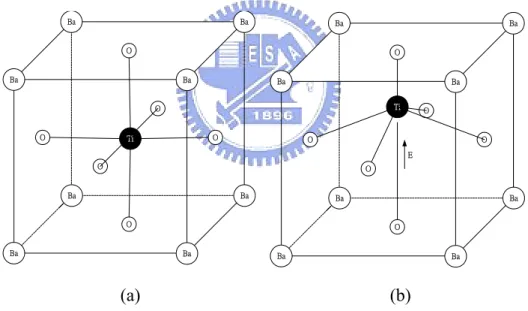
Fig. 1.4 The symmetric perovskite crystal structure (a) is not polarized when there is no applied electric field. And the applied field polarizes the structure (b). (pp. 12)
Fig. 1.5 XRD pattern of Ta thin film oxided at 700 ゚ C for 1, 1.5, 2, 3 and 4 min. (pp. 13)
Fig. 1.6 The evolution of surface morphology resulted from thermal oxidation at 700 ゚ C for 1(a), 3(b) and 4(c) min. (pp. 14)
Fig.f1.7aaaSchematic of the relevant energy levels for XPS binding energy measurements. Note that a conduction specimen and spectrometer are in electrical contact ant thus have common Fermi levels. (pp. 15)
Fig. 1.8 Illustration of band gap energy by O 1s or N 1s photoelectron energy loss spectrum. (pp. 15)
Chapter 2
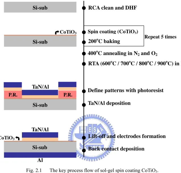
Fig. 2.1 The key process flow of sol-gel spin coating CoTiO3. (pp. 19)
Chapter 3
Fig.a3.1 TEM image of Al-electrode/1-coated CoTiO3 thin film/bare Si structure.
(pp. 24)
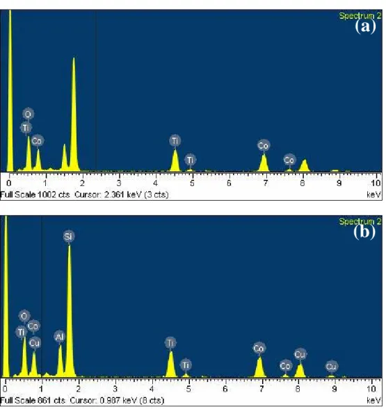
Fig.a3.2aaaElectron dispersive spectra (EDS), associated with the TEM image showed in Fig. 3.1, of the CoTiO3 dielectric annealed at 400 ゚ C. (pp. 24)
Fig.a3.3 XRD Spectra of spin-on CoTiO3 films. The marked peaks correspond to
crystallized CoTiO3 phases. (pp. 25)
Fig. 3.4 SPM images of spin-on CoTiO3 films with various thermal treatments at (a)
200oC, (b) 400oC, (c) 600oC, (d) 700oC, (e) 800oC and (f) 900oC. The image size is 1 μm by 1 μm. (pp. 31)
Fig. 3.5 Surface roughness of spin-on dielectrics as functions of annealing temperature. (pp. 32)
Fig. 3.6 Auger depth profile of the CoTiO3 dielectric annealed at 600oC. (pp. 32)
Fig. 3.7 ESCA spectra of Si 2p(a), O 1s(b), Co 2p(c) and Ti 2p(d) with different annealing temperature. (pp. 33)
Fig. 3.8 ESCA spectra of Co 2p(a), Ti 2p(b) and O 1s(c) for the spin-on dielectric annealed at 600oC. (pp. 34)
Chapter 4
Fig. 4.1 TEM micrograph of an ultrathin CoTiO3 film spin-coated on a high quality
thermal SiO2 layer and annealed at 600oC. (pp. 38)
Fig. 4.2 C-V curves of capacitors with TaN/CoTiO3/SiO2/Si and TaN/SiO2/Si stack
Fig. 4.3 C-V curves of spin-on CoTiO3 films with different thermal treatments.
(pp. 39)
Fig. 4.4 I-V curves of spin-on CoTiO3 films with different thermal treatments.
(pp. 39)
Fig. 4.5 Effective oxide thickness and current density of spin-on dielectrics as functions of annealing temperature. (pp. 40)
Fig. 4.6 I-V curves measured at RT and elevated temperatures. (Inset) Extracted Schottky-emission barrier heights. (pp. 41)
Fig. 4.7 Effective barrier heights extracted from I-V curves by using Schottky-emission and Frenkel-Poole models. (pp. 41)
Fig. 4.8 ESCA spectra of O 1s for thermally grown 15 nm-SiO2. (pp. 42)
Fig. 4.9 ESCA spectra of O 1s for the spin-on 15 nm-CoTiO3 dielectric annealed at
600oC. (pp. 42)
Fig. 4.10 Maximum valence energy band spectra of thermally grown 15 nm-SiO2
and spin-on 20 nm CoTiO3 dielectric annealed at 600oC measured by
high resolution ESCA. (pp. 43)
Fig. 4.11 Band alignment between Si, SiO2 and spin-on CoTiO3 dielectric with
Chapter 1
Introduction
In this chapter, the reasons for why traditional silicon dioxide should be replaced by high-κ gate dielectrics will be addressed. Then the fundamental properties of high-κ materials will be introduced. We will briefly illustrate the requirements for high-κ gate dielectrics. Finally, we will introduce the method of sol-gel spin coating used in this thesis and the ESCA analyzing technique.
1.1 Motivation of High-
κ
Gate Dielectrics Project
The speedy progress of complementary metal-oxide-semiconductor(CMOS) integrated circuit technology has made our chips more powerful, even cheaper and met several requirements. The requirements include higher speed, lower consumption, and so on. And these have been accomplished by scaling down the transistor feature size, such as channel length and gate silicon-oxide (SiO2) thickness. According to
Moore’s law, an exponential growth in the number of transistors per chip was predicted and had been proven true as shown in figure 1.1 [1].
One reason that Si-based devices have played the main roles in microelectronic fabrication is that Si has a high quality and easily-formed SiO2. And it exhibits low
trap density, large band gap, low interface state density, high carrier mobility and good thermal stability with Si. Unfortunately, significant gate leakage current increases and boron penetration occurs when SiO2 is scaled less than 30Å as shown in
figure 1.2 [2]. However, a temporary solution, silicon nitride or oxynitride(SiOxNy),
relaxes the problems. SiOxNy owns slightly higher dielectrics constant(κ~7.5)and
which reduces the gate leakage current due to thicker physical film. The particular Si-O-N network bonding in SiOxNy greatly suppresses boron penetration through the
not high enough. And it is necessary to find a candidate material which has higher dielectric constant for replacing conditional gate dielectrics.
1.2 Metal Oxide Material for High-
κ
Gate Dielectrics
As the description in the classical electrostatics, the internal polarization P of a substance is induced when an external electric field E is applied on it. And which can be formulated simply as below equation,
(1-1)
where D is the electric displacement and εo is the permittivity of free space. However,
we can rewrite Eq. (1-1) and replace the internal polarization P by a coefficient κ called dielectric constant,
(1-2)
Comparing Eq. (1-1) with Eq. (1-2), therefore, we know that dielectric constant κ is used to tell the degree of the polarization of certain material while the external electrical field is applied.
Figure 1.3 illustrates the relation between the real (εr’) and imaginary (εr”) parts
of the dielectric permittivity and the frequency, and also marks the current frequency range for CMOS operation (100MHz~10GHz) [3]. There are two main contributions to the dielectric constant which give rise to the polarization: electronic and ionic dipoles. In general, atoms with higher atomic number demonstrate more electron dipole response to an external electrical field, because there are more electrons to respond to the field. And this electronic contribution tends to increase the permittivity
D=εoE+P,
at ultrahigh frequency (~1016 Hz) as a result of the light electrons.
The ionic contribution to the permittivity could be much larger than the electronic portion such as (Ba, Sr)TiO3 which exhibits ferroelectric behavior
(perovskite crystal structure) below Curie Temperature. As shown in figure 1.4, Ti ions in the unit cells are displaced in response to an applied electric field. This displacement of Ti ions results in a huge polarization in the material, and thus can give rise to large dielectric constants (SrTiO3 ~175 [4]). Since ions respond more
slowly than electrons to an applied field, the ionic contribution begins to decrease at very high frequency (~1012 Hz), as shown in Figure 1.3.
Furthermore, we can modify the polarization behavior of an insulator by low level incorporation. This low level incorporation actually changes the localized bonding order and the vibration mode of the network ions in that insulator. G.. Lucovsky and B. Rayner demonstrated this phenomenon by low level doping Zr (or Hf) atoms in the SiO2 film; and the dielectric constant of the insulator increased due
to the discernable change in bonding order and in vibration modes [5].
In summary, we can briefly tell the main contributions to the polarization of insulators for gate dielectrics: electronic, ionic and low level incorporation. However, the above contributions will be distinguished when the atoms own more electrons and higher atomic number. And that’s why metal oxide exhibits higher permittivity than the SiO2.
1.3 Requirements for High-
κ
Gate Dielectrics
In order to successfully replace gate SiO2, the alternative high-κ material should
possesses some required properties for next generation devices. In this section, we are going to talk about this issue.
1.3.1 Permittivity and Barrier Height
As previous discussion, an insulator with higher permittivity reduces the gate leakage current due to thicker physical thickness. However, leakage mechanism actually is dominated by intrinsic properties and is affected by extrinsic properties. The intrinsic properties of the insulator include band gap (Eg), the dielectric constant
(κ) and the conduction band offset (ΔEC). The extrinsic properties of the insulator
include physical thickness, film morphology, the method of deposition, temperature and applied electrical field to the insulator. And several basic conduction processes in insulators are listed in table 1.1 [6].
Therefore, as described in table 1.1, the direct tunneling current will be obviously suppressed by increasing the physical thickness and the conduction band offset.
1.3.2 Thermodynamic Stability on Silicon
So far, most of the studied high-κ metal oxide systems have unstable interfaces with Si; they react with Si to form an undesirable interfacial layer. However, that will reduce the effective oxide thickness (E.O.T.) and degrade the carrier mobility under the interfacial layer [7]. So it is important to understand the thermodynamics of these systems and thereby attempt to control the interface with Si.
Because Si devices will undergo several high temperature processes after high-κ deposition on Si-sub, possible interfacial reaction are given as follows:
(1-3)
(M: metal, MOx: high-κ metal oxide, MSi x: metal silicide, MSiOx: metal silicate)
Si + MOx Æ M + SiO2
Si + MOx Æ MSix + SiO2
Si + MOx Æ MSix + MSiOx
Si + stable MOx + O2 Æ stable MOx + SiO2
(1-3) (1-4) (1-5) (1-6)
Although the interfacial metal-silicon products are usually detrimental to the gate oxide performance, the metal silicate which is shown in Eq. (1-5) is even helpful in some aspects. Taking HfO2 and HfSiO4 for example, the interface and crystallization
temperature of HfSiO4 are sharper and higher than those of HfO2, respectively [7][8].
And we will discuss high-κ material crystallization temperature more detail later. In addition to the issue of thermodynamics stability between high-κ material and bare Si-sub, the Eq. (1-6) describes that the excess oxygen atoms diffuse through the high-κ metal oxide and react with Si at high temperature. Especially in the ultra-thin film regime, this reaction will cause undesirable interfacial layer more easily.
Therefore, in order to precisely control the EOT of high-κ gate oxide and obtain better interface between gate oxide and Si-sub, we need to find certain high-κ metal oxide which has good thermodynamics stability with Si-sub at high temperature.
1.3.3 Interface Quality
A definite goal of any potential high-κ gate dielectric is to have a sufficiently high-quality interface with Si channel, as close as possible to that of SiO2. And the
SiO2 gate dielectric has a midgap interface state density Dit ~2×10¹⁰ states/cm2 [6].
However, most of the investigated high-κ materials represent Dit ~1011-1012states/cm2,
and exhibit a flatband voltage shift ΔVFB > 300mV [7]. Therefore, in order to obtain
an optimal high-κ-Si interface quality, it is critical to understand the origin of the interface properties of any high-κ gate dielectric.
Because of the lattice structure mismatch, there certainly exists some interface defect states between high-κ gate oxide and Si-sub. It is empirically shown that if the average number of bonds per atom Nav>3 at the interface, the interface defect density
will increase proportionally, and the device performance will be degraded also. Metal oxides which contain elements with a high coordination, such as Ta and Ti, will have a high Nav, and form an overconstrained interface with Si. And degradation in leakage
current and electron channel mobility is also observed [9]. Furthermore, the silicide bonding which forms near the Si channel interface will tend to give rise to detrimental bonding conditions, leading to significant leakage current and poor carrier channel mobility.
As mentioned earlier in Eq. (1-6), oxygen atoms may diffuse through the high-κ dielectric and react with Si. And ZrO2 and HfO2 have been studied as having high
oxygen diffusivities [10]. Although we know that there exists better interface between SiO2 and Si-sub ( Dit ~2×10¹⁰ states/cm2), an uncontrolled interfacial SiO2 will
severely compromise the capacitance gain from any high-κ material in that gate stack structure. Therefore, the character of resisting to oxygen diffusion in the annealing ambient should be considered when we are assessing the interface stability of high-κ dielectric.
Furthermore, the ideal gate dielectric stack may well turn out to have an interfacial layer composed of several monolayers of Si-O and a high-κ dielectric is used on the top of the interfacial layer. And this stack structure could possess better quality interface like that of SiO2 and higher capacitance because of the high-κ
material.
1.3.4 Film Morphology
The work by R. Chandrasekharan et al. investigated the film morphology of high-κ dielectric Ta2O5 and recognized the relation between oxidation time and
crystallization temperature [11]. Figure 1.5 shows that no peak of crystalline Ta2O5 is
observed until after 1.5min of oxidation. Between 1.5 and 2 min of oxidation, crystalline phases of Ta2O5 begin to appear. Furthermore, as the oxidation time
increases, the intensity of crystal formation also increases. And figure 1.6 shows that the surface morphology of Ta2O5 film with different oxidation time. For the
3-min-oxided sample, the surface becomes rough and small cracks start to appear while the oxide grains are formed; and the 4-min-oxided one, the surface becomes rougher and more cracks are observed while larger grains are formed.
Because grain boundaries serve as highly leaky paths, it is expected to find a material which remains in an amorphous phase even if the film undergoes high temperature processes.
1.3.5 Gate Compatibility
As mentioned in 1.3.2, when high-κ materials directly contact with Si-sub, they will react with Si and form unfavorable interfacial layers. The similar reactions will also occur when high-κ materials meet poly-Si gate electrodes [12]. Furthermore, the dopant diffusion through high-κ gate dielectric will cause an unfavorable Vth shift
[13][14]. And metal gate is one of possible solutions to suppressing dopant diffusion, poly depletion and sheet resistance constraint. In addition, the use of metal gates in gate processes can lower the thermal budge by eliminating the need for the dopant activation of poly-Si electrode [7].
Since doped poly-Si is the incumbent gate electrode material, it should be carried out to investigate how dopants in poly-Si diffuse through high-κ materials. However, current roadmap predicts that the metal gate technology will replace the doped poly-Si gates [15]. It is therefore necessary to focus efforts on dielectric materials systems which are compatible with potential metal gate materials.
1.3.6 Process Compatibility
There are several studying methods to deposit a high-κ dielectric: physical vapor deposition (PVD) [16], chemical vapor deposition (CVD) [12], molecular beam epitoxy (MBE) [4] and sol-gel spin coating method [17][18][19].
PVD principally includes evaporation and sputtering. Though these two PVD methods could be carried out at normal temperature for unlimited substrate materials,
the poor step coverage is the most challenge to deposit an uniform gate dielectric. In a sputtering process, however, the inevitable plasma damage results in surface damage and thereby creates unwanted interfacial states [7].
CVD mainly involves metal organic chemical vapor deposition (MOCVD) and atomic layer deposition (ALD). Though most of CVD methods have proven to give more uniform step coverage, the ALD method seems to provide much promise to deposit better-quality high-κ gate dielectrics than that of MOCVD. Furthermore, as far as the throughput and the requirements for instrument are concerned, it is obviously that ALD method is better than MOCVD and MBE methods [7].
This study mainly uses the sol-gel spin coating method to form the high-κ gate dielectrics. However, the more detail introduction about this method will be provided in the next section.
1.4 Sol-Gel Spin Coating Method
Recently, many technologies have been used to prepare various high-κ dielectrics, such as atomic layer deposition (ALD), chemical vapor deposition (CVD) and physical vapor deposition (PVD). Nevertheless, the sol-gel spin coating method also catches much attention; it is utilized to form the high-κ dielectric films [17] and memory charge trapping layers [18][19].
In the sol-gel processes, hydrolysis, condensation, and polymerization, the step-by-step formation leads to a metal-oxide network. And there is an arresting character of sol-gel spin coating method and which is an ability to synthesize new types of high-κ materials, called “inorganic-organic hybrid” [20].
The sol-gel spin coating method could be executed in the normal pressure environment rather than high vacuum system. And thin film formation with spin coating is simpler than ALD, PVD, or MBE to deposit an insulator because of its
cheaper precursors and tools.
1.5 Electron Spectroscopy for Chemical Analysis (ESCA)
In this section it is worth introducing the fundamental principle of ESCA because the most following analysis for material and physical properties are performed by ESCA technique.
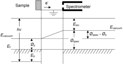
ESCA, also known as XPS, is used to characterize the chemical bonding and film composition. Since the photon energy range of interest for material analysis corresponds to the x-ray energy (1-10 keV), photoelectron spectra with specific binding energies produced by x-ray radiation of a sample present chemical bonding information about given elements. Figure 1.7 shows relevant energy levels for ESCA measurements [21]. Binding energies of photoelectrons can be obtained from Eq. (1-7), based on Figure 1.7.
Ekin =hν −Eb−φspec, (1-7) where Ekin is kinetic energy of the photoelectron, h is Plank’s constant, ν is the
frequency of he photon, Eb is the binding energy, and Øspec is the work-function of the
spectrometer.
However the ejected photoelectrons from ESCA analysis undergo inelastic energy losses due to collective oscillations (plasmon) and single particle excitation (electron-hole band to band transitions). More importantly, the excitation of a single electron from the valence band to the conduction band can also be detected at the onset of plasma energy loss, as illustrated in Figure 1.8 [22]. This onset point of plasma energy loss can be utilized to determine the band gap energy [23-25]. Photo-excited electrons lose their kinetic energies due to collective oscillations of outer shells, resulting in a plasmon spectrum. Single electron excitation from valence
band edge to conduction band edge also takes place at the onset of a plasmon spectrum. Ec, Ev, Eg, and hν denote conduction band minimum, valence band
Figure 1.2 Calculated(lines)and measured(dots)results for tunneling currents from inversion layers through oxides [2]. Figure 1.1 Moore’s law for microelectronic industry. The exponential increase of transistors count as a function of time for distinct generations of microelectronics has been realized [1].
Ba Ba Ba Ba Ba Ba Ba Ba O O O O O O Ti Ba Ba Ba Ba Ba Ba Ba Ba O O E O O O O Ti
Fig. 1.4 The symmetric perovskite crystal structure (a) is not polarized when there is no applied electric field. And the applied field polarizes the structure (b).
Figure 1.3 The frequency dependence of the real (εr’) and
imaginary (εr”) parts of the dielectric permittivity. In CMOS
devices, ionic and electronic contributions are present.
Fig. 1.5 XRD pattern of Ta thin film oxided at 700 ゚ C for 1, 1.5, 2,3 and 4 min [11].
Fig. 1.6 The evolution of surface morphology resulted from thermal oxidation at 700 ゚ C for 1(a), 3(b) and 4(c) min [11].
Fig. 1.8 Illustration of band gap energy by O 1s or N 1s photoelectron energy loss spectrum.
Fig. 1.7 Schematic of the relevant energy levels for XPS binding energy measurements. Note that a conducting specimen and spectrometer are in electrical contact and thus have common Fermi levels.
Schottky Emission Frenkel-Poole Emission Direct Tunneling Fowler-Nordheim Tunneling Hopping (Ohmic) Conduction
Table 1.1 Basic conduction processes in insulators [6]. ⎟⎟ ⎠ ⎞ ⎜⎜ ⎝ ⎛ − + kT q T V a T J ~ 2exp φB ⎟⎟ ⎠ ⎞ ⎜⎜ ⎝ ⎛ − + kT q T V a V J ~ exp 2 φB ⎥ ⎥ ⎦ ⎤ ⎢ ⎢ ⎣ ⎡ ⎟ ⎠ ⎞ ⎜ ⎝ ⎛Φ − − 2 2 2 exp 1 ~ 2 * 2 diel B diel diel V q m t t J h ⎟ ⎠ ⎞ ⎜ ⎝ ⎛− V b V J ~ 2exp ⎟ ⎠ ⎞ ⎜ ⎝ ⎛ ′ − T c V J ~ exp
Chapter 2
Experimental Procedures
In this chapter we will illustrate the device fabrication process with figures and list the instruments for material and physical properties measurements.
2.1 Device Fabrication
In this investigation, CoTiO3 films were prepared by sol-gel spin coating method
in a controlled environment, where was maintained at 22oC and 43 % RH. The
process flow was illustrated in figure 1. First, n-type single crystal Si wafers with resistivity 4-7 Ωcm underwent standard RCA cleaning followed by a dilute-HF dip to remove the native SiO2. Then, the sol-like precursor for CoTiO3 was directly spun on
the Si substrates at about 3000 revolutions per minute, and the spin speed was maintained for 30 seconds. However the precursor for cobalt and titanium elements were cobalt acetate tetrahydrate Co(OOCCH3)2.4H2O and titanium isopropoxide
Ti(OCHC2H6)4, respectively. These two precursors were dissolved in
2-methoxyethanol for spin coating method. After the spin-coating of the precursor, in order to remove the solvent, the samples were baked at 90oC for 1.5 min on a hotplate.
And the procedure (coating-and-baking) was repeated for 5 times. Afterward the films were oxidized at 400oC in an N2/O2 ambient for 10 min, in which both N2 and O2 flow
were 50 sccm. In order to study the properties of CoTiO3 high-k dielectrics after high
temperature treatment, rapid thermal annealing (RTA) was performed. The samples were annealed at 600oC, 700oC, 800oC or 900oC for 30s in N
2 ambient.
Photolithography was used to define gate areas and then TaN metal was deposited on the top of samples by reactive DC-sputtering. Lift-off was performed to form the MIS capacitors. Thereafter, ohmic contacts were formed by thermal evaporation of 300-nm-thick aluminum (Al) electrode on the backside of the samples.
2.2 Material and Physical Properties Measurements
The microstructure of spin-on CoTiO3 film and Si substrate were studied by
JEOL JEM-2100F field emission transmission electron microscopy (TEM) equipped with Link ISIS-300 energy dispersive X-ray analyzer (EDS). And the TEM EDS with a 5-nm electron beam probe was used to perform chemical analysis qualitatively.
The characteristic of crystallization of spin-on CoTiO3 films with different
annealing temperature were identified by PANalytical X’Pert Pro X-ray diffraction system under normal atmosphere. Optical module with X-ray mirrors and a parallel plate collimator was used to perform gracing incident X-ray diffraction (angle of incidence θi ~1˚). The beam source originated from Cu Kα radiation with a 0.154-nm
wavelength and this beam source was operating at 1.8 kW.
Surface morphology of spin-on CoTiO3 films with different annealing
temperature was obtained by Veeco dimension 5000 scanning probe microscope (SPM) under normal atmosphere. The highest resolution in X-Y plane and Z direction were about 1.5 nm and few angstroms, respectively. And the tip curvature radius was about 2 nm.
A ULVAC-PHI Quantera high resolution X-ray photoelectron spectrometer (HR-XPS) with 180˚ spherical capacitor analyzer was used to analyze quantitatively the chemical composition of the dielectrics CoTiO3 prepared by sol-gel coating
method.
The capacitance-voltage (C-V) curves and current-voltage (I-V) curves were measured in the same probe station by HP 4284 and Keithly 4200, respectively.
● ● ● ● ● ● ● ●
● RCA clean and DHF
Spin coating (CoTiO3)
200oC baking Repeat 5 times
400oC annealing in N2 and O2
RTA (600oC / 700oC / 800oC / 900oC) in N2
Define patterns with photoresist
Lift-off and electrodes formation TaN/Al deposition
Back contact deposition
Fig. 2.1 The key process flow of sol-gel spin coating CoTiO3.
CoTiO3 P.R. P.R. TaN/Al CoTiO3 TaN/Al Si-sub Si-sub Si-sub Si-sub Al
Chapter 3
Material Properties
In this chapter, we will report the material properties of spin-on CoTiO3 thin
films analyzed by Transmission Electron Microscope (TEM), Energy Dispersive Spectrometer (EDS), Grazing Incident X-Ray Diffraction (GI-XRD), Scanning Probe Microscope (AFM), Auger Electron Microprobe (AEM) and Electron Spectroscopy for Chemical Analysis (ESCA).
3.1 Si-sub/CoTiO
3Interface Quality
In figure 3.1, the graph is the cross-section of Al-electrode/1-coated CoTiO3 thin
film/bare Si substrate structure and the CoTiO3 thin film is annealed at 400oC. There
are two interfacial layers astride the CoTiO3 thin film. The interfacial layer between
Si-sub and CoTiO3 thin film is about 2.23 nm and the interfacial layer between
Al-electrode and CoTiO3 thin film is about 1.88 nm. Furthermore, the thickness of the
1-coated CoTiO3 thin film on Si-sub is about 5.27 nm.
In order to qualitatively recognize the composition of the spin-on dielectric, EDS analysis is performed. As shown in figure 3.2 (a), the three principal elements, Cobalt, Titanium and oxygen, are detected. However, as shown in figure 3.2 (b), Al peak and Si peak maybe come from the interfaces beside the dielectric, and the Cu peak should be contributed to the Cu net which is used to hold the sample. Therefore there are three main elements, cobalt, titanium and oxygen in the spin-on dielectric.
3.2 Surface Morphology
As mentioned in section 1.3.4, it is desirable that the surface morphology of high-κ dielectric is still smooth though it undergoes high temperature treatment. PANalytical X'Pert Pro (XRD) and Veeco Dimension 5000 Scanning
Probe Microscope (D5000) are used to analysis surface morphology of films with different high temperature annealing.
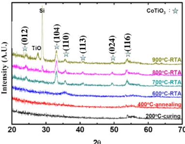
Figure 3.3 presents the GI-XRD spectra of the CoTiO3 thin films. No significant
signals could be found for samples treated at temperatures below 600oC, indicating amorphous CoTiO3 films to begin with. When a sample was annealed at a temperature
above 700oC, signals of crystallized CoTiO3 phases were found. This suggests the
crystallization temperature of spin-on CoTiO3 films being 600~700°C. Furthermore,
signals of Si substrates were also found in the GI-XRD spectra for samples annealed at temperatures beyond 800oC. It is speculated that the crack of CoTiO3 films has
partially exposed the Si substrate after annealed at elevated temperatures.
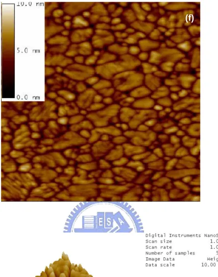
Figure 3.4 shows the SPM images of CoTiO3 films with different high
temperature treatments. From figure 3.4(a) to figure 3.4(f) are the flattened and 3-D images of samples baked or annealed at 200oC, 400oC, 600oC, 700oC, 800oC, and 900oC, respectively. The extended dark regions was found in the images for 600~900oC annealed samples. Serious cracks of the CoTiO3 thin film can be found
after annealed at 900oC, as shown in figure 3.4(f). And figure 3.5 reports that the roughness of samples suddenly becomes serious when annealing temperature is higher than 600 oC.
3.3 Composition Analysis
3.3.1 Auger Electron Microscope Analysis
The incorporation of carbon element in a dielectric will decrease the effective dielectric constant [26]. Therefore Auger depth profile is used to analyze the elements in spin-on dielectric CoTiO3 with 600oC annealing. As shown in figure 3.6, it is
obvious that carbon element signal only exists at the start of analysis, i.e. at surface. The surface carbon may be resulting form the absorption of residual in the air. Hence
there is no carbon element in the dielectric formed by this sol-gel spin coating method.
In this analysis, because we didn’t have the reference sample to derive the relative sensitivity factor for evaluating atomic concentration in depth profile, there is an error in the atomic percentage in the figure 3.6. Despite this deviation, the qualitative composition result could be acceptable.
3.3.2 Electron Spectroscopy for Chemical Analysis
There is no doubt that the spin-on dielectrics only contains cobalt, titanium and oxygen elements, which is confirmed by EDS analysis in section 3.1 and Auger depth profile in section 3.1. However, we still don’t know the chemical properties and atomic concentration ratio of this dielectric prepared by sol-gel spin coating. In the section we use electron spectroscopy for chemical analysis (ESCA) to obtain further information.
Figure 3.7 shows ESCA results of the dielectric formed by sol-gel spin coating method and the dielectric under analysis is 1-coated and annealed at 600oC. From figure 3.7(a) to 3.7(d) are the spectrums of silicon 2p orbital, oxygen 1s orbital, cobalt 2p orbital and titanium 2p orbital, respectively. As shown in figure 3.7(a), two main peaks identify single crystalline silicon (99.3 eV) and silicon dioxide (103.3 eV) in the silicon 2p orbital spectrum. We also observe that the shift and the growth of the silicon-dioxide-peak increases, as the annealing temperature is increased, which means that more complete structure and thicker silicon oxide are formed after higher temperature annealing. The spectrum of oxygen 1s orbital shown in figure 3.7(b) reveals that there may be two kinds of metal-oxygen bonds with lower binding energy near 531 eV , e.g. Co-O and Ti-O for all samples. However, the broader binding energy distribution for the sample annealed at 200oC may be resulting from hydroxides in the dielectric [27]. Furthermore, the samples with 800oC and 900oC
annealing have silicon oxide bond with binding energy near 533 eV, which is consistent with the results in figure 3.7(a). We also notice that two shake-up peaks with higher binding energy than two main peaks (2p3/2 and 2p1/2) appear in the Co
spectrum, as shown in figure 3.7(c).
In order to confirm the atomic concentration ratio of the dielectric prepared by sol-gel spin coating method, more detailed ESCA analysis for the spin-on dielectric annealed at 600 oC is executed. After background removal by Shirley method and curve fitting for oxygen-metal bonds (oblique line area) in oxygen spectra, we integrate the intensity from 775 to 810 eV for cobalt spectra, from 453 to 468 eV for titanium spectra and from 527 to 535 eV for oxygen spectra, as shown in figure 3.8. The relative sensitivity factors for cobalt, titanium and oxygen are 3.529, 2.077 and 0.733, respectively. And the atomic concentration ratio is obtained as,
93175.67 53580.63 53828.65 [ ]:[ ]:[ ] : : : : 3.529 2.077 0.733 Co Ti O Co Ti O A A A Co Ti O SF SF SF = = 1: 0.97 :3.04 ≈ .
5nm
Fig. 3.1 TEM image of Al-electrode/1-coated CoTiO3
thin film/bare Si structure.
Fig. 3.2 Electron dispersive spectra (EDS), associated with the TEM image showed in Fig. 3.1, of the CoTiO3dielectric annealed at 400oC.
1.88 nm
5.27 nm
2.23 nm
(a)
(b)
Al
CoTiO
3Si-sub
Fig. 3.3 XRD spectra of spin-on CoTiO3 films. The marked
peaks correspond to crystallized CoTiO3 phases.
(012) (104) (1 10) (1 13) (024) (1 16)
(f)
Fig. 3.4 SPM images of spin-on CoTiO3 films with various thermal treatments
at (a) 200oC, (b) 400oC, (c) 600oC, (d) 700oC, (e) 800oC and (f) 900oC. The image size is 1 μm by 1 μm.
200
400
600
800
1000
0
3
6
9
12
R.
M
.S.
(A
)
temperature (C)
0
20
40
60
80
100 120
0
20
40
60
80
100
A
tom
ic Concent
rat
io
n (
%
)
Sputtering Time (sec)
C
Ti
O
Co
Si
Fig. 3.5 Surface roughness of spin-on dielectrics as functions of annealing temperature.
543 540 537 534 531 528 525 (b) Metal Oxides SiO2 RTA900 RTA800 RTA700 RTA600 furnace curing O 1s In te n s ity (a .u .)
Binding Energy (eV)
810 800 790 780 770 (c) curing RTA900 RTA800 RTA700 RTA600 furnace 2p1/2 2p3/2 Co Int ens ity ( a. u. )
Binding Energy (eV)
470 465 460 455 450 (d) RTA600 RTA800 RTA700 RTA600 curing furnace 2p1/2 2p3/2 Ti In ten s it y (a.u .)
Binding Energy (eV)
110 108 106 104 102 100 98 96 (a) SiO2 Si RTA900 RTA800 RTA700 RTA600 furnace curing Si 2p In te n s it y (a .u .)
Binding Energy (eV)
Fig. 3.7 ESCA spectra of Si 2p(a), O 1s(b), Co 2p(c) and Ti 2p(d) with different annealing temperature.
810 800 790 780 0 2 4 6 8 10 12 (a) 2p1/2 2p3/2 Co unt s ( x 1 0 3 /s )
Binding Energy (eV) Co 468 465 462 459 456 453 0 3 6 9 12 15 18 21 (b) 2p3/2 2p1/2 C o u n ts (x 10 3 /s )
Binding Energy (eV) Ti 534 532 530 528 -5 0 5 10 15 20 25 30 35 (c) metal oxide SiO 2 C ount s ( x10 3 /s )
Binding Energy (eV) O 1s
Measured Fitted
Fig. 3.8 ESCA spectra of Co 2p(a), Ti 2p(b) and O 1s(c) for the spin-on dielectric annealed at 600oC.
Chapter 4
Physical Property
In this chapter, we will report the physical properties of spin-on CoTiO3 thin
films, such as dielectric permittivity, C-V and I-V characteristics, current transport mechanism, band energy gap and band alignment.
4.1 Dielectric Permittivity
According to section 3.1.1, it is easy to form an interfacial layer between Si-sub and a CoTiO3 film. However, it is imprecise and difficult to extract the κ value of
CoTiO3 film from measuring capacitance. In order to estimate the dielectric constant
of CoTiO3 thin films, a thermal oxidation is used to grow a high quality SiO2 thin
layer before the CoTiO3 spin-coating. The C-V characteristics of both
TaN/CoTiO3/SiO2/Si and TaN/SiO2/Si capacitors are demonstrated in Fig. 4.1. The
well C-V characteristics can be observed for both two capacitors without flat-band voltage shift, as shown in Fig. 4.1. The capacitance effective thickness (CET) is extracted from C-V curves at 100 kHz without considering quantum effect. The CET of CoTiO3/SiO2 and SiO2 are 4.66nm and 4.27nm, respectively. However figure 4.2
shows HR-TEM image of the Si/SiO2/CoTiO3/TaN structure. Thicknesses of 1-coated
high-k dielectric and thermal oxide are 4.02 and 4.27 nm, respectively, as shown in this TEM image. As a result, the exact dielectric constant of CoTiO3 thin film is found
to be 40.2, which is matched the value of CoTiO3 films fabricated by direct oxidation
of sputtered Co/Ti layers [28][29], indicating that the high permittivity CoTiO3 films
can also been deposited by simple sol-gel spin coating method.
4.2 C-V and I-V Characteristics
thermal treatments. The sample with 600oC RTA shows a steeper C-V slope in the depletion region, suggesting a better CoTiO3/Si interface. RTA temperatures beyond
600oC result into flatter C-V curves which may be due to the sub-stoichiometric interfacial-oxide growth and thermal stress.
Figure 4.4 shows the I-V characteristics of CoTiO3 gate dielectrics. The leakage
current density increases with increasing RTA temperature (600~900oC), even though the C-V curves suggest a larger effective oxide thickness (EOT) for samples annealed at higher temperatures. This can be explained by the cracks and crystallization of CoTiO3 thin films, as discussed before. Finally we sum up the fundamental electrical
behavior of spin-on CoTiO3 dielectric in figure 4.5, and the dielectric annealed at
600oC has the smallest EOT.
4.3 Current Transport Mechanism
Figure 4.6 shows the I-V curves measured at elevated temperatures. The CoTiO3
film under test was annealed at 600oC. The I-V curves were fitted by the Schottky emission model (inset), and the barrier heights of 0.74, 0.72, 0.70, and 0.69eV were extracted at room temperature, 40oC, 50oC, and 60oC, respectively. Fittings with the Frenkel-Poole (FP) conduction model were also carried out. Figure 4.7 demonstrates that the current conduction is not dominated by the FP conduction but by the Schottky emission, which shows a smaller Si/CoTiO3 barrier height.
4.4 Band Energy gap and Band Alignment
As mentioned in Section 1.5, XPS technique can be utilized to determine the band gap energy. In this section we characterize the band gaps of SiO2 and the spin-on
CoTiO3 dielectric annealed at 600oC. In order to align the band diagram, we also use
thermally grown SiO2 and the spin-on CoTiO3 dielectric [30].
As mentioned in Section 1.5, the background rise below XPS core level peaks is due to inelastic scattering effects of the photon-electrons. More importantly, the excitation of the electrons from valence band to conduction band can also be detected at the onset of plasma energy loss. As a result, the onset of the background increase relative to the peak position corresponds with the band gap of the material. Figure 4.8 shows the spectrum of oxygen 1s orbital for SiO2, which is illustrating that the energy
band gap of thermal SiO2 is about 9.0 eV. This value is almost close to the common
results [6][7]. Furthermore, the high resolution core level and band gap spectra of spin-on CoTiO3 film is shown in Fig. 4.9. The energy band gap of spin-on CoTiO3 is
about 2.2 eV, which is close to the value of CoTiO3 powders fabricated by a modified
Pechini method [31].
On the other hand, the measurements are performed on thermal SiO2 (~15nm)
and the 5-coated dielectric CoTiO3 (~20nm)/SiO2 (~15nm) stacks. The valance band
spectrum for these layers contains the information about the density of states of both the CoTiO3 and SiO2 films. The maximum valence energy band and the valence band
offset (ΔEv) between CoTiO3 and SiO2 films can thus be determined as about 4.0 eV,
as indicated in Fig. 4.10.
As mention in figure 4.7, the energy barrier height between silicon substrate and spin-on CoTiO3 dielectric is about 0.74 eV at room temperature. Because the energy
band alignment between Si and SiO2 is a well-known result, we can deduce the band
alignment between Si, SiO2 and spin-on CoTiO3 dielectric, as shown in figure 4.11.
Figure 4.11 shows the energy band alignment between Si, SiO2 and high-k dielectric
CoTiO3, which serves to summarize the key results we have obtained from the
analysis of HR-XPS and Schottky emission characteristics. And this deduction is consistent with the result in figure 4.9.
Fig. 4.1 TEM micrograph of an ultrathin CoTiO3 film spin-coated
on a high quality thermal SiO2 layer and annealed at 600oC.
Fig. 4.2 C-V curves of capacitors with TaN/CoTiO3/SiO2/Si
Fig. 4.4 I-V curves of spin-on CoTiO3 films with
different thermal treatments.
Fig. 4.3 C-V curves of spin-on CoTiO3 films
200 400 600 800 1000 10 100 EOT Jg@Vg=2V Temperature (oC) E. O .T. (nm ) 1E-6 1E-5 1E-4 1E-3 0.01 0.1 J (A /c m 2 )
Fig. 4.5 Effective oxide thickness and current density of spin-on dielectrics as functions of annealing temperature.
Fig. 4.7 Effective barrier heights extracted from I-V curves by using Schottky-emission and Frenkel-Poole models.
Fig. 4.6 I-V curves measured at RT and elevated temperatures. (Inset) Extracted Schottky-emission barrier heights.
550 545 540 535 530 525 SiO 2 O 1s 9.0 eV In te n s it y (a .u .)
Binding Energy (eV)
550
545
540
535
530
525
9
12
15
18
21
24
27
C
o
u
n
ts
(x
1
0
4/s
)
Binding Energy (eV)
2.2 eV CoTiO3
O 1s
Fig. 4.8 ESCA spectra of O 1s for thermally grown 15 nm-SiO2.
Fig. 4.9 ESCA spectra of O 1s for the spin-on 15 nm-CoTiO3
14 12 10 8 6 4 2 0 -2 -4 SiO2 CoTiO3 CoTiO3 SiO2 ΔVBmax=4.0 eV In te n s it y ( a .u .)
Binding Energy (eV)
SiO2 Si-sub
CoTiO3
4. 0 eV 4. 4 eV
Eg=2.2 eV Eg=1.1 eV
Ec=0.7 eV
Fig. 4.11 Band alignment between Si, SiO2 and
spin-on CoTiO3 dielectric with 600oC annealing.
Fig. 4.10 Maximum valence energy band spectra of thermally grown 15 nm-SiO2 and spin-on 20 nm CoTiO3 dielectric annealed at
Chapter 5
Conclusions
In this chapter we will summarize the important results of spin-on CoTiO3 as
mentioned in previous chapters and make conclusions for this these.
5.1 Conclusions
In this thesis we form the dielectric CoTiO3 by sol-gel spin coating method
followed by different annealing temperature 600~900oC. The image of transmission electron microscopy (TEM), as shown in Fig. 3.1, reveals that 2.2 nm interfacial layer is between Si-sub and CoTiO3 with 400oC annealing. According to X-ray diffraction
(XRD) pattern in Fig. 3.3, crystallization temperature of the spin-on dielectric is between 600 and 700oC. As shown in Fig. 3.4 and Fig. 3.5, scanning probe microscope (SPM) describes surface morphology of the spin-on dielectrics with different annealing temperature and the surface roughness abruptly increases as annealing temperature higher than 600 oC. Electron spectroscopy for chemical analysis (ESCA) in Fig. 3.7 shows that higher temperature annealing results in thicker interfacial layer and pure chemical bonding. Furthermore ESCA in Fig. 3.8 also confirms that the spin-on dielectric with 600oC annealing has atomic concentration ratio [Co]:[Ti]:[O]~1:1:3. The spin-on film CoTiO3 with 600oC annealing has
Schottky emission conduction mechanism for the TaN/ CoTiO3/ Si-sub structure and
the evidences are presented in Fig. 4.6 and Fig.4.7. And the trapping characteristics of spin-on film CoTiO3 with 600oC annealing is affected by temperature, applied stress
voltage and stress time.
High electrical permittivity (k~40.2) of CoTiO3 dielectric is extracted via the
high resolution transmission electron microscopy (HR-TEM) image and C-V curves, as shown in Fig 4.1 and Fig. 4.2. In addition, the band energy gaps of thermally
grown SiO2 and spin-on CoTiO3 are 9.0 and 2.2 eV, respectively, as shown in Fig. 4.8
and Fig. 4.9. The valence energy band offset between thermally grown SiO2 and
spin-on CoTiO3 is about 4.0eV, which is detected by high resolution X-ray
photoelectron spectroscopy (HR-XPS) in Fig. 4.10. The energy band alignment of spin-on CoTiO3 directly with SiO2 and indirectly with Si is successfully determined in
Reference
[1] B. G. Streetman and S. Banergee, Solid State Electronic Device, 5th ed.: Prentice Hall Inc., 2000.
[2] S.-H. Lo, D. A. Buchanan, Y. Taur, and W. Wang, "Quantum-Mechanical Modeling of Electron Tunneling Current from the Inversion Layer of Ultra-Thin-Oxide nMOSFET's," Electron Device Letters, IEEE, vol. 18, pp. 209-211, 1997.
[3] S. O. Kasap, Principles of Electrical Engineering Materials and Devices: McGraw-Hill, 2002.
[4] K. Eisenbeiser, J. M. Finder, Z. Yu, J. Ramdani, J. A. Curless, J. A. Hallmark, R. Droopad, W. J. Ooms, L. Salem, S. Bradshaw, and C. D. Overgaard, "Field effect transistors with SrTiO3 gate dielectric on Si," Applied Physics Letters,
vol. 76, pp. 1324-1326, 2000.
[5] G. Lucovsky and B. Rayner, "Microscopic Model for Enhanced Dielectric Constants in Low Concentration SiO2-Rich Noncrystalline Zr and Hf Silicate Alloys," Appl. Phys. Lett., vol. 77, pp. 2912, 2000.
[6] S. M. Sze, Physics of Semiconductor Devices, 1985.
[7] G. D. Wilk, R. M. Wallace, and J. M. Anthony, "High-k Gate Dielectrics: Current Status and Materials Properties Considerations," J. Appl. Phys., vol. 89, pp. 5243, 2001.
[8] G. D. Wilk and R. M. Wallace, Appl. Phys. Lett., vol. 74, pp. 2854, 1999. [9] G. Lucovsky, Y. Wu, H. Niimi, V. Misra, and J. C. Phillips, Appl. Phys. Lett.,
vol. 74, pp. 2005, 1999.
[10] A. Kumar, D. Rajdev, and D. L. Douglass, J. Am. Chem. Soc., vol. 55, pp. 439, 1972.
[11] R. Chandrasekharan, Inkyu Park, R. I. Masel, and M. A. Shannon, "Thermal Oxidation of Tantalum Films at Various Oxidation States from 300 to 700 ゚ C," J. Appl. Phys., vol. 98, pp. 114908, 2005.
[12] I. C. Kizilyalli, R. Y. S. Huang, P. K. Roy, "MOS Transistors with Stacked SiO2 –Ta2O5 –SiO2 Gate Dielectrics for Giga-Scale Integration of CMOS
Technologies," Electron Device Letters, IEEE, vol. 19, pp. 423-425, 1998. [13] D. G. Park, H. J. Cho, et al. (2000). Tech. Dig. VLSI Symp.
[14] J. H. Lee, K. Koh, et al. (2000). Tech. Dig. Int. Electron Devices Meet.
[15] The International Technology Roadmap for Semiconductors, Semiconductor Industry Association.
[17] Kuo-Hsing Kao, Jian-Hao Chen, et al. (2007). Characterization of CoTiO3 Thin Films Formed by Sol-Gel Spin Coating with High Temperature Annealing. SNDT, Taiwan.
[18] Hsin-Chiang You, Tze-Hsiang Hsu, et al. (2006). "Hafnium Silicate Nanocrystal Memory Using Sol–Gel-Spin-Coating Method." Electron Device Letters, IEEE 27: 644.
[19] Ko, F.-H., Hsin-Chiang You, et al. (2007). "Fabrication of SONOS-Type Flash Memory with the Binary High-k Dielectrics by the Sol-Gel Spin Coating Method." Jouranl fo The Electrochemial Society 154.
[20] J. Tang, J. Fbbri, et al. (2004). Chem. Mater 16: 1336.
[21] L.C. Feldman and J.W. Mayer, Fundamentals of Surface and Thin Film Analysis, Elsevier Science Publishing Co., Inc., 1986.
[22] D.A. Shirley, Photoemission in Solids І, Vol. 26 of Topics in Applied Physics, edited by M. Cardona and L.Ley (Springer-Verlag, Berlin, 1978), p.165.
[23] S. Miyazaki, H. Nishimura, M.Fukuda, L. Ley, and J. Ristein, Appl. Sur. Sci. 113/114, 585-589 (1997).
[24] J.L. Alay and M. Hirose, J. Appl. Phys., 81, 1606, (1997).
[25] H. Itokawa, T. Maruyama, S. Miyazaki, and M. Hirose, Extended abstracts of the 1999 Int. Conf. Solid State Devices and Materials, Tokyo, 1999, p. 158. [26] Hyeong Joon Kim, Qingyi Shao, Yoon-Hae Kim. Surface and Coatings
Technology, 171 (2003), 39–45.
[27] John F. Moulder, William F. Stickle, Peter E. Sobol, Kenneth D. Bomben, Handbook of X-ray Photoelectron Spectroscopy, Perkin-Elmer Corporation, 1992
[28] T. M. Pan, et al Appl. Phys. Lett. 78, (2001) 1439 [29] J. H. Chen, et al J. Electrochem. Soc., 154, (2007) [30] F.G. Bell and L. Ley, Phys. Rev. B, 37, p.8383, (1988).
[31] Yi-Jing Lin, Yen-Hwei-Chang, et al. (2005). "Synthesis and Characterization of Ilmenite NiTiO3 and CoTiO3 Prepared by a Modified Pechini Method."
Jouranl of Non-Crystalline Solid, 352 789-794. [32] K. Kukli, et al J. Appl. Phys. 92, 5698 (2002).
Publication List
A. International Journal Paper:
[A-1] Ming-Wen Ma, Tien-Sheng Chao, Kuo-Hsing Kao, Jyun-Siang Huang, and Tan-Fu Lei, “Fringing electric field effect on 65-nm-node fully depleted silicon-on-insulator devices,” Japanese Journal of Applied Physics, vol. 45, no. 9A, pp.6854-6859, 2006.
[A-2] Ming-Wen Ma, Chin-Yang Chen, Chun-Jung Su, Woei-Cherng Wu,
Kuo-Hsing Kao, Tien-Sheng Chao, and Tan-Fu Lei, “Reliability mechanisms of LTPS-TFT with HfO2 gate dielectric: PBTI, NBTI and hot carrier stress,”
IEEE Trans. Electron Devices, have been accepted for publication.
[A-3] Ming-Wen Ma, Chin-Yang Chen, Chun-Jung Su, Woei-Cherng Wu, Tsung-Yu Yang, Kuo-Hsing Kao, Tien-Sheng Chao, and Tan-Fu Lei, “Improvement on performance and reliability of TaN/HfO2 LTPS-TFTs with fluorine
implantation,” Solid State Electronics, vol. 52, no. 3, pp.342-247, 2008.
B. International Letter Paper:
[B-1] Kuo-Hsing Kao, Shiow-Huey Chuang, Jian-Hao Chen, Ming-Wen Ma, and Tien-Sheng Chao, “High resolution XPS energy band alignment of CoTiO3
high-k dielectric prepared by sol-gel spin coating method,” Appiled Physics
Lett., in revision.
[B-2] Ming-Wen Ma, Yi-Hong Wu, Kuo-Hsing Kao, Woei-Cherng Wu, Tien-Sheng Chao, and Tan-Fu Lei, “Impacts of N2 and NH3 plasma surface-treatment on
high performance LTPS-TFT with high-κ gate dielectric,” IEEE Electron
Device Lett., in version.
[B-3] Ming-Wen Ma, Tien-Sheng Chao, Kuo-Hsing Kao, Jyun-Siang Huang, and Tan-Fu Lei, “High-κ material sidewall with source/drain-to-gate non-overlapped structure for low standby power applications,” Japanese
Journal of Applied Physics, vol. 45, no. 11, pp.8656-8658, 2006.
[B-4] Ming-Wen Ma, Chien-Hung Wu, Tsung-Yu Yang, Kuo-Hsing Kao, Woei-Cherng Wu, Tien-Sheng Chao, and Tan-Fu Lei, “Impact of high-κ offset spacer in 65-nm node SOI devicesn,” IEEE Electron Device Lett., vol. 28, no. 3, pp.238-241, March, 2007.
[B-5] Ming-Wen Ma, Tien-Sheng Chao, Chun-Jung Su, Woei-Cherng Wu,
Kuo-Hsing Kao, and Tan-Fu Lei, “High performance metal-induced lateral crystallized polycrystalline silicon p-channel thin film transistor with TaN/HfO2 gate stack structure,” IEEE Electron Device Lett., have been
[B-6] Ming-Wen Ma, Chin-Yang Chen, Chun-Jung Su, Woei-Cherng Wu, Yi-Hong Wu, Kuo-Hsing Kao, Tien-Sheng Chao, and Tan-Fu Lei, “Characteristics of PBTI and hot carrier stress for LTPS-TFT with high-κ gate dielectric,” IEEE
Electron Device Lett., vol. 29, no. 2, pp.171-173, Feb., 2008.
[B-7] Ming-Wen Ma, Chin-Yang Chen, Chun-Jung Su, Woei-Cherng Wu, Yi-Hong Wu, Tsung-Yu Yang, Kuo-Hsing Kao, Tien-Sheng Chao, and Tan-Fu Lei, “Impacts of fluorine ion implantation with low temperature solid-phase crystallized activation on high-κ LTPS-TFT,” IEEE Electron Device Lett., vol. 29, no. 2, pp.168-170, Feb., 2008.
C. International Conference Paper:
[C-1] Ming-Wen Ma, Kuo Hsing Kao, Tien-Sheng Chao and Tan-Fu lei, “Ultra-low temperature of aluminum silicate dielectric formed by nitric acid” 2006
International Workshop on Dielectric Thin Films for Future ULSI Devices Technical Program, November, Kawasaki, Japan, pp. 81-82, Nov. 2006.
[C-2] Ming-Wen Ma, Tsung-Yu Yang, Kuo-Hsing Kao, Chun-Jung Su, Tien-Sheng Chao, and Tan-Fu Lei, “Mobility improvement of HfO2 LTPS-TFTs with
nitrogen implantation,” Asia Display 2007 International Conference, Shanghai, China, pp. 674-677, March, 2007.
[C-3] Ming-Wen Ma, Tsung-Yu Yang, Kuo-Hsing Kao, Tien-Sheng Chao, and Tan-Fu Lei, “Improvement on performance and reliability of TaN/HfO2
LTPS-TFTs with fluorine implantation,” 2007 International Thin Film
Transistors Conference, January, Rome, Italy, pp.352-355, Jan. 2007.
[C-4] Ming-Wen Ma, Tsung-Yu Yang, Kuo-Hsing Kao, Chun-Jung Su, Tien-ShengChao, and Tan-Fu Lei, “High performance LTPS TFTs with HfO2 gate dielectric and nitric acid pre-treatment,” 2006 International
Workshop on Dielectric Thin Films for Future ULSI Devices Technical Program, November, Kawasaki, Japan, pp. 33-34, Nov. 2006.
[C-5] Ming-Wen Ma, Tien-Sheng Chao, Kuo-Hsing Kao, Jyun-Siang Huang and Tan-Fu Lei,” Impacts of high-κ offset spacer on 65-nm node SOI devices”,Ninth International Conference on Modeling and Simulation of
Microsystems, Boston, Massachusetts, pp.697-700, May 2006.
[C-6] Ming-Wen Ma, Tien-Sheng Chao, Kuo-Hsing Kao, Jyun-Siang Huang and Tan-Fu Lei,” Novel FD SOI devices structure for low standby power applications“, Ninth International Conference on Modeling and Simulation
of Microsystems, Boston, Massachusetts, pp.59-62, May 2006.
[C-7] Tsung-Yu Yang, Ming-Wen Ma, Kuo-Hsing Kao, Chun-Jung Su, Tien-Sheng Chao, and Tan-Fu Lei, “Impacts of nitric acid oxidation on low-temperature polycrystalline silicon TFTs with high-κ gate dielectric,” Asia Display 2007
D. Local Conference Paper:
[D-1] Kuo-Hsing Kao, Jian-Hao Chen, Ming-Wen Ma, Tien-Sheng Chao, Reui-Hung Gau, Michael Y. Chiang, Shiow-Huey Chuang, Tan-Fu Leiand Guang-Li Luo “Characterization of CoTiO3 Thin Films Formed by Sol-Gel
Spin Coating with High Temperature Annealing”, SNDT 2007 Symposium on Nano Device Technology, Hsin Chu, R.O.C.
[D-2] Ming-Wen Ma, Tien-Sheng Chao, Kuo Hsing Kao, Jyun-Siang Huang, and Tan-Fu lei, “Novel FD SOI devices structure for ultra low leakage applications,” SNDT 2006 Symposium on Nano on Nan Device
![Figure 1.2 Calculated(lines)and measured(dots)results for tunneling currents from inversion layers through oxides [2]](https://thumb-ap.123doks.com/thumbv2/9libinfo/8248290.171599/22.892.309.586.153.513/figure-calculated-measured-results-tunneling-currents-inversion-layers.webp)
![Fig. 1.5 XRD pattern of Ta thin film oxided at 700 ゚ C for 1, 1.5, 2,3 and 4 min [11]](https://thumb-ap.123doks.com/thumbv2/9libinfo/8248290.171599/24.892.240.657.157.411/fig-xrd-pattern-ta-film-oxided-゚-min.webp)
![Fig. 1.6 The evolution of surface morphology resulted from thermal oxidation at 700 ゚ C for 1(a), 3(b) and 4(c) min [11]](https://thumb-ap.123doks.com/thumbv2/9libinfo/8248290.171599/25.892.226.669.143.1033/fig-evolution-surface-morphology-resulted-thermal-oxidation-゚.webp)
![Table 1.1 Basic conduction processes in insulators [6].](https://thumb-ap.123doks.com/thumbv2/9libinfo/8248290.171599/27.892.126.773.171.826/table-basic-conduction-processes-in-insulators.webp)
![TraditionalMLCalgorithmsmainlytacklethebatchMLCproblem,wheretheinputdataarepresentedinabatch[24,28].Nevertheless,inmanyMLCapplicationssuchase-mailcategorization[22],multi-labelexamplesarriveasastream.Onlineanalysisistherefore dimensionreducermotivatedbyma](data:image/gif;base64,R0lGODlhAQABAIAAAP///wAAACH5BAEAAAAALAAAAAABAAEAAAICRAEAOw==)