國立交通大學
電子工程學系 電子研究所碩士班
碩 士 論 文
應用於植入式生醫系統之電感耦合電源設計
The Design of CMOS Inductive Link Power Supply
for Implantable Biomedical Microsystems
研 究 生 : 彭子薰 (Tzu-Hsuin Peng)
指導教授 : 吳重雨教授 (Prof. Chung-Yu Wu)
應用於植入式生醫系統之
電感耦合電源設計
學生: 彭子薰 指導教授: 吳重雨教授 國立交通大學電子工程學系 電子研究所碩士班 摘要 在癲癇偵測與刺激的應用上,生醫元件必須要植入人體體內。由於目前的電 池技術,還是沒有辦法提供足夠長的操作時間給生醫元件使用,所以植入生醫元 件的病人必須在電池能量耗盡後再開刀,已更換能量耗盡的電池。為了解決這樣 的問題,在本論文中,採用近場無線傳能的方式去充電植入的電池或直接提供無 線電源給植入的生醫元件使用。在這論文裡,我們設計並解實作了一個 20mA 輸 出電流、13.56 MHz 的互補式金氧半主動式整流器和可提供在 10MHz 有-58.49dB 電源訊抑制的線性穩壓器。另外並設計了一個啟動控制電路,讓主動式整流器可 以穩定的啟動。最後整體的近場電感耦合電源可以只輸出 11.5mV 的雜訊和達到 轉換效率 76.3%。The Design of CMOS Inductive Link Power Supply
for Implantable Biomedical Microsystems
Student: Tzu Hsuin Peng Advisor: Prof. Chung-Yu Wu
Department of Electronics Engineering & Institute of Electronics National Chiao-Tung University
Abstract (English)
For epilepsy detection and stimulation application, the medical device should be fully implantable. The currently battery technology still cannot stand for an enough time for medical devices operation (about 1 year), the patient need additional surgery to replace the exhausted battery annually [1]. To solve this problem, a near-field inductive energy transmission to recharge battery or provide power supply for implantable biomedical devices is adopted. We have developed and fabricated a 20-mA output current CMOS active rectifier operated at 13.56MHz and a high power supply rejection (PSR) LDO regulator with -58.49dB PSR up to 10MHz. An additional start control circuit is designed for CMOS active rectifier to make the CMOS active rectifier start up robustly. The fabricated inductive link power supply has low peak-to-peak output ripple of 11.5mV and high power conversion efficiency of 76.3%.
ACKNOWLEDGEMENTS
致謝
在碩士生涯中,首先要感謝指導教授吳重雨教授,三年來對我的耐心指導與 諄諄教誨,培養我做學問嚴謹的態度、獨立解決問題的能力、與遇到困難能勇於 突破的精神,雖然在實驗室的生活非常緊湊,但三年下來,在回想剛入學的自己, 實在是獲益良多,再次感謝吳重雨教授的帶領,讓我以及在實驗室的同學都能在 研究所的碩士生涯裡,能不斷的成長與茁壯。另外也要感謝柯明道教授、吳添祥 總經理、陳勝豪博士,來擔任我的口試委員,並提供許多寶貴意見,使這篇論文 的內容可以更加完整,真的很感謝你們。 接來要感謝 307 實驗室博士班的林俐如學姊、陳勝豪學長、王文傑學長、黃 祖德學長、蘇烜毅學長、楊文嘉學長、陳煒明學長、蔡夙勇學長、林群佑學長、 劉麗珍學姐在各方面給予許多幫助與指導,也感謝碩士班阿邦、小帆、阿宅、low 昀、韋丞、建名、筱妊、天哥、彥良、kitty、阿綸、小賴、塔哥、邱神、宗恩、 歐熊、祥哥、昕爺、歐陽、歐威、溫董等學長姊在學業上給予我的指導,也感謝 實驗室同學慧君、明瀚、癡漢、狗達、堂堂、偉玲、書謹、小毅、文杰、棒棒糖 在學業上的交流與討論。此外,也謝謝佑安、阿亮、老賴、佑予、元復、小鄭、 鐏元、信宏、家維等學弟妹們,也感謝室友偉嵐、以薩、敬儒,大家在苦悶的碩 士生活中,帶給我許多歡笑。 最後,我要感謝我的父母親,彭新慶先生與呂淑蘭女士,給予我一個幸福美 滿的家庭、提供我良好的學習環境,在遭遇困難時,總是給予我最大的支持與鼓 勵,讓我有繼續走下去的勇氣,感謝我的哥哥彭子曦,我的姐姐彭子芸,在困難 和失落時陪伴著我,帶給我許多的快樂和歡笑,最後也感謝所有親戚朋友的關心 與鼓勵,你們的支持是我最大的動力。 彭子薰 誌於 風城交大 2011 夏CONTENTS
CHAPTER 1 INTRODUCTION
1.1 Background
...1
1.2 Motivation and Main Result
...3
1.3 Thesis Organization
...4
CHAPTER 2 SYSTEM DESIGN AND SIMULATION
RESULTS
2.1 Near-Field Coils
...9
2.1.1 Transmission Efficiency Analysis...
9
2.1.2 Near-Field Coils Design...
11
2.1.3 IEEE Safe Limit to Human Exposure to EM Field...
15
2.2 Rectifier
...16
2.2.1 Active Rectifier Operation...
16
2.2.2 Delay Compensated Comparator...
18
2.2.3 Start-Up Mechanism and Latch-Up Consideration...
21
2.3 Low-dropout Regulator
...23
2.3.1 Stability and Compensation Method...
23
2.3.2 Transient Load Regulation...
25
2.3.3 High PSR Technique...
27
2.4 Whole Chip Design Consideration
...31
2.5 Simulation Results
...32
CHAPTER 3 EXPERIMENTAL RESULTS
3.1 Chip Layout Descriptions
...65
3.2 Measurement Setup
...66
3.3 Experimental Results
...67
3.4 Discussion
...68
CHAPTER 4 CONCLUSIONS AND FUTURE WORK
4.1 Conclusions
...85
4.2 Future Work
...85
Table Captions
Table1.1 Power sources options...6
Table2.1 The active rectifier device parameter...35
Table2.2 The device parameter of start-up control circuit...35
Table2.3 The device parameter of level converter circuit...36
Table2.4 The near-field inductive link coil parameter...36
Table2.5 The device parameter of voltage reference...36
Table2.6 The device parameter of pre-regulator...37
Table2.7 The device parameter of LDO core...37
Table2.8 The simulation result of active rectifier...38
Table2.9 The different process corner variation of active rectifier...38
Table2.10 The final simulation result of LDO regulator...39
Table2.11 The different process corner variation of LDO regulator...39
Table3.1 The final size and performance table of near-field inductive coil...70
Table3.2 The summary of simulation data and experiment result...70
Table3.3 The final measured result of LDO...71
Table3.4 The whole chip measurement result...71
Table3.5 The measurement results and the comparison table of the inductive coil....72
Table3.6 The measurement results and the comparison table of the active rectifier...73
Table3.7 The measurement results and the comparison table of the LDO...74
Table3.8 The measurement result and the comparison table of the whole chip circuit...75
Figure Captions
Figure 1.1 The implanted medical devices for various applications...6
Figure 1.2 The visual prostheses are used to restore eyesight to the blind...7
Figure 1.3 The overall system‟s architecture...7
Figure 1.4 The near-field inductive link overall architecture...8
Figure 2.1 The basic circuit for wireless power transmission...40
Figure 2.2 The secondary equivalent circuit...40
Figure 2.3 The equivalent circuit of primary part...41
Figure 2.4 The spiral coils pair for inductive link...41
Figure 2.5 The coupling coefficient measurement data for spiral coils...42
Figure 2.6 The single layer cylindrical coil...43
Figure 2.7 The multi-layer cylindrical coil...43
Figure 2.8 The spiral coil which is winded by copper conductor...43
Figure 2.9 An example of the skin effect on thin wide conductor [17]...44
Figure 2.10 The example of the proximity effect between two conductors [17]...44
Figure 2.11 A coil which wind by litz wire...45
Figure 2.12 The active rectifier conceptual circuit...45
Figure 2.13 The rectifier operation step from Sa to Sc...46
Figure 2.14 The steady state waveform of the rectifier operation...47
Figure 2.15 The overall circuit diagram of phase lead comparator...47
Figure 2.16 The rectifier circuit with phase lead comparator...48
Figure 2.18 Overall architecture of regulator...49
Figure 2.19 CMOS Bandgap reference circuit...49
Figure 2.20 The low drop out regulator architecture...50
Figure 2.21 The ac small-signal block diagram of the proposed LDO regulator...51
Figure 2.22 The frequency response of LDO regulator without ESR compensation...51
Figure 2.23 The transient load regulation of the LDO regulator...52
Figure 2.24 The different paths that reduce the PSR performance...53
Figure 2.25 The pre-regulator that use to increase PSR performance...53
Figure 2.26 The circuit diagram of the LDO without voltage reference circuit...53
Figure 2.27 The finally design of regulator that including all sub-block...54
Figure 2.28 The proposed whole chip architecture to inductive link application...55
Figure 2.29 The delay compensated comparator incorporate start-up control circuit..56
Figure 2.30 The start control circuit...57
Figure 2.31 The level converter circuit...57
Figure 2.32 The simulation waveform of full wave active rectifier...58
Figure 2.34 The simulation result of PSR of voltage reference circuit...59
Figure 2.35 The monte carol analysis of voltage reference...59
Figure 2.36 The PSR performance of voltage reference...60
Figure 2.37 The PSR simulation result with the low pass filter...60
Figure 2.38 The LDO core stability post simulation result of different corner...61
Figure 2.39 The temperature variation of the voltage reference output voltage...61
Figure 2.40 The process corner variation on PSR of LDO regulator...62
Figure 2.41 The load transient responses of LDO regulator...62
Figure 2.42 The monte carol analysis of the voltage reference and the regulator...63
Figure 2.43 The final whole chip start-up mechanism simulation result...63
Figure 2.44 The transient voltage on the trasistor M1 of the comparator...64
Figure 3.1 The whole chip layout including rectifier, LDO regulator ...76
Figure 3.2 Three different metallization patterns for power transistor [32]...76
Figure 3.3 The chip microphotograph...77
Figure 3.4 The whole chip measurement setup...77
Figure 3.5 The PSR measurement setup [19]...78
Figure 3.6 The load transient measurement setup [19]...78
Figure 3.7 The inductive link coil picture...79
Figure 3.8 The measured primary coil input power...79
Figure 3.9 The active rectifier input waveform and comparator output pulse...80
Figure 3.10 The input waveform and dc output voltage...80
Figure 3.11 The measured DC output ripple of active rectifier...81
Figure 3.12 The active rectifier output ripple spectrum analysis...81
Figure 3.13 The measured PSR performance of LDO...82
Figure 3.14 The impedance of the output capacitor CL...82
Figure 3.15 The measured output ripple of LDO regulator...83
Figure 3.16 The LDO regulator output ripple spectrum analysis...83
CHAPTER 1
INTRODUCTION
1.1 Background
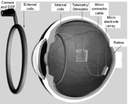
Recently, owing to integrated circuit technology progress and innovations in circuit design techniques, more and more systems can be fabricated in a single chip (SOC) that make integrated biomedical device smaller and have possibility to be implanted to supplement, or even entirely replace biomedical operation. Several implantable microelectronic systems already exist [1] (Fig. 1.1): pacemakers are used to replace a defective natural cardiac pacemaker [2] (Fig. 1.2), cochlear prostheses are used to help provide a sense of sound to a person who is partially or profoundly deaf, visual prostheses are used to restore eyesight to the blind [3] (Fig. 1.3) and neural recording and stimulation systems are used to treat patients with Parkinson‟s disease and epilepsy [4]. This thesis focuses on neural recording and stimulation systems‟ power supply design. Fig. 1.4 is the overall system‟s architecture. The mainly function of this system divide into two part. The first part is amplifying the neural signal by amplifier, then converting the analog signal to digital signal and then transmits the information through the RF circuit. The second part is use DSP to analyze the digital signal and then use analyzed result to determine whether the patient needs stimulating.
Since biomedical device need to implant into the human body and implanted medical device are vital to the patients, the implantable medical device most have a long term reliable power supply for implanted medical device. However, currently battery technology cannot stand for an enough time even for small power
consumption implanted pacemaker [5]. Therefore, wireless power transmit to medical device must be considered. Several possible wireless power transmission method are summarize in table 1.1 [6] [7] [8] [9] [10]. Depend on different power consumption on implanted medical device, different wireless power transmission method would be adopted. Since neural recording and stimulation systems power consumption may up to ten mW, thermoelectric and far-field electromagnetic energy transfer methods which still cannot offer such power level on recent research would not be a proper method for wireless power transmission. Secondly, because neural recording and stimulation systems need to implant into human brain on a fix position to sense the neural signal and stimulate human brain, it may unsuitable use vibration and heel strike to generate power from human motion or walking. Third, transmission efficiency should be high to avoid excess human exposure to electromagnetic wave, therefore optical recharging which power transmission efficiency is poor would not be a good candidate. Summarizing above reason, near field inductive link power supply become most widely use method to power the implanted device from medium power level to high power level [1].
Near-field inductive link power supply majorly can divide three different parts: near field coil, rectifier and regulator (Fig. 1.5). For near field coil design, coil‟s size which be confined by the implanted physical size in human body is an important design factor that mainly determined the power efficiency and the transmission distance. However, operating frequency, structure of coil and inductance value also have impact on transmission efficiency. Designer must carefully trade off the above factors to make a high efficiency transmission. For rectifier part, passive and off chip schlocky barrier diode used to be a suitable choice to implement [9]. However, the off chip schlocky barrier diode have large dropout voltage 0.3V, which will result large power consumption especially in low voltage high current system of the neuron
recording and stimulating and the off chip schlocky barrier diode cannot integrate with other circuit. The first on chip rectifier was proposed [11]. Then more and more on chip active rectifiers have been developed [12] [13]. The on chip active rectifiers using four switching power mos which can effective reduce the dropout voltage when current conduct. The experiments verify that the new on chip rectifier not only have better AC to DC conversion efficiency, but also have smaller area and suitability for system integration. After the rectifier converse the AC power into DC power, the regulator need to connect the rectifier output since the voltage output voltage of rectifier is really noisy. For regulator part, high efficiency low dropout regulator is the most choice for most biomedical system. However, since high resolution and multi channel simultaneous neuron signal sensing application need, the noise of power supply for analog circuit like pre-amp and analog to digital conversion must be less than before works.
1.2 Motivations and Main Result
In CMOS active rectifier, the proposed comparator circuits compensate both turn-on and turn-off delays and make active rectifier operated at a higher frequency, (FCC approved ISM band13.56 MHz) than that in the previous work (1.5MHz)[14]. Since the large power transistor delay is compensated by the proposed comparator circuits, the larger output current (20 mA) than that in the previous work (2mA)[13] can be achieved for implantable epilepsy detection and stimulation applications. The deep n-well parasitic diodes of power NMOS and additional start control circuit make the active rectifier start up robustly. The fabricated CMOS active rectifier can be operated at high frequency (13.56MHz) and deliver 20mA output current while maintaining the power conversion efficiency of 84.8% and provide low output peak-to-peak ripple (14mV) than those in the previous works(≈100 mV [14], ≈ 200mV[13]). In CMOS LDO regulator, the fabricated CMOS LDO regulator has
-58.49dB PSR up to 10MHz that better than previous work (-40dB at 1MHz)[36] [18]. The fabricated CMOS LDO regulator deliver 20mA output current while maintaining the lower dropout voltage (200mV) than the previous work (600mV) [18]. The single dominant pole compensation [28] of LDO regulator consumes the higher quiescent current 98uA than previous work [36][19] when deliver the same amount of output current. The additional ESR zero can be avoided. This makes LDO regulator have the smaller transient load regulation of 5.75mV than that in the previous work (15mV)[19] when the load current rises from 0mA to 20mA in 10ns. In the inductive link power supply, the fabricated inductive link power supply has a lower peak-to-peak output ripple of 11.5mV and higher power conversion efficiency of 76.3% than those in the previous work(80mV, 75.6%)[35].
1.3 Thesis Organization
In chapter 1, the background has been introduce in section 1.1, including the different purpose biomedical devices, the neural recording and stimulation system‟s overall architecture, the distinct wireless power transmission methods and the overall near-field inductive link system architecture. Then the motivation and main result of this work are proposed in section 1.2. The section 1.3 is thesis organization.
In chapter 2, the whole system and the individual blocks design would be discussed detailed. In section 2.1, the whole system design consideration would be discussed. In section 2.2, the efficiency optimum equation derivation, coil structure design and the IEEE safe limit to human exposure computing method would be described. In section 2.3, the rectifier transistor level operation, the start-up mechanism, the latch-up consideration and the new proposed delay compensated comparator operation would be described detail. In section 2.4, the stability, the compensation methods, transient load regulation and the high PSR technique of low dropout regulator would be discussed.
In chapter 3, the whole chip layout consideration would be described in section 3.1. In section 3.2, the chip performance measurement setup would be described. In section 3.3, the experiment results of each blocks and whole chip would be demonstrated. In section 3.4, the whole chip experiment results and each blocks experiment results will compare with other recent research results and discuss the distinct circuit design techniques.
In chapter 4, the results of the near-field inductive link power supply of this work would be summarized. Furthermore, the chapter ends also discuss about the possibility of improvement to the future near-field inductive link power supply design.
Energy source Power density efficiency distance implant Thermoelectric [7] 20uW / cm2 N.A. N.A. YES
Optical recharging
[8] 4.4mW / cm
2 20% 2mm YES
Vibration
(human motion) 4uW / cm
3 N.A. N.A. NO
Heel strike (walking) 10-700mW N.A. N.A. NO Near-field inductive energy transfer [9] 140 mW / cm 2 75% 7mm YES Far-field electromagnetic energy transfer [10] 3.5 mW / cm2 0.08% 1.75cm YES
Table 1.1 Power sources options
Figure 1.2 the visual prostheses are used to restore eyesight to the blind.
Figure 1.3 the overall system‟s architecture of neural recording and neuron stimulator. The system is fully power by wireless inductive link.
CHAPTER 2
SYSTEM DESIGN AND SIMULATION
In this chapter, the near-field inductive coils, the on chip active rectifiers and low-dropout regulator will be discussed in section 2.1, 2.2 and 2.3 respectively. In section 2.4, the whole chip architecture and design consideration will be mentioned. In section 2.5, the post-simulation of the individual blocks and whole chip will be described.
2.1 Near-field coil
For near field coil design, coils‟ size which be confined by the implanted physical size in human body is an important design factor that mainly determined the power efficiency and the transmission distance. However, operating frequency, structure of coils and inductance values also have impact on transmission efficiency. Designer must carefully consider the trade off on the above factors to make a high efficiency transmission. The following sub-section will derive the coils‟ efficiency equation; describe the coils‟ design flow and calculate the human exposure to EM field.
2.1.1 Transmission Efficiency Analysis
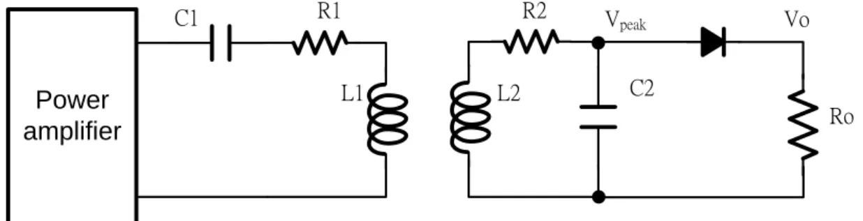
The fundamental inductive powering circuit is show in Fig. 2.1 [20]. The primary part use series resonance capacitor instead of parallel resonance capacitor for matching needy. The diode voltage conversion is define to be A = Vo / Vpk, where Vpk
dropout voltage is much smaller than Vpk and RoCo >> 1 / f , then A ≒ 1 and Vpk ≒
Vdiode. The equivalent ac load resistance Rac which will dissipate an amount of a.c.
power equivalent to the d.c. power in Ro is:
(2.1)
The equivalent ac parallel resistance can be transform into equivalent ac series resistance [21]:
(2.2)
The w is the radian frequency 2πf. The Fig. 2.2 is the equivalent circuit of secondary part. The total equivalent series resistance in secondary tank circuit is R2+RL, where
R2 is the parasitic series resistance of the inductor.
The equivalent resistance Re, reflected back into the primary coil, is:
(2.3)
where is the mutual inductance of the coils and Q1 = wL1 / R1 and Q2
= wL2 / R2 are the unloaded Qs of the primary and secondary coils respectively. From the primary equivalent circuit, show in Fig. 2.3, the circuit efficiency at resonance can be determined:
(2.4) and
(2.5) and
(2.6)
In inductive link wireless power, the maximum value of k is determined by coil size and spacing. For maximum efficiency d η / d R2 equals zero, thus:
(2.7)
Substituting equation 5 into equation 4, the optimum efficiency of the circuits is given by
(2.8)
Equation above indicates that optimum efficiency ηopt, increases as k2Q1Q2 increases,
which is the same conclusion with recent research [22]. However, the coils‟ Q is limited, since coils tend to have great Q when coils‟ sizes which be limited by implant body size become large. Therefore, we design the coils must have the highest unloaded Q and k in a small space to achieve the efficiency wireless power transmission.
2.1.2 Near-Field Coils Design
Once the system application decide the implant physical size constrain, the coupling coefficient (k) can be maximize by proper choosing the outer diameter size of coils, and the Q factor can be maximize by proper choosing the coils‟ structure and coils‟ material. Since Q factor and coupling coefficient are increase as the outer diameter increase, the first step of efficient near-field coils design maximizing the coupling coefficient would not conflict the design parameter of maximizing the Q factor. Once we maximize the coupling coefficient by deciding the primary and secondary coils‟ outer diameter, that recent research have been widely studied [23] (Fig. 2.4, Fig. 2.5), we can maximize the Q factor by using allowable wide copper metal and low loss coil structure. The coil structure mainly divides into three parts: multi layer cylindrical coil (Fig. 2.6), single layer cylindrical coil (Fig. 2.7) and spiral coil (Fig. 2.8). The different structure have different Q factor, because the skin effect
and the proximity effect [24].
Skin effect is usually described as the tendency of current to flow primarily on the surface (skin) of a conductor as frequency increases. Because the inner regions of a conductor are thus less effective at carrying current than at low frequencies, the useful cross-sectional area of a conductor is reduced, thereby producing a corresponding increase in resistance (Fig. 2.9) [21].
Proximity effect is a phenomenon of current crowding at a surface of a conductor because of current flowing in a nearby conductor. The reason of current crowding at a surface of conductor is the nearby conductor current flow constructs magnetic field and makes a perpendicular force to the moving electron in the conductor. When electrons crow at a surface of a conductor, the effective resistance increases (Fig. 2.10) [21].
Summarizing above physics phenomenon, the single layer cylindrical coil have the greater Q factor than multi layer cylindrical coil and spiral coil. The reasons are the multi layer cylindrical coils have worse proximity effect than single layer since its second layer conductor overlap the first layer, and the spiral coil wind conductor circle smaller and smaller since a smaller circle have smaller Q factor than a bigger circle. However, the single layer cylindrical coils have the largest size for a particular inductance. Therefore, secondary part coil is not suitable using single layer cylindrical coils since it‟s too thick. The spiral coil is the better option for secondary coils, because spiral coil so thin that make coil implant into human body possible. For primary part, it have different consideration to secondary part. The coil on the primary part is outside the body and coils‟ thickness would not be a big problem, so single layer cylindrical coil would be a good option.
After decided the coil structure, the conductor material must be properly selected. Since effective series resistance of coils needs to be decrease to achieve high quality
factor (Q), the conductor must have high electrical conductivity. If cost doesn‟t consider, silver would be the best option since silver have the highest conductivity. Copper conductor coat with silver were be the second option which use a little silver to decrease the surface resistance of conductor. Since electrons tend to gather on the conductor surface, this approach may be a good option. The cheapest and widely adopting option is simply using solid copper conductor. There are also have many previous researches using litz-wire to make low resistance conductor [9] (Fig. 2.11). The litz wire is a wire which composes by many thin wires. Since electrons move on the conductor surface, litz wire can increase the surface area. However, when operating frequency increase further (above 2MHz), irregularities in stranding and capacity between the individual strands result in failure to realize the ideal conditions in litz conductor [24][25]. Therefore, the biomedical inductive link which must operate in ISM band (6.78MHz or 13.56MHz) is not suitable using litz wire as the coils‟ conductor.
After maximize coupling coefficient and Q factor, input resistance matching and optimizing R2 value are the next step. The R2 value and input resistance can be adjusted by change winding turns on primary and secondary coils. First, the R2 value increases as winding turns increase since wire become longer. Once we decide the R2 value, secondary coil inductance value can be decided, because Q factor (wL2 / R2) have unremarkable dependence on coil winging turns. After R2 optimizing, input resistance can be tuned. The input resistance is Re+R1 which also increase as winding turns increase. The primary coils‟ Q factor (Q1) also has unremarkable dependence on coil winding turns. If power amplifier output resistance is 50 ohm, then we can use below equation to decide the R1 value:
(2.10)
Since ac equivalent loading (Rac), coupling coefficient (k), quality factor (Q1, Q2) and secondary coil effective resistance (R2) are not depend on primary coil winding turns, we can adjust the primary coil winding turns to increase or decrease R1 value that makes input resistance equal to 50 ohm without changing other parameters. Once R1 value is decided, the L1 value also is decided since Q1 factor unchanged remarkable. After the last step of input resistance matching, the near-field coils can efficient transmit wireless power from primary to secondary.
Summarizing all above design consideration, we can derive an efficient coil design flow for neural recording and stimulation systems.
1. Decide the size constrains and transmission distance for implant condition. For neural recording and stimulation systems, implant size cannot excesses 2cm diameter, thick 0.5cm and transmission distance is about 0.6cm to 1cm. 2. Maximize the coupling coefficient (k) through Figure 2.5.
Select z = 1cm, doutR = 1.5cm and doutT = 4cm result coupling coefficient =0.11. (Since dinT and dinR are not remarkable influence coupling coefficient, we reserve these variables for Q factor maximize and R2
optimum.)
3. Maximize the coil quality factor (Q).
Use single layer cylindrical coil for transmit coil instead of the spiral coil. (AWG = 18, Q about 160)
Use conductor in receive coil as wide as possible under size constrain. (AWG = 25, Q about 100)
Before calculating ac parallel equivalent resistance, the rectifier electrical performance and system power consumption (after rectifier) need to be ready. Since the active rectifier (which is the most efficient rectifier in recent research) has AC to DC 85% efficiency and dropout voltage 0.3v, the system power consumption need 40mW (2V, 20mA), we can calculate the Rac by
following step: (2.11) (2.12) (2.13) (2.14) (2.15)
Once R1 value is decided, L1 value would be decided and can be measured by experiment.
5. Calculate and connect the needy resonance capacitor (Cres) to the primary and
secondary coils.
Since coils have parasitic capacitance, resonance capacitors which need connecting to the coils must minus the parasitic capacitance from total capacitance.
(2.16)
(2.17)
The Cparasitic value can be obtained by measurement.
When 13.56MHz sine waves transmit from primary coil to secondary coil, the magnetic field variation generator by primary coil would heat the human skin [26]. Since high temperature on human skin may damage the human cell, magnetic field should be low enough such that heat would not cause any damage on human body. The roughly calculate to power dissipation on human skin can be showed below [27]:
(2.18) Then magnetic fields generator by primary coil is:
(2.19)
Then electric fields induce by magnetic field on skin is: (2.20)
Then the power loss due to skin absorption can be calculated: (2.21)
(2.20)
2.2 CMOS Active Rectifier
2.2.1 Active Rectifier Operation
The conceptual circuit of the proposed rectifier is show in Fig. 2.12 [14]. The input sine wave voltage is generated from the inductive link receiver coil. The pMOS power transistors Mp1, Mp2 form a cross-coupled pair such that both Mp1 and Mp2 function as switches with only a small |Vdrop, p| drop when either of
them is turned on. In addition, a 2-terminal comparator CMP1 (CMP2) controls the switching of nmos power transistor Mn1 (Mn2) by comparing voltage Vin1 (Vin2) with ground potential. Transistor Mn1 (Mn2) will only be turned on when the voltage Vin1 (Vin2) < 0 V to maintain the unidirectional charging current flow. The Mn1
(Mn2) operates in the linear region as a switch with small Vdrop, n drop during
conduction. As a result, the active rectifier voltage conversion ratio can be derived as: (2.21)
In addition, the active rectifier power conversion efficiency can be roughly showed below:
(2.22)
Where Vdo is the total voltage drop when power mos turns on. Iin is the total input
current. Iout is the output current to the smoothing capacitor. Iloss is total current loss
include: reverse leakage current which would happen when power mos turn off delay, comparator power consumption and buffer power consumption.
The active rectifier steady-state operation method is illustrated in Fig. 2.13. The operation steps can be divided into three steps during the negative half cycle (Vin=Vc1-Vc2). During Sa period, 0V < Vin < |Vthp| and 0 < Vc1 < Vc2 < Vout, Mp2
is cutoff. Since Vc1 > 0, comparator would not turn on Mn1 and no current would flow through Mn2. When input voltage Vin goes up till Vin > |Vthp|, rectifier enters
step Sb, Mp2 is turned on and Vout node short to Vc2 node. Therefore, Vc1 = Vout –
Vin, Vin increase further would make Vc1 voltage decrease since Vout is a stable voltage in steady state. In addition, Vc1 is still lager than ground, therefore comparator still output low and turn off the Mn1. Since Mn1 is off, no current will flow through Mn1, I1 = I2 = I3 = 0. As input voltage increase further, then Vc1 voltage
decrease further. When Vc1 < 0, rectifier goes into step Sc, comparator output high
and turn on the Mn1. Since both Mp2 and Mn1 turn on, charging current will flow from Vin to Vrec and charge the smoothing capacitor to the voltage Vin - |Vdrop, p| -
Vdrop, n. Since both Mp2 and Mn1 operate in triode region, the large power mos size of
and Vdrop, n. Therefore, voltage conversion ratio is maximized since |Vdrop, p| and Vdrop, n
are minimized. When the voltage Vin reach the peak value, Vin voltage starts to decrease. When Vin decrease to |Vthp| < Vin < Vrec, rectifier re-goes into Sb step. In Sb
step, the power mos Mn1 turn off and no current flow through Mp2 even Mp2 is still on. When Vin voltage increase further Vin < |Vthp|, Mp2 turn off and rectifier go into
Sa step. The negative voltage half cycle is finished till Vin = Vc2 –Vc1 = 0 and the
next cycle repeat the step that illustrate above. However, the power mos involve the positive cycle are Mp1 and Mn2 instead of Mp2 and Mn1.
2.2.2 Delay Compensated Comparator
In steady state operation of active rectifier, the time of power mos turn on and turn off would not perfect match the time of Vc1 = 0 (Vc2=0, for another half cycle). The reason is the comparator and the buffer have to charge and discharge the large gate capacitance of the power mos. The gate capacitances of Mn1 and Mn2 large are due to the large size of Mn1 and Mn2. However, Mn1 and Mn2 need using large size mos to decrease the conduction dropout, maximize the conversion efficiency and suite for low voltage high current application in neuron recording and stimulating. The large gate capacitance result in large signal delay even buffer is added after comparator. Therefore, the delay time of Mn1 and Mn2 turn-on and turn-off would not perfect match the time of Vc1 = 0 (Vc2=0, for another half cycle). The delay of the time of Mn1 and Mn2 turn on and turn off would decrease the rectifier power conversion efficiency. The delay of the turn off time happen on rectifier step transition from Sc back to Sb, Mn1 (Mn2) should be turned off when Vin1 increases to 0 V.
However, the delay of Cmp2 to discharge the large gate capacitance of Mn1 (Mn2) cannot allow Mn1 (Mn2) to respond instantly. Therefore, when Vin decrease and Vin1 (Vin2) > 0, power mos Mn1 (Mn2) still is turned on. The reverse leakage current
would flow from the smoothing capacitor C0 back to the rectifier. The reverse leakage current make rectifier power conversion efficiency decrease since Iloss increases in
equation (2.22). On the other hand, the delay of the turn on time also decreases power conversion efficiency since conduction time decrease. This phenomenon would become important if the active rectifier operate in the ISM band (13.56MHz). The rectifier operates in higher frequency the useful conduction time for each cycle would be less. Therefore, the turn-on delay would shrink the conduction time about half or more which serious decrease the power conversion efficiency on rectifier.
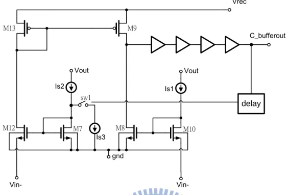
In this active rectifier, we propose a new delay compensated comparator to solve not only the turn off delay problem [13] [14], but also the turn on delay problem. The overall circuit diagram is show in Fig. 2.14. The delay compensated comparator consist by a pair of common gate amplifier CGA1 (M8, M10) and CGA2 (M7, M12), a current mirror (M13, M9), and four stage buffer to drive large gate capacitance of nMOS power transistor in the rectifier. In the proposed comparator, CGA2 with the current mirror and CGA1 realize a push pull output stage in order to decrease the charge and discharge time of the output stage even under the low quiescent current. As a result, the delay time of the comparator can be minimized.
In addition, the proposed delay compensated comparator is realized by three unbalanced-biasing schemes (Is1, Is2 and Is3) such that comparator have controllable input offset voltage which canceling the time of turn on and turn off delay. The overall rectifier circuit with input offset cancellation is show in Fig. 2.15. When the comparators have input positive offset, the comparators can turn on when Vc1 ≦ Vos instead of Vc1 ≦ 0V. Therefore, comparator would turn on early and cancelling the time of charging large gate capacitance delay. When the comparator output high, the negative feedback in the comparator would change the input positive offset into input negative offset and turn off power transistor on Vc1 ≧ Vos instead of the time of Vc1
≧ 0V. Therefore, the comparators would turn off early and cancelling the time of discharging large gate capacitance delay. The illustrate waveforms of positive half cycle is show in Figure 2.16.
Region Ⅰ: |Vtp| < Vac(Vc2 - Vc1) < Vrec - Vosp, Mp2 on, Mp1 off, Vc2 = Vrec, Vg,Mn2 = 0, Mn2 off, Vc1 = Vrec – Vac > Vosp, Vg,Mn1 = 0, Mn1 off, no charging current.
Region Ⅱ: Vrec – Vosp < Vac < Vp, Vc2 ≥ Vrec, Vg,Mn2 = 0, Mn2 off, Vc1 = Vrec -Vac < Vosp, Mp2 on, Mp1 off, cmp1 output high, Vcmp1= Vout, Vg,Mn1 = Vrec, Mn1 turn on at Vac ≈ Vrec after the turn-on delay, Vac charges Co, Vc2 > Vrec, Vosp → Vosn after the delay of inverter delay block for Mn1 on.
Region Ⅲ: Vrec + Vosn < Vac < Vp, Vc2 > Vrec, Mp2 on, Mp1 off, Vg,Mn2 = 0, Mn2 off, Vc1 = Vc2 - Vac < -Vosn, cmp1 output high,Vcmp1= Vout, Vg,Mn1 = Vrec, Mn1 on, Vac charges Co.
Region Ⅳ: |Vtp| < Vac < Vrec + Vosn, Mp2 on, Mp1 off, Vc1 = Vrec - Vac > -Vosn, cmp1 output low,Vcmp1= 0, Vg,Mn1 = 0, Mn1 turn off at Vac ≈ Vrec after the turn-off delay, Vac stop charging Co, Vc2 = Vrec, Vosn → Vosp after the delay of inverter delay block for Mn1 off.
Region Ⅴ: 0 < Vac < |Vtp|, Mp2 off, Mp1 off, |Vtp| < Vc2 < Vrec, |Vtp| < Vc1 < Vrec, Mn1 off, Mn2 off, no charging current.
The input offset control mechanism of the delay compensated comparator is described below. Since two common gate amplifiers (M8, M10, M7 and M12) bias in saturation region and have the below equation:
(2.23)
where (W/L) is the transistors M7, M8, M10, and M12. The comparator input offset can be derived by following equation:
(2.24) (2.25) Then equation (2.24) minus (2.25):
(2.26)
Therefore, when power mos is turn off, the switch which in comparator is also off since switch is synchronization with power mos. The current flow through M7 would be Is2 and the current flow through M10 would be Is1. Since we design Is2 > Is1, the comparator would have input positive offset voltage equal to (2.26), that would make comparator turn on early and cancelling the turn on delay. Once the power mos is turn on, the switch is also turn on, and the current flow through M7 would become Is2 – Is3. Since we design Is2 – Is3 is smaller than Is1, the input offset become negative and ready to turn off power mos early to cancel the power mos turn off delay. Owing to double side input offset control, the rectifier with this comparator can operate up to 13.56MHz since high frequency operation have serious delay problem. The supply voltage of the comparator connects to the LDO regulator output voltage Vout to avoid
the noisy active rectifier output voltage Vrec. The following level converter would
convert the lower swing of the comparator output voltage Vcmp1 to the higher swing
voltage VLC2 to drive the power MOS.
2.2.3 Start-up Mechanism and Latch-Up Consideration
When the implant device is not in use and turned off, both the input and the output voltages of the rectifier are at 0 V (Vrec = 0 V), as no signal is transmitted from the external coil to the implant coil. It is crucial for the rectifier to be able self start-up since there is no power supply in implant device.
terminals of transistor Mp1, any increase in Vin will increase gate to source voltage of Mp2. Transistor Mp1 will be turn on to give rise to Vin = Vout = 0 V and Vc1 = -Vin when Vin is larger than the turn-on threshold of transistor Mp1. In addition, when Vc1 = -Vin, the transistors M10 and M12 in the proposed comparator are on, as Vin is larger than their threshold voltage. This condition will lead to transistors M8 and M9 in cutoff and linear region respectively and input voltage of the inverter chain (buffer) is 0 V. Therefore, the power transistor Mn1 gate voltage is determined by parasitic capacitor network since inverter chain is cutoff [14]. The value of Vg, Mn1 is a
capacitive ratio of Vc1 as:
(2.27)
Therefore, when Vc1 decrease further, the difference between and Vc1 get larger. Transistor Mn1 will then be turned on when the voltage difference is larger than its threshold voltage. Therefore, current will flow from rectifier input to rectifier output through Mn1 and Mp2 to charge the output voltage smoothing capacitor such that rectifier output voltage increases. Moreover, when Vc1 is decrease further, the parasitic diode (D1) of power mos Mn1 will also conduct the charging current to rectifier output. Therefore, rectifiers can start-up by self even when rectifier output (Vrec) is zero voltage.
Since the proposed rectifiers have used body diode to conduct current when rectifier output is zero, the latch-up risk is rising. However, when current conduct through Mp2, the body diode of Mp2 would not turn on since power mos size is designed high enough such that conduction drop is 150mV maximum. Since latch-up happen when two parasitic BJT of nmos and pmos form a positive feedback [28], the cutoff parasitic BJT of pmos break the positive feedback and make latch-up impossible. Moreover, the nmos body can use deep N-Well to isolate the P-Well and P
substrate. Therefore, the charging current will flow through the P-Well to N+ region (nmos drain terminal) since nmos drain terminal connect to Vc1 and Vc1 < -Vthn (Fig.
2.17). Since the P substrate will no current flow through it, the latch-up risk can also be released.
2.3 Low-dropout Regulator
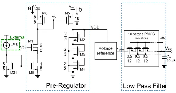
For regulator design, the system specifications that power consumption, current transient and allowable supply variation often are conflicting. The task of maximizing load regulation, maintaining stability, and minimizing transient output voltage variation prove to be challenging. This work focuses on high PSR, low power consumption and low transient load regulation for implant device. The figure 2.18 is the whole system architecture of regulator. The system is composed of a pre-regulator, a voltage reference, a low pass filter and a low dropout regulator. Since the LDO regulator focus on brain implant medical device, the temperature of the chip would maintain about 37˚C. Since the M1 and M3 operate in sub-threshold region, the small quiescent current and the low power supply voltage requirement of the voltage reference can be achieve. The low power supply voltage requirement of the voltage reference is suitable the cascoded pre-regulator. [29] (Fig. 2.19).
2.3.1 Stability and Compensation Method
The figure 2.20 is the system architecture of low dropout regulator. The system is composed of an error amplifier, an output capacitance, a feedback resistor network and a pass element. Because the low dropout regulator is a negative feedback system, the stability issue should be concerned [30] [31]. The figure 2.21 is the ac small-signal block diagram of the proposed LDO regulator that illustrates the intrinsic factors that
determine the stability of the system, namely, an error amplifier, a pass element, feedback resistors, effective output impedance, and an output capacitor and associated ESR. For the purpose of analysis, the feedback loop can be broken at “A” in figure 2.22. It is readily apparent that the system must be unity gain stable, considering Tin
and Tout to be the input and the output voltages respectively. The open-loop transfer
function can be described as:
(2.28)
where gma and gmp refer to the transconductance of the amplifier and the pass
element, Roa is the output impedance of the amplifier, Cpar refers to the parasitic
capacitance introduced by the pass element, C1 is the input capacitance of the buffer and Z is the impedance seen at Vout:
(2.29)
where Co and RESR are the capacitance and the effective series resistance of the output
capacitor. Since R1 and R2 always are large to keep the quiescent current low, the Z impedance can be simplified further:
(2.30)
Since Rpass is always much larger than RESR, the impedance Z can be simplified
again:
(2.31)
It can be observe from equation (2.28) and (2.31) that the overall transfer function of the system consist of three pole and on zero, a potentially unstable system.
(2.32) (2.33)
(2.34) (2.35)
The Z1 is a left half plane zero which many works on regulator using this zero to improve the open loop gain transfer function [30] [31]. However, since this work focus on implant device power supply design, the variation on RESR may cause system
unstable and damage the patient. Therefore, select a high frequency capacitor which has low RESR as an output capacitor. Since C1 and RESR are small, the P3 and Z1 are
seen at much higher frequency than P1 and P2. Therefore, one dominates pole
compensation as a compensation method for implant application is preferable. Then, Co select large that make P1 be a dominate pole and make system feedback loop stable. Therefore, the typical frequency response can be show on the figure 2.22. When load current of the implant device is increase, the pole1‟s will frequency increase and DC gain is decrease lightly since Rpass decrease linearly with increasing
current and transconductance of pass element only decrease with root of current. When the pole1‟s frequency increases, the LDO regulator unit gain frequency also increase. The increased unit gain frequency may cause system unstable since pole3 become smaller than unit gain frequency. Therefore, the LDO regulator should have enough phase margin when system is high load current.
2.3.2 Transient Load Regulation
An important specification is the maximum allowable output voltage change for a full range transient load-current step [30] [31]. The application determines how low this value is required to be. Figure 2.23 is the transient load regulation of the LDO under a sudden load current step change. The time require for the loop to respond (Δt1,
maximum load-current, and maximum allowable output voltage variation. However, the internal slew-rate associated with the parasitic capacitance (Cpar) of the pass element. The resulting time can be approximated to be:
(2.36)
where BWcl is the closed-loop bandwidth, tsr is slew rate associated with Cpar, ΔV is
the voltage variation at Cpar, and Isr is the slew-rate limited current. However, if the
slew-rate current is large enough, the reciprocal of the closed-loop bandwidth starts to dominate theΔt1. This would be at the cost of quiescent current. The worst case time
required for the loop to respond is specified by the maximum permissible output voltage variation (ΔVtr), which is a function of the output capacitor (Co), the effective
series resistance (RESR) of the output capacitor, the bypass capacitors (Cb), and the
maximum load current (Iload-max),
where is the voltage variation resulting from the presence of the ESR of the output capacitor. Since this work have not used ESR zero compensation, the ESR is really small and can be neglected.
Once the slew rate condition is terminates, the output voltage recovers and settles to its final value. The final value will have a drop:
where is the closed loop output impedance of the regulator. This is essentially the effect of load regulation performance. The settling time (Δt2) is dependent on the
time required for the pass element to fully charge the load capacitors and the phase margin of the open-loop frequency response.
When load current step from full scale to zero, the output voltage variation ( ), whose magnitude is defined by the voltage charged on the capacitors and the voltage
generated across the ESR of the output capacitor. Then the transient voltage variation can be approximately expressed as
Since the RESR value in this design is really small, the ESR voltage drop can be
neglect. Then the transient voltage variation can be:
Finally when the output transistor is shut off (after ) the output voltage takes time to discharge to its final ideal value:
Since R1 value is typical large to decrease the quiescent current, the pull down current
will be low. Therefore, the tradeoff between quiescent current and the pull down current for regulator design must be carefully consideration.
2.3.3 High PSR Technique
Since LDO regulator needs to stable the voltage variation come from rectifier, the LDO regulator must have high PSR performance to eliminate the supply noise on the output. The basic LDO PSR analysis was derived [19]. The finite PSR of the conventional LDO is due to several paths between the input and output of the LDO. Figure 2.24 shows the various paths that could couple input ripples to the output of the LDO. Path 1 is the main path regulated by the LDO loop. Path 2 is caused by the finite conductance of the MOS pass transistor, Mp, and it is more significant for
technologies with lower feature sizes. Path 3 is as a result of the finite power supply rejection ratio (PSRR) of the error amplifier, and finally path 4 is due to the finite PSR of the voltage reference circuit. The LDO transfer function due to paths 1 and 2 is given by:
where gm and ro are the transconductance and channel resistance of the pass element,
Mp. ZL is the total load impedance (without feedback resistances Rf1 and Rf2 ) that
appear at node Vout, and Aeo and ωe are the DC gain and dominant pole of the error
amplifier, respectively. Equation (1) shows that PSR depends on feed-back gain (Aeo Rf2 /(Rf1+ Rf2)) at lower frequency. As the frequency increases, the dominant pole
of the error amplifier reduces the feedback gain. Therefore, the PSR due to path 1 and 2 starts to degrade and ripples at the output may get amplified at high frequencies. The upper and lower limits of PSR due to path 1 and 2 are given by
For path 3 and 4, the transfer function is given by:
where PSRRe is the power supply rejection ratio of the error amplifier, and PSRBG is
the power supply rejection of the voltage reference circuit. To understand path 3 and 4 further, the transfer function of path 3 and 4 can be derived below:
positive in the proposed analysis [19], since error amplifier‟s supply and output node always connect to source or drain terminal of mosfet that make the phase the same. At higher frequencies due to dominant pole of error amplifier the power supply ripple can only be decoupling by
However, when we consider the ESL effect, the impedance would not goes to zero. Hence the error amplifier and voltage reference noise contribute to the output directly.
To solve the above problem, the pre-regulator is added in front of voltage reference supply (Figure 2.18). The pre-regulator is show in figure 2.25. Since the impedance that Vrec seen into the M6 source is , and the M6 drain seen a high impedance . Therefore, the noise come from Vrec is replicate on M6 gate terminal since . Further, the M5 transistor that operates in saturation region the source and gate terminal sense the same phase and the same amplitude noise that come from Vrec. Therefore, the noise will cancel each other in drain terminal of M5. The PSR of the voltage reference circuit is improved. Further, the RC low pass filter is added after the voltage reference circuit to eliminate the high frequency noise contributes to LDO core (Figure 2.18). Since voltage reference output connects to LDO core‟s differential input gate terminal, there is no current flow between the LDO and voltage reference in steady state. Therefore, use high resistor to achieve low frequency corner would not induce large power consumption. Owing to above circuit, the path 4 supply noise can be eliminated and the equation becomes:
and 3. Since path 3 supply noise is negative contribution of Vout node and path 1 and 2 supply noise is positive contribution of Vout node, supply noise can cancel each other on the Vout node if path 3 transfer function gain equal to path 1 and 2 transfer function gain. Therefore, if we design error amplifier have poor PSRe which equal to
1, then equation can be derived below:
where supply noise transfer function of path 3 is equal to path 1 and 2. Therefore, the high PSR LDO core can be achieved. In the higher frequency, the path 3 transfer function can be derived below:
where supply noise transfer function of path 3 is also equal to path 1 and 2. Therefore, LDO core will have high PSR in the low and high frequency independent on error amplifier‟s gain and the conclusion is different to [19]. Actually, increase the PSRe
can reduce the regulator‟s PSR at the same error amplifier‟s gain. However, the above theory derivations assume PSRe(s) always equal to 1 in any frequency. In actually, the
PSRe(s) will degrade when frequency above the PSR(s) dominant pole. Therefore, the
PSR of LDO core cannot up to infinite frequency.
To achieve PSRe(s) = 1, we propose a new supply noise tracking architecture to
improve the PSR performance without conduct a large quiescent current. The figure 2.26 is circuit diagram of the LDO without voltage reference. When the impedance that Vrec seen into the M3 source is , and the M17 drain seen a high impedance . Therefore, the noise come from Vrec is replicate on M7 gate terminal since . Further, the M7 transistor that operates in saturation region the source and gate terminal sense the same phase and the same amplitude noise that come from Vrec. Therefore, the noise will cancel each other in drain
terminal of M7. However, when considerate the channel length effect, there is supply noise also pass by ro (output resistance of M7) and the M16 drain also seen a high
impedance . Therefore, the noise come from Vrec is replicate on M5 gate terminal since too. Then supply noise pass to M5 gate to source with the same phase since M5 is a source follower. Therefore, PSRe(S) = 1 is achieved
on error amplifier‟s output. However, large parasitic capacitance of Mp1 forms a pole that degrades the supply noise on the gate of Mp1 at high frequency. Therefore, the LDO core‟s PSR bandwidth would not be infinite. Even through, the finally design of regulator (figure 2.27) can achieve PSR -60dB from 0 to 1MHz and -50dB to 10MHz.
2.4 Whole Chip Design Consideration
The conventional whole chip diagram is show in figure 1.5. However, when the new proposed high efficiency active rectifier implement in this architecture, the wrong operation may occur on active rectifier. Since the receive coil need to deliver large current for the implant device and receive coil driving ability is limited, the Vrec voltage would not rising instantly. Therefore, the low voltage Vrec which use to supply the comparator power in active rectifier would cause comparator having serious turn on and turn off delay. When comparator delay is too large, the leakage current flows from smoothing capacitor back to receive coil such that Vrec voltage keep at low voltage and does not increase further. Therefore, we proposed a new whole chip architecture that show in figure 2.28. In the proposed architecture, the comparator use LDO output as power supply instead of rectifier out. The LDO out is always stable at 1.8V make comparator would not sensitive to power supply anymore. In addition, the start-up control circuit senses the LDO output voltage to decide to turn on or turn off the comparator. If LDO output voltage > 1.2V, start-up control
circuit will turn on the comparator and rectifier enter into switching mode (Fig. 2.29). The detail circuit of the startup circuit is show in figure 2.30.
In the figure 2.28, the comparator output driver is using Vrec voltage as the power
supply. The reason is that Vrec voltage is higher than Vout voltage such that drivier can
provide higher driving ability to power mos and reduce the power mos resistance. In addition, the driver circuit is composed by a chain of inverter that will cause transient noise. Therefore, if the driver circuit connects to the Vout node, the noise will
contribute to the Vout node and make implant noisy. However, Vrec and Vout are different voltage; the power supply for driver change from one another must using a level converter, which is show in figure 2.31.
2.5 Simulation Results
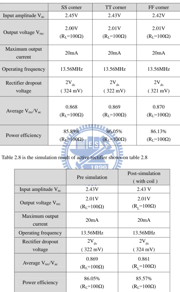
The active rectifier and high PSR low drop-out regulator simulation is using TSMC 0.18um 1P6M CMOS technology. The device parameter of active rectifier (Fig. 2.29) and power mos (Fig. 2.12) is shown in table 2.1. The vbias is a voltage from current mirror circuit such that Is1 = 30uA, Is2 = 35uA and Is3 = 1uA. In addition, the device parameter of startup circuit (Fig. 2.30) and level converter circuit (Fig. 2.31) is show in table 2.2 and table 2.3 respectively. The simulation waveform of active rectifier is show in figure 2.32. The current bias Is2 (Is3) of the comparator cmp1 has to charge the parasitic capacitors Cgs of M1 (M2) when the comparator is in output high. Therefore, the actually drain current of M0 (M3) is not equal to Is2 (Is3) until the charging current of the parasitic capacitors is settled. The unsettled voltage offset Vos+ (Vos-) of M0 is easily influenced by corner variation and devices mismatch. The corner variation and devices mismatch in IC fabrication process would also cause the variation of power NMOS turn-on delay and turn-off delay. If the power NMOS
turn-on and turn-off timing is designed at Vac = Vrec exactly, the corner variation and devices mismatch may cause power NMOS turn on too early or turn off too late. The wrong operation of the power NMOS would cause the reverse leakage current and reduce the power conversion efficiency. Therefore, the power NMOS turn-on and turn-off timing should be designed at Vac > Vrec slightly to avoid corner variation and devices mismatch. Since the bond wire have parasitic inductance, the instantaneous charging current flow through bond wire would cause a voltage drop across inductance, that make Vrec node noise as show in figure 2.33. In according to section 2.1, the coil‟s inductance value, resonance capacitor value and coupling coefficient can be established into spice model as show in table 2.4. Since switching mode active rectifier is nonlinear effect to the receive coil, the voltage transient can be obtained by hspice simulation on figure 2.28. The hspice simulation shows that coil inductance cannot exceed 250nH because the high inductance value of receive coil will cause Vin voltage drop too fast. The Vin voltage fast drop will cause comparator turn off too early hence comparator will turn on and turn off again in the same cycle. The additional switching of power mos degrades the conversion efficiency.
The device parameter of voltage reference is show in table 2.5. The simulation result of PSR of voltage reference circuit is show in figure 2.34 and the voltage reference circuit power consumption is 2.7uW. The monte carol analysis of voltage reference shows that process variation may induce ±26.7 mV output voltage variation (Fig. 2.35). The PSR of voltage reference can be improved 40 dB by adding pre-regulator in front of voltage reference power supply (Fig. 2.36). The device parameter of pre-regulator is show in table 2.6. Further, the low pass filter is added on the voltage reference output to eliminate the high frequency above 1 kHz power supply noise (Fig. 2.37). The device parameter of LDO core is show in table 2.7. The LDO core stability of different corner post simulation shows on figure 2.38, that have
phase margin 80 degree at least. Figure 2.39 is temperature variation of the voltage reference output voltage. The process corner variation on PSR of whole regulator including LDO core also shows on figure 2.40. The SS corner of LDO dropout voltage must be higher than other corner. Since the power mos of the LDO have worse current conductivity. The full load transient load regulation from 0 to 20mA will cause 5.5 mV maximum undershoots and overshoots as in figure 2.41. The monte carol analysis of voltage reference and regulator shows that process variation may induce 1.81V±4.3% output voltage variation (Fig. 2.42). The final whole chip start-up mechanism shows in Figure 2.43 that LDO output voltage can gradually saturation to 1.8V under 20mA loading current. Figure 2.44 is the transient voltage on the transistor M1 of the comparator. The maximum reverse bias 2.16v occur between source and body terminal of M1. Since N+ / PW break down voltage is 11.1v, the parasitic diode between source and body terminal of M1 would not break down.
The final simulation result of active rectifier shows on table 2.8. The different process corner variation shows on table 2.9. The final simulation result of LDO regulator shows on table 2.10. The different process corner variation shows on table 2.11.
MOSFET 1.8V dimension (um / um) M0 1/5 M16 2/5 m=4 M1 1/5 m=30 M17 10/0.2 M2 1/5 m=16 M18 10/0.2 M3 1/5 M19 18/1 M4 2/1 m=4 M20 2/1 M5 2/1 m=7 M29 20/0.18 M11 18/1 M30 20/0.18 m=2 M15 2/5 m=14 Power MOSFET 3.3V Mp1 10/0.3 m=540 Mn1 20/0.35 m=75 Mp2 10/0.3 m=540 Mn2 20/0.35 m=75 Capacitor value (MIM)
C0 0.5pF C1 0.5pF Table 2.1 is the active rectifier device parameter.
MOSFET 1.8V dimension (um / um) M0 1/1 M11 12/1 M8 2/1 M13 4/1 MOSFET 1.8V medium Vt (um / um) M12 4/1
MOSFET 3.3V dimension (um / um) M0 5/0.3 M1 5/0.3 MOSFET 3.3V medium Vt (um / um)
M2 10/0.6 M3 10/0.6 Table 2.3 is the device parameter of level converter circuit.
Transmission coil L1 7 uH Cres1 18.8 pF R1 3.58 Ω Receive coil L2 223 nH Cres2 617 pF R2 0.5 Coupling coefficient k 0.101
Table 2.4 is the inductive link coil parameter.
MOSFET 1.8V dimension (um / um)
M2 0.5/20 m=10 M7 1/5 m=2 M4 0.5/20 m=2 M8 1/5 m=2 M5 2/20 m=2 M9 1/5 m=2 M6 2/20 m=2 M10 1.7/20 MOSFET 3.3V dimension (um / um)
M1 5/2.5 m=48 M3 2.5/5 m=2
MOSFET 1.8V dimension (um / um) M0 1/8 M6 8/8 M4 2/3 M24 4/4 M5 10/8
MOSFET 1.8V medium Vt (um / um) M2 2/3 M3 2/3 M1 2/8
Table 2.6 is the device parameter of pre-regulator.
MOSFET 1.8V dimension (um / um) M0 3/4 m=2 M3 4/4
M1 3/4 m=2 M4 10/1 m=3 M2 10/1 M7 4/4
Power MOSFET 1.8V Mp1 10/0.18 m=150
MOSFET 1.8V medium Vt (um / um)
M5 10/0.25 M16 2/4 m=2 M9 4/4 M17 2/4 m=2 M10 4/4
SS corner TT corner FF corner Input amplitude Vac 2.45V 2.43V 2.42V
Output voltage Vrec
2.00V (RL=100Ω) 2.01V (RL=100Ω) 2.01V (RL=100Ω) Maximum output
current 20mA 20mA 20mA
Operating frequency 13.56MHz 13.56MHz 13.56MHz Rectifier dropout voltage 2Vds ( 324 mV) 2Vds ( 322 mV) 2Vds ( 321 mV) Average Vrec/Vac 0.868 (RL=100Ω) 0.869 (RL=100Ω) 0.870 (RL=100Ω) Power efficiency 85.89% (RL=100Ω) 86.05% (RL=100Ω) 86.13% (RL=100Ω)
Table 2.8 is the simulation result of active rectifier shows on table 2.8
Pre simulation Post-simulation ( with coil ) Input amplitude Vac 2.43V 2.43 V
Output voltage Vrec
2.01V (RL=100Ω)
2.01V (RL=100Ω) Maximum output
current 20mA 20mA
Operating frequency 13.56MHz 13.56MHz Rectifier dropout voltage 2Vds ( 322 mV) 2Vds ( 324 mV) Average Vrec/Vac 0.869 (RL=100Ω) 0.861 (RL=100Ω) Power efficiency 86.05% (RL=100Ω) 85.57% (RL=100Ω)
Pre-simulation (two capacitors)
Post-simulation (two capacitors) Input voltage Vrec >2(v) >2(v)
Output voltage Vout 1.8(v) 1.8(v)
Dropout voltage >0.2(v) >0.2(v) Maximum output
current 20(mA) 20(mA) Quiescent current 97(uA) 97(uA)
Power supply rejection -60.1 (dB)@ 100kHz -55.8 (dB)@ 1MHz -69.4 (dB)@ 10MHz -60.2 (dB)@ 100kHz -55.9 (dB)@ 1MHz -69.2 (dB)@ 10MHz Transient load regulation 5.5mv@0 ~ 20mA (10ns) 5.5mv@ 0 ~ 25mA (10ns) Table 2.10 is the final simulation result of LDO regulator.
SS corner TT corner FF corner Input voltage Vrec >2.07(v) >2(v) >2(v)
Output voltage Vout
1.8(v) 1.8(v) 1.8(v) Dropout voltage >0.27(v) >0.2(v) >0.2(v) Maximum output
current 20(mA) 20(mA) 20(mA) Quiescent current 94(uA) 97(uA) 99(uA)
Power supply rejection -56.3 (dB)@ 100kHz -55.1 (dB)@ 1MHz -71.2 (dB)@ 10MHz -59.3 (dB)@ 100kHz -56.6 (dB)@ 1MHz -71.1 (dB)@ 10MHz -60.2 (dB)@ 100kHz -55.9 (dB)@ 1MHz -69.6 (dB)@ 10MHz Transient load regulation 5.7mv@ 0 ~ 20mA (10ns) 5.5mv@ 0 ~ 20mA (10ns) 5.5mv@ 0 ~ 20mA (10ns) Table 2.11 is the different process corner variation of LDO regulator.
![Figure 2.4 is the spiral coils pair for inductive link. The left coil is the transmitter part (primary part) and the right coil is the receiver part (secondary part) [16]](https://thumb-ap.123doks.com/thumbv2/9libinfo/8467900.183419/49.892.153.748.505.1042/figure-spiral-coils-inductive-transmitter-primary-receiver-secondary.webp)


![Figure 2.24 shows the various paths that could couple input ripples to the output of the LDO [19]](https://thumb-ap.123doks.com/thumbv2/9libinfo/8467900.183419/60.892.154.725.510.1005/figure-shows-various-paths-couple-input-ripples-output.webp)