國
立
交
通
大
學
電控工程
電控工程
電控工程
電控工程研究所
研究所
研究所
研究所
碩
碩
碩
碩
士
士
士
士
論
論
論
論
文
文
文
文
模組化在單迴路積分三角類比數位轉換
器中積分器充放電雜訊與諧波失真模型
Modeling Settling Noises and Distortions for
Single-Loop Sigma-Delta Modulators
研 究 生:謝武璋
指導教授:陳福川 教授
中
中
中
中
華
華
華
華
民
民
民
民
國
國
國
國
九
九
九
九
十
十
十
十
八
八
八
八
年
年
年
年
九
九
九
九
月
月
月
月
模組化在單迴路積分三角類比數位轉換器中積分器
充放電雜訊與諧波失真模型
Modeling Settling Noises and Distortions for
Single-Loop Sigma-Delta Modulators
研 究 生:謝武璋 Student:Wu-Chang Hsieh
指導教授:陳福川 Advisor:Fu-Chuang Chen
國 立 交 通 大 學
電 控 工 程 研 究 所
碩 士 論 文
A ThesisSubmitted to Department of Electrical and Control Engineering College of Electrical Engineering
National Chiao Tung University in partial Fulfillment of the Requirements
for the Degree of Master
In
Electrical and Control Engineering
September 2009
Hsinchu, Taiwan, Republic of China
模組化在單迴路積分三角類比數位
轉換器中積分器充放電雜訊與諧波
失真模型
研究生:謝武璋 指導教授:陳福川 教授 國立交通大學 電控工程研究所摘要
交換式電容積分器已經被廣泛的應用在積分三角轉換器的領域中,且由於積 分器中電容不完全的充放電轉換特性(積分器充放電問題),使得此積分器充放電 問題與其效能有著高度的相關性。因此,在現今已發表出之積分三角轉換器中,積 分器充放電問題是一個很艱難且棘手的設計課題。而因為積分器充放電問題的高 複雜性,相關的誤差和失真的解析模型實際上是不存在的。此篇論文的目地在於 利用了非線性擬合方法和輸出端頻譜預測技術來探討單迴路積分三角轉換器的 積分器充放電問題。經由上面的分析,我們可以獲得積分器充放電問題誤差和失 真的封閉解,且此封閉解可以經由積分三角轉換器中的系統參數所組成的函式呈 獻出來。我們同時利用了行為層的模擬以及電晶體層次的電路模擬來驗證此解析 模型的正確與精確性。由上面的驗證結果顯示出此兩種模擬結果與我們的解析模 型有著相當合適的一致性。Student:Wu-Chang Hsieh Advisor:Dr. Fu-Chuang Chen
Institute of Electrical and Control Engineering Nation Chiao Tung University
ABSTRACT
Switch-capacitor (SC) integrators have been widely used in sigma-delta modulators (Σ∆Ms) and the performances of SC integrators depend highly on their incomplete charge-transfer (settling problem) behavior. Therefore, the settling problem is a crucial design concern in well-published switch-capacitor Σ∆Ms. Due to the complexity of settling problem, analytic models for related noises and distortions are virtually non-existent. The aim of this paper attempts to explore the settling problems on single-loop Σ∆Ms by employing nonlinear fitting methods and output spectrum prediction techniques. Closed forms of settling error and settling distortion models are acquired, and are represented as functions of Σ∆ modulator system parameters. Both behavior simulations and transistor-level-circuit simulations are employed to verify these analytical models. The results of above validation showed an appropriate level of consistence between the two simulations and our analytical models.
Modeling Settling Noises and Distortions for
Single-Loop Sigma-Delta Modulators
Acknowledgment
此篇論文的完成首先要感謝陳福川教授在我兩年的碩士班過程中指導我在研究 以及學術上的想法,讓我能夠獲得老師在學術上的經驗以自我成長。其次要感謝 畢業的黃俊傑學長在我有所疑問時的輔助以及幫忙,讓我能達到事半功倍的研究 效果。同時要感謝畢業的王文佑以及沈柏年學長在同實驗室相處期間的一切幫助, 還有 608 lab 的同學謝智隆、黃瑞祺以及學弟歐嘉昌、盛子恩和我在研究上的互 相交流、討論。 感謝我的父母、雅如姐姐和其餘長輩們在我求學期間的一切支持與鼓勵、怡人 姐姐以及順欽姐夫在生活上的照顧。也謝謝子誠、瑋琳、柏元、柏勛、立杰這群 朋友帶給我在學校生活之外的成長與歡樂。最後感謝我最愛的女朋友,遠在 Loughborough University 的怡今(princess of smile)一路給我心靈上以及情 感上的陪伴,讓我能順利渡過這兩年碩士生活。Contents
中文摘要 ... I
English Abstract...II Acknowledgment...III Contents ...IV Lists of Tables ...VI Lists of Figures ...VII List of Symbols ...X
Chapter1 Introduction...1
1.1 Current Status and Background...1
1.2 Motivation and Aims...3
1.3 Organization...5
Chapter2 Architecture of
Σ∆
Modulators...62.1 First-Order Sigma-Delta Modulator...6
2.2 Single-Loop Second-Order Sigma-Delta Modulator...8
2.3 Single-Loop High Order Sigma-Delta Modulator...10
2.4 Quantizer Nonlinearity Of Sigma-Delta Modulator...11
2.5 Performance for a Σ∆ Modulator...12
Chapter3 Investigation of
Σ∆
Modulators Settling Problems...143.1 Settling Noise of Sampling Phase and Integration phase...15
3.2 Properties of V ... ………...18 S Chapter4 Derivation of Sigma-Delta Modulator Settling Noise Power Model….…..23
4.1 Settling Errors of Sampling Phase...24
4.2 Settling Errors of Integration Phase...25
Chapter6 Simulation Results and Validation………..54 Chapter7 Conclusions and Discussions……….…58
Lists of Tables
Table 3.1 Standard deviations of VS (2nd-order) vs. different quantizer bit numbers
………..19 Table 3.2 Standard deviations of VS (1st-order) vs. different quantizer bit numbers
………..21 Table 3.3 Standard deviations of VS (3rd-order) vs. different quantizer bit numbers
………..22 Table.4.1 Coefficients obtained in three different cases
………..29 Table.4.2 The effect of SR on settling noise……….37
Table.4.3 Minimum SR and GBW required w. r. t. OSR
………....43 Table.5.1 Minimum SR and GBW required w. r. t. OSR
………53 Table.6.1Simulation parameters in Fig. 6.3
Lists of Figures
Fig. 2.1 First-order Σ∆ modulator...6
Fig. 2.2 Single loop second order Σ∆ modulator...8
Fig. 2.3 Comparison of noise shaping techniques...9
Fig. 2.4 Single-loop high order Σ∆ modulator...10
Fig. 2.5 Performance characteristic of a Σ∆ converter...13
Fig. 3.1 Single loop second order Σ∆ modulator...14
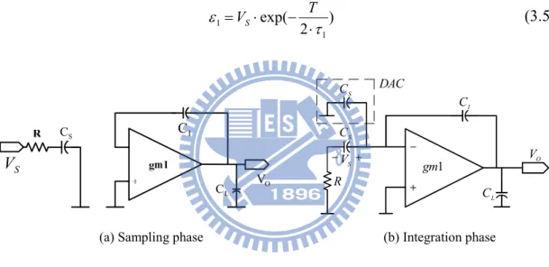
Fig. 3.2 A typical SC integrator with DAC branches...15
Fig. 3.3 Switched capacitor integrator diagrams...16
Fig. 3.4 Simulated results of VS distribution...18
Fig. 3.5 PSD of VS... ...19
Fig. 3.6 Simulated results of VS with AVS = 0.5, OSR = 16, and different Bits………20
Fig. 4.1 Settling noise of integration phase under different SR and GBW values (a)SR=100 V/us, GBW=100 MHz (b)SR=30 V/us, GBW=55 MHz...24
Fig. 4.2 Nonlinear transfer function of (4.3) ...25
Fig. 4.3 Distribution of VS obtained in three different cases (a) Behavioral model (b) With Gaussian distribution (c) No Gaussian distribution...29
Fig. 4.4 Settling error versus VS in three different cases...30
Fig. 4.5 The distribution of angle of VS……...30
Fig. 4.6 Height of PSD of square of VS (a) Included f = 0 (b) Not included f = 0...31
Fig. 4.7 Integration of the convolution (a) A result of convolution
(b) Sum of overlap part of (a)...32
Fig. 4.8 Comparison of the expected value of (4.17) with the behavior simulation result... 33 Fig. 4.9 Comparison of the expected value of VS 3 with the behavior simulation
result ... 34 Fig. 4.10 Comparison of the expected value of VS 5 with the behavior simulation
result ... 35 Fig. 4.11 Settling noise of integration phase under different SR and GBW values
(a) SR=100 V/us, GBW=100 MHz
(b) SR=30 V/us, GBW=55 MHz...36 Fig. 4.12 Settling noise of integration phase under different SR and GBW values (first-order)
(a) SR=200 V/us, GBW=200 MHz
(b) SR=60 V/us, GBW=70 MHz...40 Fig. 4.13 Settling noise of integration phase under different SR and GBW values (third-order)
(a) SR=200 V/us, GBW=200 MHz
(b) SR=60 V/us, GBW=70 MHz...41 Fig. 4.14 Comparison of settling noise of first, second and third order Σ∆ modulators
(a) SR=200 V/us, GBW=200 MHz
(b) SR=60 V/us, GBW=70 MHz...42
Fig. 5.1 Nonlinear transfer function of (5.6) ...45 Fig. 5.2 Output spectrum of a second-order Σ∆ modulator with settling harmonic
Fig. 5.3 SR versus HD3...52
Fig. 5.4 GBW versus HD3...52
Fig. 6.1 Circuit-level schematic of spice simulation………54
Fig. 6.2 Quantizer of spice simulation……….55
Fig. 6.3 Comparison of our theoretical result with transistor-level and behavior simulation result………...…56
List of Symbols
Symbols
VLSB Quantizer step size
OS
V Maximum output swing of op-amp OSR OverSampling Ratio
n Order of the Sigma-Delta modulator
B Number of bits in the quantizer
S
f
Sampling FrequencyB
f Signal Bandwidth
ref
V
Reference Voltage of the quantizer0
A Finite Gain of OTA
in
f Frequency of the input signal
i
φ
ith phase of a nonoverlap clockin
A
Amplitude of input signal.
jit
σ standard deviation of clock jitter
S
C
Sampling capacitorI
C
Integrating capacitorL
C
Load capacitor of OTALogic
C
The loading capacitors of CMOS logic gatesgate
C
The gate capacitances of all CMOS transmission gatesOX
C The capacitance per unit area of the gate oxide
S
V
Input signal plus feedback DAC signal1
τ
Time constant of input branchVS
σ Standard deviation of
V
S2
τ
Time constant of integrator output settlingη percentage of the bottom plate parasitic
T Absolute temperature
R Switch ON resistance N quantizer levels
gm1 Amplifier transconductance Pr() Probability of some condition
.
cap
σ Mismatch of unit capacitance
k Boltzmann’s constant (1.38×10⁻²³) J/K
α
OTA noise factor []Erf Error Function
OTA
I
Total current of the OTAB
I
Bias current of each transistor of the input differential pair of OTAOTA
k The ratio of the total current of the OTA to this bias current
2
cl
f The GBW of the OTA reff
V The overdrive voltage of the transistor of the input differential pair of OTA
Cs
k The ratio between the summation capacitance of
C
S in all stages and the one in the first stage0
ε
The permittivity of free space S1.Introduction
1.1 Current Status and Background
Sigma-delta modulators( Σ∆ Ms) are widely employed in many modern applications such as telecommunications, multimedia, sensors-interface and precision measurement systems, especially used for implementation of analog-to-digital converters(ADCs) with high-resolution and low-power [1-10]. Compared to the traditional converters, Σ∆modulators have achieved the most attraction recently in data converter systems due to their noise shaping and oversampling behavior that lead them to superior linearity and accuracy, simple realization, low sensitivity to circuit imperfection [11], and are more suitable for the implementation of A/D interfaces in modern standard CMOS technologies [12].
Σ∆ modulators can be implemented either with continuous-time(CT) or switched-capacitor (SC) approach. The most popular approach is based on a sampled-data solution with SC integrators implementation. Its incomplete charge transfer and the characteristics of the operational amplifiers decline drastically the performance of Σ∆ modulators. As the clock frequency increases in Σ∆ modulators to cope with wideband applications, SC integrators defective settling problem become the bottle neck in present designs. Due to the complexity of settling problem, analytic models for related noises and distortions are virtually non-existent. Transient charge transfer in SC integrators and proposed several time-domain-based behavioral descriptions have been studied by former authors[13-16], which can be used in behavior simulations. Behavioral simulations are time-consuming, unobvious, and difficult to observe settling affection in entire modulators from other nonlinearities. In addition, analytical efforts have been actually seen before. In [17-19], a thorough transient analysis for the charge-transfer error was carried out by assuming linear
feedback inherent in the Σ∆ modulators. In [20-21], the distortion due to operational transconductance amplifier (OTA) dynamics has been analyzed and modeled. It uses power expansion and nonlinear fitting to obtain analytical model to represent harmonic distortion of single bit modulator as a function of the slew-rate (SR), gain-bandwidth (GBW), and nonlinear DC gain. Unfortunately, the author provides little or no insight on how oversampling-ratio (OSR) can be influenced the system performance, and the settling noise model was not discussed. It is coarsely assumed in [22] that the settling noise is white noise contribution and the associated power spectral density (PSD) is constant in the sampling interval, but this assumption is divergent in comparison to the realistic phenomenon.
1.2 Motivation and Aims
Σ∆ modulators are extremely nonlinear sampled-data circuits, and hence, the designing of Σ∆ modulators would be a predictably tough task. As several studies have suggested the one of the best way of designing Σ∆ modulators is achieved by using the so-called behavioral simulation technique [23-24]. In this approach the modulator is separated into a set of sub-blocks. These blocks are described by equations that express their outputs in terms of their inputs and their internal related parameters. Thus, the accuracy of simulation depends on how closely those equations describe the actual behavior of each building block. From the technique discussed above, the Σ∆modulator implementation based on numerical optimization [21,25-26] is previously reported, which are based on an iterative optimization process in which the synthesis problem is formulated as a cost function, and requires many computation until best performance is achieved. If the best performance achieved still cannot meet the design specification, this strategy can provide helpful clue about the dominating nonlinearity. In contrast, design and optimization based on analytical noise and distortion models can be a more efficient and dependable approach [27, 28], as long as all of the important noise and distortion models are available. There have been a number of literatures that many noise and distortion models have derived for
Σ∆ modulators, but analytical model for switched-capacitor(SC) integrators settling noise model is never seen in the literatures, and it seems premature to discuss the settling distortion model without specifying the effect of quantizer bit number. For these reasons, the major goal of this paper is to provide the settling noise model and to supplement the finding of the earlier settling distortion model.
The settling problems of the SC integrators are mainly caused by non-idealities of OTA such as finite dc gain, finite GBW, and SR limitations. Our following works
cause the nonlinear transfer characteristics, which not only cause signal distortions, but also reflect high-frequency noises into base band. In light of these concerns, the purpose of our study is to obtain closed-form of settling error and settling distortion analytical models by using nonlinear fitting methods and output spectrum prediction techniques. These analytical models are represented as functions of Σ∆ modulator system parameters. Both behavior simulations and HSPICE circuits are employed to verify these analytical models, and the results show that our analytical models are sufficiently accurate.
1.3 Organization
This paper is organized as follows. In Chapter 2, the basic architectures and knowledge of Σ∆ modulators are introduced. In Chapter 3, the motivation of
Σ∆modulators settling problem and characteristics of the SC integrator input end are discussed. In Chapter 4, the formulation of analytical settling noise power model for first, second and high order Σ∆modulators are presented with several analytical discussions. In Chapter 5, we derive the settling distortion model, and discuss the effects between the system parameters with settling distortion. In Chapter 6, the behavior simulations and HSPICE-circuit simulations are used to validate our model. Moreover, we propose several analytical discussions. Finally, we summarize some conclusions and discussions in Chapter 7.
2.
Architectures of
Σ∆
Modulators
This section we introduce basic architectures of Σ∆ modulators. In our paper, we will focus on the single-loop module for Σ∆ modulators. First, second, and high order single-loop Σ∆ modulators will be discussed. In order to understand the system performance merits used to specify the behavior of Σ∆ modulators, several specifications concerning the performance have been discussed [28], and we incorporate it finally.
2.1 First-Order Sigma-Delta Modulator
Fig. 2.1. shows a standard architecture of first order sigma-delta modulator. Here, H(z) is 1 1 Z 1 Z − −
− ; Analyze transfer function H(z) from time-domain, it indicates that
output signal m(t) is obtained by adding the delayed input signal n(t-1) and the delayed output signal m(t-1), so we can express a complete first-order Σ∆ modulator as Fig. 2.1. Z-1 x(n) H(z) y(n) D/A Quantizer e(n)
Fig. 2.1 First-order Σ∆ modulator
H(z) in Fig. 2.1 is indicated the effects of delay and accumulation, this is equivalent with an integrator in circuit design, so the three circuits components of Σ∆
modulator are integrator, quantizer and DAC in the feedback path. A first order Σ∆ modulator’s output can represent as
Y(z)=z-1X(z) + (1-z-1)E(z) (2.1)
From (2.1) we can find the signal transfer function is as a delay function, and noise transfer function is as a high pass filter, moves the noise to high frequency. In order to derive PSNR(Peak Signal-to-Noise Ratio) of first order Σ∆ modulator, we must get the magnitude of NTF(z) and STF(z) in the frequency domain, so we substitute z with
s
f f j
e 2ππππ⋅ / , and get STF(f) and NTF(f) respectively as:
1 j2πf/fs TF(f) z e S = − = − ⋅ =1 (2.2) NTF(f) = 1-e−j2π⋅f/fs= j f/fs s e j 2 ) f f sin(π × × −π⋅ ⇒ ( ) 2 sin( ) s TF f f f N = ⋅ π (2.3) So the quantization noise in base band ±fB can obtain (2.3)
PQ = df f f sin 2 f 12 V df ) f ( N ) f ( S 2 f f s s 2 LSB 2 TF f f 2 e B B B B ⋅ ⋅ ⋅ = ⋅
∫
∫
− − π (2.4)Because that fB is much lower than fs, so sin(
π
f/fs) is approximate equal to (π
f/fs),and PQ is as PQ = 3 2 2 LSB ) OSR 1 ( 36 V ⋅ π = 2B 3 2 2 OSR 2 36 FS ⋅ ⋅ ⋅π (2.5)
Assume that input signal is sinusoidal, expressed as Vin(t) = A sinωt, so the input
signal power Vin(rms)2 is as(2.6). In (2.6), we define the amplitude of input signal is
the full scale of reference voltage Vin(rms)2 =
∫
− ⋅ ⋅ 2 / T 2 / T 2 dt ) t sin A ( T 1 ω = 2 A2 = 8 ) A 2 ( 2 = 8 FS2 (2.6)PSNR = 10 log( Q signal P P ) = 10 log( 22B 2 3 ) + 10 log[ 32 (OSR)3 π ] = 6.02B + 1.76-5.17 + 30 log(OSR) (2.7)
From (2.7), we find that each octave of OSR, PSNR will increase 9dB, increase 1.5 bit in resolution. Compare (2.7) with A/D converter only has oversampling effect; we can find that 1st order noise shaping increases the performance of Σ∆ modulator.
2.2 Single-Loop Second-Order Sigma-Delta Modulator
When the discrete time filter H(z) in Fig. 2.1 is replaced by two cascade integrator, then it is a second order Σ∆ modulator, output of the first integrator is only connecting with the input of the second integrator, it is shown in Fig. 2.2
Fig. 2.2 Single loop second order Σ∆ modulator
Then the output of it can easily be derived as
Y(z) = z-2X(z) + (1-z-1)2E(z) (2.8)
where STF and NTF is as
STF(z) = z-2 (2.9)
NTF(z) = (1- z-1)2 (2.10)
Using the same method in (2.3) (2.4), we can obtain
2 s TF f f sin 2 ) f ( N ⋅ = π (2.12) PQ = 5 4 2 LSB OSR 60 V ⋅ ⋅π = 2B 5 4 2 OSR 60 2 FS ⋅ ⋅ ⋅π (2.13)
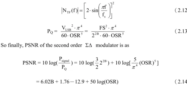
So finally, PSNR of the second order Σ∆ modulator is as
PSNR = 10 log( Q signal P P ) = 10 log( 22B 2 3 ) + 10 log[ 54 (OSR)5 π ] = 6.02B + 1.76-12.9 + 50 log(OSR) (2.14)
In the single loop second order architecture, each octave of OSR can increase PSNR by 15 dB, it is equivalent to 2.5 bit in resolution. If we compare (2.12), (2.3) with
) f (
NTF =1 that without noise shaping, as Fig. 2.3, we can find that in our needed
signal bandwidth, the quantization noise is highest when NTF(f)=1, and that with second order noise shaping is smallest among this figure.
TF
N
2 fS
2.3 Single-Loop High Order Sigma-Delta Modulator
The simplest way to extend a Σ∆ modulator towards an arbitrary Lth-order filtering consists of including L integrators before the quantizer. Extending the second order Σ∆ modulator in Fig. 2.2, the architecture in Fig. 2.4 can be obtained, which is a single loop high order Σ∆ modulator, its output would yield
Y(z) = z-LX(z) + (1-z-1)LE(z) (2.15)
Here L is order, from the derivation in Section 2.1 and Section 2.2 we can get the quantization noise PQ in signal bandwidth is as
PQ = 2L 1 L 2 2 LSB ) OSR 1 ( 1 L 2 12 V ⋅ + + ⋅ π (2.16) and its PSNR is PSNR=6.02B+1.76-10 log( 1 L 2 L 2 + π )+(20L+10) log(OSR) (2.17)
In the application of high order Σ∆ modulator, (6L+3) dB increases in SNR when OSR is octave, so PSNR can be raised by increasing the order of the system, especially at large oversampling ratio. But sometimes in high order architecture, the performance will be worse than result predicted by (2.14), because of the stability problem, it will make less effective noise shaping function, so the quantization noise will not be suppressed completely.
2.4 Quantizer Nonlinearity Of Sigma-Delta Modulator
In this section, we supplement some notion about the quantizer. The quantization operation is inherently nonlinear because the quantizer error is determined from the quantizer input signal. For convenience, we usually model the quantizer as a linear model and approximate the quantization noise as a white noise. This approximation is made when the quantization error has the following properties, which we refer to collectively as the “input-independent additive white noise approximation” [11]:
Property 1. εn is statistically independent of the input signal or
ε
n is uncorrelated with the input signal.Property 2.
ε
n is uniformly distributed in [−∆ 2,∆ 2].Property 3.
ε
n is an independent identically distributed (i.i.d.) sequence orε
n has a flat power spectral density.where
ε
n is the error sequence and ∆ is the distance between output levels. Therefore, the quantization error from Σ∆ modulators is typically not white. For dc inputs, the quantization noise spectrum consists of discrete spectral lines, called idle channel tones or pattern noise. For ac inputs, the quantization noise spectrum comprises all harmonics of system input frequency and amplitude as one might expect with a nonlinear device [29]. One can view this effect as a time-domain distortion and therefore argue that the converter actually has less resolution than rms measurements. In fact, the decorrelation between the quantization errorε
n and the input signal increases with the modulator order. This, together with circuit noise acting as a dithering signal in practical implementations, greatly helps to palliate the coloration ofuse it in the latter chapter.
2.5 Performance for a
Σ∆Modulator
We collect several performance indices which often used to specify the behavior of Σ∆ modulator.
․Signal to Noise Ratio: The SNR of a data converter is the ratio of the signal power to the noise power, measured at the output of the converter for a certain input amplitude. The maximum SNR that a converter can achieve is called the peak SNR.
․Signal to Noise and Distortion Ratio: The SNDR of a converter is the ratio of the signal power to the power of the noise and the distortion components, measured at the output of the converter for a certain input amplitude. The maximum SNDR that a converter can achieve is called the peak SNDR.
․Dynamic Range at the input: The DRi is the ratio between the power of the largest input signal that can be applied without significantly degrading the performance of the converter, and the power of the smallest detectable input signal. The level of significantly degrading the performance is defined as the point where the SNDR is 6 dB bellow the peak SNDR. The smallest detectable input signal is determined by the noise floor of the converter.
․Dynamic Range at the output: The dynamic range can also be considered at the output of the converter. The ratio between maximum and minimum output power is the dynamic range at the output DRo, which is exactly equal to peak SNR.
․Effective Number of Bits: ENOB gives an indication of how many bits would be required in an ideal quantizer to get the same performance as the converter. This numbers also includes the distortion components and can be calculated as:
02 . 6 76 . 1 ENOB= SNR− (2.18)
․Overload Level: OL is defined as the relative input amplitude where the SNDR is decreased by 6dB compared to peak SNDR
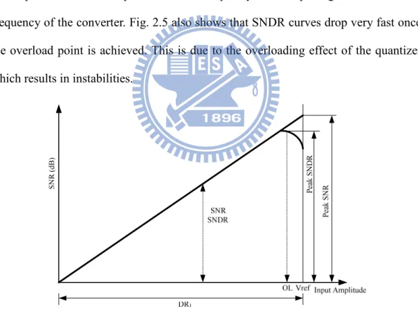
Typically, these specifications are reported using plots like Fig. 2.5. This figure shows the SNR and SNDR of the Σ∆ converter versus the amplitude of the sinusoidal wave applied to the input of the converter. For small input levels, the distortion components are submerged in the noise floor of the converter. Consequently, the SNDR and SNR curves coincide for small input levels. When the input level increases, the distortion components start to degrade the modulator performance. Therefore, the SNDR will be smaller than the SNR for large input signals. Note that these specifications are dependent on the frequency of the input signal and the clock frequency of the converter. Fig. 2.5 also shows that SNDR curves drop very fast once the overload point is achieved. This is due to the overloading effect of the quantizer which results in instabilities.
3.
Investigation of
Σ
−
∆
Modulators
Settling Problems
In practice, dynamic limitations in switched-capacitor integrators, basically due to the finite GBW and SR of the amplifiers, induce non-linear behavior in the charge transfer. The impact of the associated output settling problem on the modulator performance will be higher, the higher the sampling frequency. In order to understand why there is such serious, it is necessary to examine the evolution of the notion of settling problem. Previous papers have mentioned the settling problem [15,30]. Therefore, in this section, we firstly clearly define the settling error in switched-capacitor integrators. Due to the input of SC integrator, called VS,
dramatically affect the SC integrator performance, so we examine the properties of VS
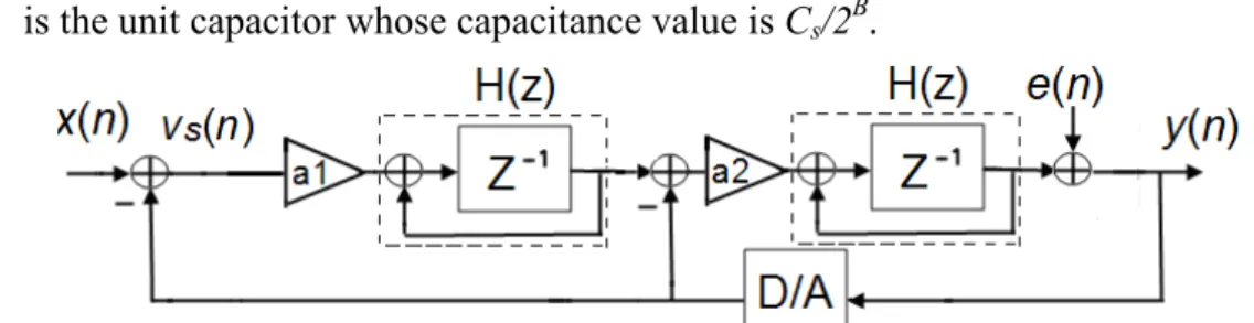
later. We focus on second order module, and the procedure of first, high order module will be similar. Since the settling problem at later stages are less influential due to noise shaping, so we only consider the settling problem of first stage integrator. Fig. 3.1 indicates a standard architecture of second order sigma-delta modulators. As stated before, where H(Z) = 1
1 Z 1 Z − −
− is the transfer function of switched-capacitor integrator, a1=0.5 and a2=2 are used for stability of entire modulator. The Fig. 3.2 shows a typical scheme of switched capacitors integrators with DAC branches. Here,
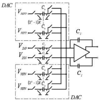
Cμ is the unit capacitor whose capacitance value is Cs/2B.
Fig. 3.2. A typical SC integrator with DAC branches
3.1 Settling Noise of Sampling Phase and Integration Phase
Sampling and integration phase will be analyzed separately. Fig. 3.3 illustrates sampling and integration phase of SC integrators with the MOS switched on-resistance R and the transconductance of OTA, gm1. Let the output parasitic capacitor be CL ≅η⋅CI , where η is the percentage of bottom plate parasitic,
assumed to be 20%[31]. In Fig. 3.3(a), the voltage VS represents the difference
between the sinusoid input signal and the feedback signal from DAC:
)
(
)
(
)
(
z
X
z
Y
z
V
S=
−
(3.1)As stated before, in a second-order Σ∆ modulator, modulator output signal Y(z) is the time delay version of X(z) plus high-pass filtered (noise shaped) quantization noise (1-z-1)2E(z). Therefore,
)
(
)
1
(
)
(
)
(
z
z
2X
z
z
1 2E
z
Y
=
−+
−
− (3.2)[
1
]
(
1
)
(
)
)
(
)
(
z
X
z
z
2z
1 2E
z
V
S=
−
−−
−
− (3.3)It is sampled by Cs, so Cs is charged in the half clock period T/2 to the voltage
VCS: )] 2 exp( 1 [ 1
τ
⋅ − − ⋅ =V T VCS S (3.4)where τ1=Rs⋅Cs is the time constant of the sampling phase in the input branch. So
the setting error during the sampling phase is:
) 2 exp( 1 1 τ ε ⋅ − ⋅ =VS T (3.5) S C S V I C L C VO S V 1 gm I C L C S C R O V S C DAC
(a) Sampling phase (b) Integration phase Fig. 3.3 Switched capacitor integrator diagrams
Next, we consider the integration phase shown in Fig. 3.3(b), where the 2B unit capacitors are combined intoCs, and the 2B DAC switches are neglected. The charge
stored in sampling capacitor will be added to the integration capacitor and this charge current is supplied by OTA. So when the slew rate and gain bandwidth are not large enough, the settling error
ε
2 will become nonlinear. According to absolute value of VS, three types of settling conditions will happen in the integrator output duringintegration phase, and the corresponding voltage errors
ε
2 of these three conditions are [15]:1. Linear settling: When the initial change rate of the integrator output voltage (Vo) is
smaller than the OTA slew rate (SR).
) 2 exp( 2 1 2 ττττ εεεε ⋅ − ⋅ ⋅ =a VS T , when 2 1 1 0< < ⋅SR⋅τ a VS (3.6)
2. Partial slewing: The initial change rate of Vo is larger than SR, but it gradually
decreases until it is below the slew rate.
1) 2 exp( ) sgn( 2 2 1 2 2 − − ⋅ ⋅ ⋅ ⋅ ⋅ = ττττ ττττ ττττ εεεε T SR V a V SR S S , when 1 2 2 1 ) 2 ( 1 a SR T V SR a ⋅ ⋅τ < S < +τ (3.7)
3. Fully slewing: The initial change rate of Vo is larger than SR, and it maintains
above SR in the 2 T interval. 2 ) sgn( 1 2 T V SR V a ⋅ S − ⋅ S ⋅ = εεεε when ) 2 ( 2 1 τ + > T a SR VS (3.8)
where SR is the slew rate of OTA, and
GBW Cs R GBW ⋅ ⋅ ⋅ ⋅ + = π π τ 2 2 1 2 [30] is the time
constant in the integration phase, with GBW being the equivalent gain bandwidth in the integration phase. The capacitor loading in OTA output during this phase is heavier than in the sampling phase, and is [28]
I S I L S L C C C C C C 2 2 (2 ) + ⋅ + = (3.9) The GBW is given by π 2 2⋅ = L C gm1 GBW (3.10)
3.2 Properties of
VSIn this section, we separately discuss the time-domain and frequency-domain properties of VS to find out the time-domain probability distribution and the P.S.D of
VS. These properties will be used to do nonlinear fitting and spectrum construction of
settling noise in next chapter.
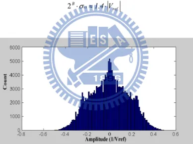
Firstly, we need to find the VS time-domain statistical property. Simulations results
(using SIMULINK) on a second-order Σ∆ modulator with a1 = 0.5, a2 = 2, 10-level
quantization, reference voltage Vref = 1, and a full scale sinusoidal input signal, are
shown in Fig. 3.4. The result is close to a Gaussian distribution. Therefore, we assume VS is Gaussian distributed with a zero mean. The standard deviations σ of VVS S under different quantizer levels are tabulated in Table 3.1. We observed that when the quantizer level N increases, σ decreases. From this table, the relation between VS standard deviation σ and quantizer levels 2VS B can be approximated by
ref vs B V 1.4 ⋅ ≈ ⋅σ 2 (3.11)
TABLE 3.1
Standard deviations of VS (2nd-order) vs. different quantizer bit numbers Std. deviation (σVS) Variance Quantizer level (N) Bit number (B) 0.711 0.506 2 1 0.455 0.207 3 1.585 0.282 0.080 5 2.322 0.206 0.042 7 2.808 0.155 0.024 9 3.17 0.136 0.018 11 3.46 0.048 0.002 31 4.95
Next, we must determine the P.S.D of VS. An expression for VS has been given in (3.3)
[
1]
(1 ) ( ) ) ( ) ( 2 1 2 z E z z z X z VS − − − − − =The PSD of VS of second order Σ∆ modulator which simulates with OSR = 16, SR =
60V/µs, GBW = 130M, and a 100kHz sinusoidal input signal is plotted in Fig. 3.5. In order to calculate the PSD of VS, we separately discuss the part of E(z) and X(z). We
firstly ignore X(z) in (3.3) and express VS as
) ( ) 1 ( ) ( 1 2 z E z z VS = − − (3.12) 103 104 105 106 -200 -180 -160 -140 -120 -100 -80 -60 -40 -20 0 frequency (Hz) P o w e r S p e c tr u m D e n s it y ( d B ) Fig. 3.5. PSD of V
Then the magnitude of E(z) must be determine. The range of quantization error is limited in ±VLSB/2, and we assume the probability density function of quantization
error is uniformly distributed between ±VLSB/2 and its mean is zero. From this
assumption, the total quantization noise power can be calculated as
12 2 2 LSB q V e = (3.13) B LSB FS V 2 = (3.14)
FS=Full scale = Vref+-Vref- B:Quantization bit number
Since all the noise power of quantization error is folded into the frequency band
2 / ~ 2 / s s f f
− and power spectral density is white, we can easily get the height of power spectral density of quantization noise.
s LSB e f V h 12 = (3.15)
Then we substitute z with ej2πf/fs in (3.12) and magnitude of V
S can be defined as s B s s f FS f f f V 12 2 sin 2 ) ( 2 ⋅ ⋅ = π (3.16)
So the relationship between the magnitude of VS and the bits number translates to a
gain. Fig. 3.6 shows that the shape of VS is not related to bits which can only affect the
level of quantization noise floor.
Then we consider the part of X(z) and ignore the E(z) in (3.3) to express VS as ) ( ) 1 ( ) (z z 2 X z VS − − = (3.17)
Take the inverse z-transform to (3.17)
) T t ( u ) T t ( x ) t ( x ) t ( VS = − −2 −2 ) 2 ( )) 2 ( sin( ) sin( t A t T u t T Ain − in − ⋅ − = ω ω (3.18)
Then, the amplitude of VS can be obtained as
T A T A T x T V AVS = S(2 )= (2 )= insin(
ω
⋅2 )≅2 in⋅ω
⋅ (3.19)Note that AVS is not related to quantizer bit number B. The result has been verified by
behavior simulation under different B values, as shown in Fig. 3.6.
The analytic procedure of first, and high order single-loop modulators will be similar to above discussion. We just show the results of it in Table 3.2. , Table 3.2. :
TABLE 3.2
Standard deviations of VS (1st-order) vs. different quantizer bit numbers Std. deviation (σVS) Variance Quantizer level (N) Bit number (B) 0.331 0.110 2 1 0.254 0.065 3 1.585 0.176 0.031 5 2.322 0.129 0.017 7 2.808 0.091 0.008 9 3.17 0.066 0.004 11 3.46 0.026 0.0006 31 4.95
TABLE 3.3
Standard deviations of VS (3rd-order) vs. different quantizer bit numbers Std. deviation (σVS) Variance Quantizer level (N) Bit number (B) 1.305 1.703 2 1 0.864 0.746 3 1.585 0.520 0.270 5 2.322 0.369 0.136 7 2.808 0.287 0.082 9 3.17 0.235 0.055 11 3.46 0.085 0.007 31 4.95
From these tables, the relation between standard deviation σ and quantizer levels VS 2B can be approximated by ref V 0.8 2B⋅σσσσvs≈ ⋅ (1st-order) (3.20) ref V 2.6 2B⋅σσσσvs≈ ⋅ (3rd-order) (3.21)
4.
Derivation of Sigma-Delta Modulator
Settling Noise Power Model
The purpose of this section is to derive the analytical Σ∆ modulator output models of settling noises and express in noise power form. This derivation is divided into sampling phase and integration phase.Most of the complexity appears in integration phase. Non-idealities in OTA can cause nonlinear transfer characteristics, which can increase the noise power within base band. These nonlinearities are approximated by a nonlinear fitting which takes into account the time-domain distribution of SC integrator input VS described in (3.11). Then circular convolution is employed to
synthesize the PSD of settling noises at Σ∆ modulator output, using the height of PSD of noise part of VS given in (3.16). Our results will quantitatively explain how
these OTA transfer nonlinearities can reflect high-frequency noises into base band, this phenomenon is demonstrated in Fig. 4.1, Fig. 4.1(a) show the output PSD of an ideal Σ∆ modulator without nonlinear settling problem. When SR and GBW of OTA are not large enough, nonlinear effects will become obvious and it can reflect high-frequency noises into base band, resulting in a large and flat noise floor in base band as is shown in Fig. 4.1(b). Due to the derivations of first and high order Σ∆
modulator will be similar as second order, we abbreviate it and discuss valuable insights of first and high order finally in comparison with second order.
104 105 106 107 -180 -160 -140 -120 -100 -80 -60 -40 -20 Frequency (Hz) P o w e r S p e c tr u m D e n s it y ( d B ) (a) SR=100 V/us, GBW=100 MHz 104 105 106 107 -100 -90 -80 -70 -60 -50 -40 -30 -20 -10 Frequency (Hz) P o w e r S p e c tr u m D e n s it y ( d B ) (b) SR=30 V/us, GBW=55 MHz
Fig. 4.1 Settling noise of integration phase under different SR and GBW values
4.1 Settling Errors of Sampling Phase
From (3.5) and (3.16), we can obtain the sampling-phase settling noise power at
Σ∆ modulator output by integrating the PSD of sampling-phase settling noise, i.e. )
(
2
1 f
∫
∫
− −
−
×
=
=
B B B B f f s s s LSB f f e TFdf
T
f
f
f
V
df
f
N
f
S
P
2 1 2 2 2 2)
2
exp(
)
(
sin
4
12
)
(
)
(
1ττττ
ππππ
εεεε (4.1)4.2 Settling Errors of Integration Phase
As was mentioned above chapter, there are three settling conditions depending on the absolute value of VS. The full slewing case is not considered here because it is not
significant. Note that VS at end of each integration interval can be written as
>
−
≤
−
=
− L S V V S L S L S S SV
V
e
e
V
V
V
a
V
V
V
a
T
V
L S)
;
1
(
;
)
1
(
)
(
1 1 1ββββ
ββββ
(4.2)where β =exp(−Ts/2τ2) and VL =SRτ2/ a1
From(4.2),the settling error of integration phase can be calculated as following expression, and we draw it in Fig. 4.2:
>
≤
=
− L S V V L S L S S SV
V
e
e
V
V
a
V
V
V
a
V
L S;
)
sgn(
;
)
(
1 1 1 2β
β
ε
(4.3)Fig. 4.2 nonlinear transfer function of (4.3)
reasons of symmetry of Fig. 4.2. Then (4.3) can be approximated by ) ( ) ( S 1 1 S 3 S3 5 S5 i V a V V V p =
α
α
α
α
+α
α
α
α
+α
α
α
α
(4.4)The pi(VS) should be fitted through all the points in 0~VH, where VH is defined as the
maximum value of VS, so that the sum of the squares of the distances of those points
from the pi(VS) is minimum. The sum of the squares is
[
]
S V S S pV dV V q=∫
H − 0 2 2( ) ( )ε
[
]
S V S S S Sa
V
a
V
a
V
dV
V
H 2 0 5 5 1 3 3 1 1 1 2(
)
∫
−
−
−
=
ε
α
α
α
(4.5)With the method above, the coefficients in (4.5) for q to be minimum can be the solution of follow equations.
[
]
[
]
[
]
= − ∂ ∂ = − ∂ ∂ = − ∂ ∂∫
∫
∫
0 ] ) ( ) ( [ 0 ] ) ( ) ( [ 0 ] ) ( ) ( [ 0 2 2 5 0 2 2 3 0 2 2 1 S V S S S V S S S V S S dV V p V dV V p V dV V p V H H H ε α ε α ε α (4.6)Note that the distribution of VS in (4.6) is assumed to be uniform over 0~VH. This may
lead to a bad estimation of settling noise, especially in the case of small VL. As
mentioned before chapter, the distribution of VS have been defined as Gaussian
distribution with standard deviation V Vref B S ≈1 ⋅.4 /2
σ σσ
σ (second-order). There, the
probability density function (PDF) of VS is
)
2
exp(
2
1
)
(
2 2 S S V S V sV
V
f
σ
σσ
σ
σ
σσ
σ
ππππ
−
=
(4.7))
2
exp(
2
1
)
2
exp(
2
1
1
)
(
2 2 0 2 2 S S H S S V S V V S V S V sV
dV
V
V
f
σ
σσ
σ
σ
σσ
σ
ππππ
σ
σσ
σ
σ
σσ
σ
ππππ
−
−
=
∫
(4.8)Then (4.8) is normalized and weighting function can be expressed as
)
2
exp(
2
1
)
2
exp(
2
1
)
(
2 2 0 2 2 S S H S S V S V V S V S V H SV
dV
V
V
V
W
σ
σσ
σ
σ
σσ
σ
ππππ
σ
σσ
σ
σ
σσ
σ
ππππ
−
−
=
∫
(4.9)Taking into account the PDF of VS in any specific interval, then (4.6) is revised as:
[
]
[
]
[
]
= ⋅ − ∂ ∂ = ⋅ − ∂ ∂ = ⋅ − ∂ ∂∫
∫
∫
0 ] ) ( ) ( ) ( [ 0 ] ) ( ) ( ) ( [ 0 ] ) ( ) ( ) ( [ 0 2 2 5 0 2 2 3 0 2 2 1 S V S S S S V S S S S V S S S dV V W V p V dV V W V p V dV V W V p V H H H εεεε α α α α εεεε α α α α εεεε α α α α (4.10)[
]
[
]
[
]
=
−
−
−
×
∂
∂
=
−
−
−
×
∂
∂
=
−
−
−
×
∂
∂
⇒
∫
∫
∫
0
)
(
)
(
0
)
(
)
(
0
)
(
)
(
0 5 5 1 3 3 1 1 1 2 5 0 5 5 1 3 3 1 1 1 2 3 0 5 5 1 3 3 1 1 1 2 1 S S V S S S S S S V S S S S S S V S S S SdV
V
W
V
a
V
a
V
a
V
dV
V
W
V
a
V
a
V
a
V
dV
V
W
V
a
V
a
V
a
V
H H Hα
α
α
α
α
α
α
α
α
α
α
α
εεεε
α
α
α
α
α
α
α
α
α
α
α
α
α
α
α
α
εεεε
α
α
α
α
α
α
α
α
α
α
α
α
α
α
α
α
εεεε
α
α
α
α
[
]
[
]
[
]
=
−
×
−
−
−
=
−
×
−
−
−
=
−
×
−
−
−
⇒
∫
∫
∫
0
))
(
2
(
)
(
0
))
(
2
(
)
(
0
))
(
2
(
)
(
5 1 0 5 5 1 3 3 1 1 1 2 3 1 0 5 5 1 3 3 1 1 1 2 1 0 5 5 1 3 3 1 1 1 2 S S S V S S S S S S S V S S S S S S S V S S S SdV
V
W
V
a
V
a
V
a
V
a
V
dV
V
W
V
a
V
a
V
a
V
a
V
dV
V
W
V
a
V
a
V
a
V
a
V
H H Hα
α
α
α
α
α
α
α
α
α
α
α
εεεε
α
α
α
α
α
α
α
α
α
α
α
α
εεεε
α
α
α
α
α
α
α
α
α
α
α
α
εεεε
[
]
[
]
[
]
=
×
+
+
=
×
+
+
=
×
+
+
⇒
∫
∫
∫
∫
∫
∫
H H H H H H V S S S S S S V S S S V S S S S S S V S S S V S S S S S S V S S SdV
V
W
V
dV
V
W
V
V
a
V
a
V
a
dV
V
W
V
dV
V
W
V
V
a
V
a
V
a
dV
V
W
V
dV
V
W
V
V
a
V
a
V
a
0 5 2 5 0 5 5 1 3 3 1 1 1 0 3 2 3 0 5 5 1 3 3 1 1 1 0 2 0 5 5 1 3 3 1 1 1)
(
))
(
(
)
(
))
(
(
)
(
))
(
(
εεεε
α
α
α
α
α
α
α
α
α
α
α
α
εεεε
α
α
α
α
α
α
α
α
α
α
α
α
εεεε
α
α
α
α
α
α
α
α
α
α
α
α
[
]
[
]
[
]
+
=
×
+
+
+
=
×
+
+
+
=
×
+
+
⇒
∫
∫
∫
∫
∫
∫
∫
∫
∫
− − − H L L S L H H L L S L H H L L S L H V V S S S V V L V S S S S S V S S S V V S S S V V L V S S S S S V S S S V V S S S V V L V S S S S S V S S SdV
V
W
V
e
e
V
dV
V
W
V
dV
V
W
V
V
V
dV
V
W
V
e
e
V
dV
V
W
V
dV
V
W
V
V
V
dV
V
W
V
e
e
V
dV
V
W
V
dV
V
W
V
V
V
5 1 0 6 0 10 5 8 3 6 1 3 1 0 4 0 8 5 6 3 4 1 1 0 2 0 6 5 4 3 2 1)
(
)
(
)
(
)
(
)
(
)
(
)
(
)
(
)
(
ββββ
ββββ
α
α
α
α
α
α
α
α
α
α
α
α
ββββ
ββββ
α
α
α
α
α
α
α
α
α
α
α
α
ββββ
ββββ
α
α
α
α
α
α
α
α
α
α
α
α
Then the values of the coefficients computed to be:
× = −
∫
∫
∫
∫
∫
∫
∫
∫
∫
) ( ) ( ) ( ) ( ) ( ) ( ) ( ) ( ) ( 1 0 10 0 8 0 6 0 8 0 6 0 4 0 6 0 4 0 2 5 3 1 H H H H H H H H H V S S V S S V S S V S S V S S V S S V S S V S S V S S V V W V V W V V W V V W V V W V V W V V W V V W V V W α αα α α αα α α αα α + + +∫
∫
∫
∫
∫
∫
− − − L H L L S L H L L S L H L L S V V V S S V V L S S S S V V V S S V V L S S S S V V V S S V V L S S S S dV V e e V V W dV V V W dV V e e V V W dV V V W dV V e e V V W dV V V W 0 5 1 6 0 3 1 4 0 1 2 ) ( ) ( ) ( ) ( ) ( ) ( ββββ ββββ ββββ ββββ ββββ ββββ (4.11)In order to validate (4.11), we apply least square to the VS in three cases. In case one,
behavior simulation was carried. In case two, equation (4.11) is used. In case three, the weighting function W(VS) is not considered. The parameters used in case one are
show the VS and coefficients obtained in three cases. The case applying Gaussian
distribution shows a good fit when compared to the one by simulation. In Fig 4.4, the fitting results in three cases are illustrated, and the case with Gaussian distribution is closer to the simulated one than another case. Note that the VL in this case is 0.1681
and the probability of nonlinear operation is respectively 0.35, 0.34, and 0.9 in three cases. This result shows that applying Gaussian distribution to VS plays a crucial role
in calculating settling noise.
-0.80 -0.6 -0.4 -0.2 0 0.2 0.4 0.6 1000 2000 3000 4000 5000 6000 7000 8000 9000 -0.80 -0.6 -0.4 -0.2 0 0.2 0.4 0.6 0.8 2000 4000 6000 8000 10000 12000 -2 -1.5 -1 -0.5 0 0.5 1 1.5 2 0 200 400 600 800 1000 1200 1400
(a) Behavioral model (b) With Gaussian distribution (c) No Gaussian distribution Fig. 4.3. Distribution of VS obtained in three different cases
TABLE 4.1
Coefficients obtained in three different cases
Behavioral model With Gaussian distribution No Gaussian distribution 1 α 0.958 0.94 835.67 3 α 1.239 1.609 -1532.7 5 α 19.677 16.357 567.25
-2 -1.5 -1 -0.5 0 0.5 1 1.5 2 -8000 -6000 -4000 -2000 0 2000 4000 6000 8000 Vs s e tt lin g e rr o r Behavioral model
with Gaussian distribution no Gaussian distribution
Fig. 4.4. Settling error versus VS in three different cases
-3 -2 -1 0 1 2 3 0 500 1000 1500 2000 2500 angle of Vs (radians) N u m b e rs
Fig. 4.5. The distribution of angle of VS
With coefficients
α
α
α
α
1,α
α
α
α
3 andα
α
α
α
5 in (4.4), the next step for calculating settling noise power is to determinate the PSD of VS 3 by using the PSD of VS. From (3.16),the height of the power spectral density of VS can be expressed as
) ( 2
)
sin(
2
12
)
(
i f s s LSB ee
f
f
f
V
f
h
ππππ
×
θθθθ
=
(4.12)where
θθθθ
represents the angle of he at a particular frequency f. In previous chapter, the angle of PSD of VS is not considered. However, the angle of PSD of VS should beincluded in the computation of the PSD of VS 3 and VS 5 so that correct results can be
obtained. In Fig. 4.5, simulation result shows that the angle of VS is close to a uniform
distribution. Therefore, θθθθ is considerably assumed to be an arbitrary value in 0~
2π
. To find out the PSD of VS 3, we firstly try to generate the PSD of square of VS asshown in Fig. 4.6. The discussion is divided into when f = 0 and when f ≠ 0. When f = 0, he2(0) means sum of square of VS in time domain. From Parseval’s theorem, we
get
df
f
f
f
V
f
n
V
h
s s f f s s LSB s S e∫
∑
−
=
=
2 2 2 2 2 2)
sin(
2
12
1
]
[
)
0
(
ππππ
(4.13) (a) Included f = 0 (b) Not included f = 0 Fig. 4.6 Height of PSD of square of VSWhen f ≠ 0, by applying circular convolution, we can express the height of PSD of square of VS as