國 立 交 通 大 學
顯示科技研究所
碩士論文
氮化鎵奈微米共振腔發光元件研究
The Study of GaN-based Micro/Nano
Cavity Light Emitting Devices
研究生:葉家銘 Student:Jia-Ming Ye
指導教授:盧廷昌 Advisor:Tien-Chang Lu
陳瓊華 Chiung-Hua Chen
氮化鎵奈微米共振腔發光元件研究
The Study of GaN-based Micro/Nano
Cavity Light Emitting Devices
研究生:葉家銘 Student:Jia-Ming Ye
指導教授:盧廷昌 Advisor:Tien-Chang Lu
陳瓊華 Chiung-Hua Chen
國立交通大學
顯示科技 研 究 所
碩 士 論 文
A dissertationSubmitted to Display Institute
College of Electrical Engineering and Computer Science National Chiao Tung University
In Partial Fulfillment of the Requirements For the Degree of Master
In Electro-Optical Engineering September 2012
Hsinchu, Taiwan, Republic of China
i
氮化鎵奈微米共振腔發光元件研究
研究生:葉家銘 指導教授:盧廷昌 教授
陳瓊華 教授
國立交通大學顯示科技研究所
摘 要
本篇論文旨在探討共振腔長在數個微米至奈米的氮化鎵發光元件的製程技 術及設計原理。以期能夠成功製作出電激發氮化鎵面射型雷射及奈米雷射。 首先,透過在量子井上成長氮化鋁,做為混合式布拉格反射鏡氮化鎵微共振 腔結構的電流阻擋層,取代過去只有成長氮化矽在在 p 型氮化鎵上做絕緣層的 方法,以期達到更加的電流侷限效果以及側向的光學侷限。更設計了環型的透明 導電層取代原先的圓型透明導電層,希望能減少共振腔內部的損耗。接著,由於 考慮到了藍寶石基板本身的電導率和熱傳導率不佳,以及氮化鎵-氮化鋁布拉格 反射鏡的製作控制困難。我們採用了雷射剝離技術製作雙介電質布拉格反射鏡搭 配氮化鋁電流阻擋層的電激發微共振腔發光元件。在元件複雜的製作完成之後, 我們量測元件得到了一個高(800)以上的共振腔品質因子,並量測到了光激發雷 射操作以及橫向模態,雖然沒有達到電激發雷射操作,但確實證明了此種設計製 作的可行性,並且在最後提出元件可改良以及最佳化的方向。 第二部分,我們採用波導理論及有限元素分析法模擬設計了一個奈米雷射結構, 證明了金屬能加強對光場局限的能力提升奈米級半導體元件的表現。ii
The Study of GaN-based Micro/Nano Cavity
Light Emitting Devices
S t u d e n t : J i a - M i n g Ye A d v i s o r : P r o f . Ti e n - C h a n g Lu
Prof. Chiung-Hua Chen
Department of Display Institute
National Chiao-Tung University
Abstract
The purpose of this thesis is to discuss the design rules and improvement on the process of GaN-based micro/nano cavity light emitting devices so that we can successfully fabricate a laser lift-off GaN-based VCSELs and GaN-based nanolaser.
At first, we formed a GaN microcavity of hybrid Bragg reflector with a current blocking layer by growing AlN on the quantum well instead of growing SiN on the p-GaN conventionally in order to achieve a better current confinement and lateral optical confinement. Additionally, we designed a ring-shape transparent contact layer in replace of the original round-shape one to reduce the internal loss of the resonant cavity. To modify the intrinsic property of the sapphire substrate (poor electric and thermal conductivity) and to overcome the difficulty in the process of the AlN/GaN DBR, we used the laser lift-off technique to fabricate a MCLED with two dielectric DBRs and an AlN current blocking layer. After the complicated fabrication process, we obtained a high Q factor (800) and transvers modes from the device of laser operation by optically pumped. Even though we did not achieve the laser operation by electrically pumped, we have proved the feasibility of this method and gave some suggestion to improve and optimize the fabrication.
iii
Second, we design a nanolaser by using finite element method and circular waveguide theory, the results prove that metal can enhance optical confinement and improve the performance of nanolaser.
iv
Acknowledgement
首先誠摯的感謝指導教授盧廷昌博士及陳瓊華博士,兩位老師悉心的教導使 我得以一窺半導體雷射領域的深奧,不時的討論並指點我正確的方向,使我在這 些年中獲益匪淺。老師對學問的嚴謹更是我輩學習的典範。 兩年裡的日子,實驗室裡共同的生活點滴,學術上的討論、言不及義的閒扯、 讓人又愛又怕的宵夜、趕作業的革命情感、因為睡太晚而遮遮掩掩閃進實驗 室...,感謝眾位學長姐、同學、學弟妹的共同砥礪,你/妳們的陪伴讓兩 年的研究生活變得絢麗多彩。 感謝博孝、昀霖、政宏、映佑、輝閔、政聰學長、巧芸、于彬學姐們不厭其煩 的指出我研究中的缺失,且總能在我迷惘時為我解惑,也感昱薰、盛雲、書賢、 育誠同學的幫忙,恭喜我們順利走過這兩年。實驗室的柏皓、宇勝學弟們當然也 不能忘記,你們的幫忙及搞笑我銘感在心。 家人在背後的默默支持更是我前進的動力,沒有的體諒、包容,相信這兩年的 生活將是很不一樣的光景。 最後,謹以此文獻給我摯愛的雙親。 家銘 于 101 年 9 月 7 日 交通大學顯示所v
Content
摘 要 ... i Abstract ... ii Acknowledgement ... iv Content ... vList of Figures ... vii
Chapter 1 ... 10
Introduction ... 10
1.1 Wide-bandgap III-V materials ... 10
1.2 Nitride-based Vertical Cavity Surface Emitting Lasers ... 11
1.2.1 Fully Epitaxial Grown VCSELs ... 12
1.2.2 VCSELs with Two Dielectric Mirrors ... 13
1.2.3 VCSELs with Hybrid Mirrors... 14
1.3 Nanolasers ... 15
1.3.1 Metal Coated Nanolasers ... 17
1.3.2 Metal Coated Nanolasers with Surface Plasmon Effects ... 18
1.4 Motivation & Objective of the Thesis... 19
Reference ... 21
Chapter 2 ... 24
Numerical Methods, Fabrication Instruments, Measurement Setups and Process Parameters ... 24
2.1 Numerical Simulation Methods ... 24
2.2.1 Transfer Matrix Method ... 24
2.2.2 Finite Element Method ... 25
2.2 Fabrication Instruments ... 25
2.2.1 Electron-Beam Lithography System ... 25
2.2.2 Mask Alignment and Exposure System ... 26
2.2.3 Plasma-Enhanced Chemical Vapor Deposition (PECVD) ... 28
2.2.4 Electron Beam Physical Vapor Deposition ... 29
2.2.5 Dry Etching System ... 30
2.3 Measurement Setups ... 32
2.3.1 Four Point Probe ... 32
vi
2.3.3 Photoluminescence Spectroscopy (PL) ... 33
2.3.4 Electroluminescence Spectroscopy (EL) ... 35
2.3.5 Atomic Force Microscope (AFM) ... 35
2.3.6 Others ... 38
2.4 Fabrication Process Parameters and Techniques ... 38
2.4.1 Initial Clean (I.C.) ... 38
2.4.2 Lithography Techniques and Parameters ... 39
2.4.3 PECVD Deposition Techniques and Parameters ... 41
2.4.4 Dry Etching Techniques and Parameters ... 42
2.4.5 Polish techniques ... 43
2.4.6 Lift-off techniques with photoresists ... 43
Reference ... 44
Chapter 3 ... 45
An AlN Layer for the Current Confinement in GaN-Based VCSELs with Two Dielectric Distributed Bragg Reflectors ... 45
3.1 Operation principle of VCSELs ... 45
3.1.1 Fabry–Pérot cavity ... 45
3.1.2 Characteristics of Distributed Bragg reflectors (DBR) ... 46
3.1.3. Quality factor (Q) ... 48
3.1.4 Transverse mode ... 49
3.1.5 Carrier density rate equation ... 50
3.2 Fabrication flowchart ... 54
3.3 Characteristics of AlN layer ... 71
3.4 Results and Discussion ... 73
3.4.1 The optical characteristics of VCSELs ... 73
3.5 Summary ... 81
Reference ... 83
Chapter 4 ... 84
Silver Coated Metal-Cavity Nanolasers with Distributed Bragg Reflectors... 84
4.1 Operation Principle of Metal-Cavity Nanolasers ... 84
4.1.1 Surface Plasmons Theory ... 84
4.1.2 Circular Waveguide Theory ... 87
4.2 Design and Simulation of Metal-Cavity Nanolasers ... 92
4.3 Summary ... 102
vii
Chapter 5 ... 104
Conclusion and Future Work ... 104
5.1 Conclusion ... 104
5.2 Future work ... 105
List of Figures
Fig. 1.1 The band-gap diagram of Ⅱ-Ⅵ and Ⅲ-Ⅴ group semiconductor materials ... 11Fig. 1.2 The schematic diagram of a vertical-cavity surface emitting laser diode. ... 12
Fig. 1.3 The schematic diagram of three nitride based VCSELs structures ... 15
Fig. 1.4 (a) Schematic of a nanopillar laser monolithically integrated onto silicon. (b) SEM image showing the well-faceted geometry of the nanopillar optical cavity. (c) First-order and (d) higher-order standing waves ... 17
Fig. 1.5 The structure of cavity formed by a rectangular semiconductor pillar encapsulated in Silver. (a) The schematic showing the device layer structure. (b) the scanning electron microscope image showing the semiconductor core of one of the devices. The scale bar is 1 micron.... 18
Fig. 1.6 (A) Schematic of device: a single nanorod on a SiO2 covered epitaxial Ag film (28 nm thick). The energy-density distribution (right) is calculated by the eigenmode method. (B) SEM images of nanorods. The left-hand SEM image shows the actual nanorod on epitaxial Ag film (C) STEM and TEM structural analyses ... 19
Fig. 2.1 Commercial Software of transfer matrix method (TFCalc 3.5) and finite element method (COMSOL 4.2) ... 25
Fig. 2.2 Schematic diagram of e-beam lithography and E-beam Lithography System (ELX-7500) ... 26
Fig. 2.3 Simplified illustrations of dry etching using positive photoresist during a photolithography process in semiconductor micro-fabrication. ... 27
Fig. 2.4 Alignment System (ABM Model 60 DUV/MUV/NearUV) ... 28
Fig. 2.5 Plasma Enhanced CVD System (SAMCO PECVD Model PD-220) ... 29
Fig. 2.6 Simplified illustration of e-beam evaporator ... 30
Fig. 2.7 Coating system with optical in-situ monitor (KS-800OPTO) and E-gun evaporator (ULVAC EBX-8C) ... 30
Fig. 2.8 ICP-RIE System (Oxford Plasmalab System 100) and ICP-RIE System (SAMCO RIE-101PH). ... 31
Fig 2.9 Schematic of 4-point probe configuration and Four point probe system (NAPSON RT-7) ... 32
Fig. 2.10 Scanning electron microscope System (JSM-7000F) ... 33
viii
Fig. 2.12 The optical pumping system in experiment Using Nd:YVO4 355 nm pulse laser as pumping source, the pulse width is 0.5 ns, and repetition rate is 1k Hz. The laser light is focused by convex lens and pumped onto the device. Use objective lens to receive the light which emit from the device, and take flip mirror to control the optical path transmitting to CCD or fiber.
... 34
Fig. 2.13 The EL measurement system for electrically driving ... 35
Fig. 2.14 The concepts of AFM and the optical lever: (a) a cantilever touching a sample, (b) illustration of the meaning of "spring constant" as applied to cantilevers, (c) the optical lever. Scale drawing; the tube scanner measures 24 mm in diameter, while the cantilever is 100 μm long typically. ... 37
Fig. 2.15 The AFM feedback loop. A compensation network monitors the cantilever deflection and keeps it constant by adjusting the height of the sample. Atomic Force Microscope(D3100) ... 37
Fig. 2.16 N&K Surface Profile Analyzer (N&K 1500) ... 38
Fig. 2.17 Photography of diamond lapping films ... 43
Fig. 3.1 Schematic of a laser cavity showing the length, L, and reflection coefficients of the two-end facets, r1 and r2. ... 46
Fig. 3.2 Schematic diagrams of DBRs ... 46
Fig. 3.3 transmission pattern of a Fabry-Perot cavity in frequency domain ... 49
Fig. 3.4 Reservoir with continuous supply and leakage as an analog to a DH active region with current injection for carrier generation and radiative and nonradiative recombination ... 51
Fig. 3.5 Overall schematic of a GaN-based VCSEL with two dielectric DBRs and an AlN layer. ... 55
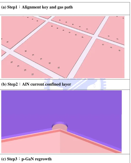
Fig. 3.6 Process flow chart of VCSELs from (a) to (n). ... 60
Fig. 3.7 Photography of VCSELs with incomplete isolation and surface were destroyed after laser liftoff. Silver regions are GaN material and yellow regions are contact metal which original covered by GaN but now exposed to air. ... 61
Fig. 3.8 SEM image of different apertures of SiO2 mask (a) 5 µm (b) 8µm (c) 10µm (d) 15µm ... 62
Fig. 3.9 SEM image of the SiO2 mask and the regrowth AlN layer ... 63
Fig. 3.10 The reflection spectrum of 10 pairs of TiO2 /SiO2 p-DBR ... 64
Fig. 3.11 Photography of VCSELs with p-contact layer and sapphire polish (a) front side (b) back side. ... 65
Fig. 3.12 PL spectrum before laser lift-off ... 66
Fig. 3.13 Photography of lift-off sapphire substrate ... 67
Fig. 3.14 OM image and roughness comparison from step 9 to step 11. ... 68
Fig. 3.15 Cross-sectional view and a top view before small mesa etching ... 69
Fig. 3.16 Photography of unwanted n-contact layer lifted off by PR stripper ... 70
Fig. 3.17 The reflection spectrum of 11 pairs of HfO2 /SiO2 n-DBR ... 71
ix
Fig. 3.19 AFM image of three different re-growth temperatures. ... 73
74 Fig. 3.21 The simulated reflectivity without n-DBR was deposited ... 74
Fig. 3.22 The PL spectrum before n-DBR was deposited ... 75
Fig. 3.23 The PL spectrum before n-DBR was deposited ... 76
Fig. 3.24 The light output power verse the pumping energy density ... 77
Fig. 3.25 The polarization characteristics of the laser emission from the VCSEL above the threshold. 77 Fig. 3.26 The logarithm light output power and laser emission peak linewidth verse the effective pumping energy density penetrating to QWs ... 79
Fig. 3.27 The electric field intensity simulated by transfer matrix, the horizontal axis correspond the layer arrangement of the VCSELs.... 79
Fig. 4.1 (a)The schematic representation of electron density wave propagating along a metal-dielectric interface (b) the electric field distribution around the interface (c) dispersion curve of surface plasmon ... 85
Fig. 4.2 A circular waveguide ... 87
Fig. 4.3 Bessel function of the first kind and second kind ... 89
Fig. 4.4 The lowest five modes and corresponding electric fields pattern E in circular waveguides ... 91
Fig. 4.5 The z-component magnetic field Hz and z-component poynting vector Pz for several TEnm modes ... 91
Fig. 4.6 Schematic of an nanolaser combining DBRs and metal ... 92
Fig. 4.7 The Quality factor distribution of different modes for an laser ... 93
Fig. 4.8 (a) Top view illustration of the structure (b) surface mode (c) hybrid mode (d) lowest four waveguide modes ... 94
Fig. 4.9 (a) Reflectivity and (b) absorptivity of common metal reflector ... 95
Fig. 4.10 (a) Real part of complex dielectric constant (b) n and k of common reflector ... 95
Fig. 4.11 Quality factor of (a) different metal (b) different thickness of Ag ... 96
Fig. 4.13 Cutoff wavelength of the structure ... 98
Fig. 4.15 (a) Quality factor, confinement factor and (b) threshold gain verse t height of InGaN/GaN quantum wells structure ... 99
Fig. 4.16 (a) Quality factor , confinement factor and (b) threshold gain verse diameter of InGaN/GaN quantum wells structure ... 100
Fig. 4.17 SEM image of bulk GaN rod before Al deposition ... 101
Fig. 4.18 PL spectrum and L.L curve of bare GaN rod with 1.2μm in height and 3.6μm in diameter. 102 Fig. 4 .19 PL spectrum and effective L.L curve of metal coated GaN rod with 1.2μm in height and 3.6μm in diameter. ... 102
10
Chapter 1
Introduction
1.1 Wide-bandgap III-V materials
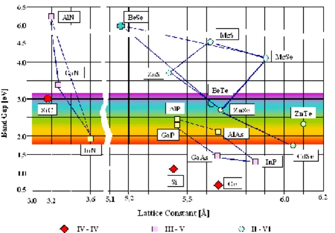
Wide-bandgap nitride materials have attracted great attention over past decade due to their promising potential for the applications of optoelectronic devices such as flat panel display, competing storage technologies, automobiles, general lighting, and biotechnology, and so on [1-4]. The III-N materials are synthesized mainly using the four kinds of atoms, gallium (Ga), nitride (N), aluminum (Al), and indium (In), to form the binary and ternary compounds such as GaN, InN, AlN, InxGa1-xN, and AlxGa1-xN etc. The bandgap of these materials cover a very wide range from 0.9eV to 6.1eV (Fig 1.1), which implies the large band off-set in hetero-structure could be achieved in this material system. The large band off-set is very useful to confine carrier for the high-speed and high power electronic devices and light emitting devices [5]. Their wide-range bandgap also provide possibility of full-color emission because they cover red, green, and blue emission regions. This property further makes nitride materials important and important for the applications of full-color display or solid-state lighting. Furthermore, nitride materials still have lots of advantages such as high bond energy (~2.3eV), high saturation velocity (~2.7 × 104 cm/s), high breakdown field (~2 × 10⁶ V/cm), and strong excitonic energy (>50meV) [6-7]. Although wurtzite nitride compounds have some unique properties such as piezoelectric field and spontaneous polarization which is harmful to the efficiency of light emitting devices, the material system still is a very strong candidate for the future optoelectronic applications due to their superior material properties.
11
Fig. 1.1 The band-gap diagram of Ⅱ - Ⅵ and Ⅲ - Ⅴ group semiconductor materials
1.2 Nitride-based Vertical Cavity Surface Emitting Lasers
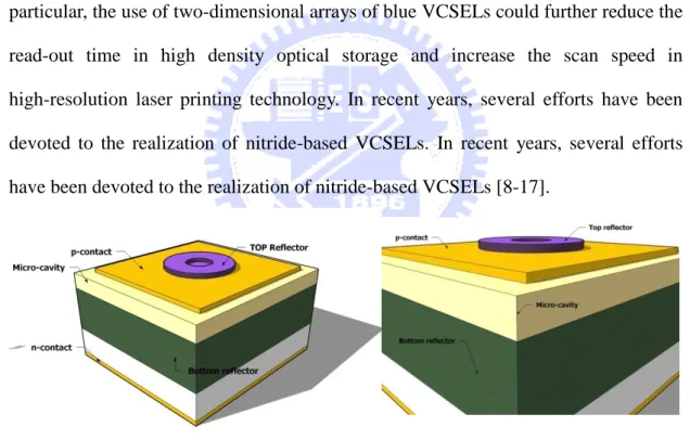
Although the optimization of the edge emitting laser keeps going, some properties of this kind of laser are unfavorable. One of those properties is its elliptic beam shape. On one hand, the coupling efficiency would be low as the elliptic beam is coupled into optical fiber (typically in the form of circular core). On the other hand, for the application of storage, the elliptic beam not only makes each writing pixel larger but also raises expenses for correcting light shape. Usually, this kind of laser shows slightly large divergence angle to be over ten degree. This also is disadvantageous to the projection. Furthermore, the side emitting laser devices also makes the testing of devices a tough task. The wafer should be cut into several stripes (several laser devices on one strip) before the testing. For a commercial product, the complicated testing would result in a poor producing efficiency and be disadvantageous. Therefore, in order to have a superior laser device, K. Iga demonstrated a new kind of laser diodes, vertical cavity surface emitting laser, in 1977. Vertical cavity surface emitting laser (VCSEL) is a vertical-emitting-type laser. It is formed by sandwiching a few-lambda cavity in a pair of reflectors, usually in the12
form of distributed Bragg reflector (DBR), with a very high reflectivity (>99.9%) as shown in Fig. 1.2. In contrast to EELs, photons in the cavity of VCSEL are vertically in resonance and emit outside perpendicularly to the surface of the structure. This laser diode can have many advantageous properties than conventional edge emitting laser, such as circular beam shape, lower divergence angle, two-dimensional laser array possible, efficient testing, low threshold, and so on. Owing to these superior performances, VCSELs had become very attractive and started to be applied to the commercial products at long wavelength range. In fact, short-wavelength VCSELs are also very promising for the applications of storage, display, and projection. In particular, the use of two-dimensional arrays of blue VCSELs could further reduce the read-out time in high density optical storage and increase the scan speed in high-resolution laser printing technology. In recent years, several efforts have been devoted to the realization of nitride-based VCSELs. In recent years, several efforts have been devoted to the realization of nitride-based VCSELs [8-17].
Fig. 1.2 The schematic diagram of a vertical-cavity surface emitting laser diode.
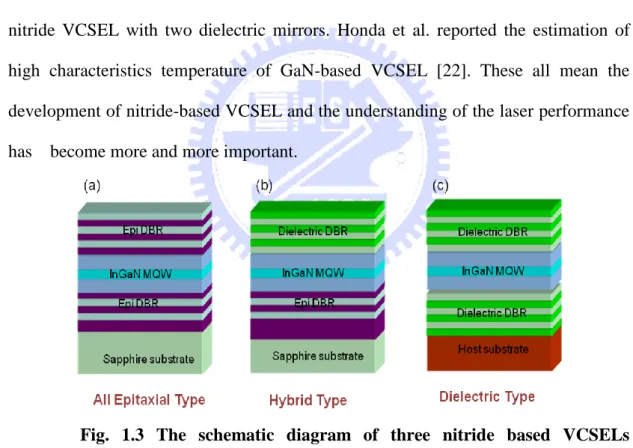
1.2.1 Fully Epitaxial Grown VCSELs
In 2005, J. F. Carlin [17] and E. Feltin [18] demonstrated the wholly epitaxial and high quality nitride-based micro-cavity (as shown in Fig. 1.3(a)) using
13
metalorganic vapor phase epitaxy (MOVPE or MOCVD). They used the lattice-matched AlInN/GaN as the bottom and top reflectors to avoid cracks happened due to the accumulation of the strain after stacking large pairs of layers. The reflectivity of AlInN/GaN could be achieved as high as 99.4%. They showed the 3/2-lambda cavity emitted a very narrow emission with a linewidth of 0.52 nm, corresponding to a quality factor of ~800.
1.2.2 VCSELs with Two Dielectric Mirrors
Compared to epitaxial grown reflectors, the fabrication of dielectric mirrors is relatively simple. Furthermore, the large index difference of dielectric mirrors makes them could easily have wide stop band (>50nm) and high reflectivity (>99%) by coating just few stacks of 1/4-lambda-thick layers. Therefore, using dielectric mirrors to accomplish nitride-based VCSELs had begun attractive. Song et al. [9], Tawara et al. [10] and J. T. Chu et. al [12]successively reported the structure (as shown in Fig. 1.3(c)) after 2000. They employed some process techniques such as wafer bonding and laser lift-off to make dielectric mirrors be coated onto both sides of nitride-based cavity. They showed a micro-cavity could have a very high quality factor to be greater than 400 and achieve lasing action using optical pumping. In addition, Takashi Mukai et al. [13] have demonstrated the CW lasing at room temperature in a GaN-based vertical-cavity surface-emitting laser (VCSEL) by current injection in 2008. Its optical cavity consisted of a 7λ-thick GaN semiconductor layer and an indium tin oxide layer for p-contact embedded between two SiO2/Nb2O5 dielectric distributed Bragg reflectors. The threshold current of
VCSEL is 13.9kA/cm2 and the lasing wavelength is about 414 nm. However, the fabrication technique of this kind of VCSEL is relatively complicated, and its cavity
14
length cannot be efficiently controlled due to polishing problems.
1.2.3 VCSELs with Hybrid Mirrors
The so-called hybrid mirrors are a combination of two different kinds of reflectors, for example, a dielectric mirror and an epitaxial reflector. Typically, the fabrication of this structure is to grow bottom reflector and cavity using MOCVD and then coat dielectric mirror to complete VCSEL structure (as shown in Fig. 1.3(b)). The hybrid-cavity nitride-based VCSEL\formed by the dielectric mirror and the epitaxially grown high-reflectivity GaN/AlxGa1-xN DBR was reported earlier. In
1999, Someya et al. [8] used 43 pairs of Al0.34Ga0.66N/GaN as the bottom DBR and
reported the lasing action at ~400nm. Then, Zhouet al. [11]also employed a bottom DBR of 60 pairs Al0.25Ga0.75N/GaN and observed the lasing action at 383.2nm. Both
these AlGaN/GaN DBR structures required large numbers of pairs due to the relatively low refractive index contrast between AlxGa1-xN and GaN. Therefore, recently some groups began to study the AlN/GaN for application in nitride VCSEL. The DBR structure using AlN/GaN has higher refractive index contrast (Δn/n=0.16) [19]that can achieve high reflectivity with relatively less numbers of pairs. It has wide stop band that can easily align with the active layer emission peak to achieve lasing action. However, the AlN/GaN combination also has relatively large lattice mismatch (~2.4%) and the difference in thermal expansion coefficients between GaN (5.59x10⁻⁶/K) and AlN (4.2x10⁻⁶/K) that tends to cause cracks in the epitaxial film during the growth of the AlN/GaN DBR structure and could result in the reduction of reflectivity and increase in scattering loss. With the mature of epitaxy techniques, the high-reflectivity AlN/GaN DBR structure with relatively smooth surface morphology has become possible with just twenty or thirty pairs [20]. In
15
comparison of these three VCSELs, it doesn’t require complicated process such as laser lift-off technique to complete a hybrid VCSEL device. This means the fabrication of such structure is stable and reliable comparing to other structures. Thus, the hybrid structure is more advantageous in the aspects of fabrication and commercialization In fact, the investigation of the characteristics of the GaN-based VCSELs has gradually attracted more attentions. Kako et al. [21]investigated the coupling efficiency of spontaneous emission (β) and the polarization property of the nitride VCSEL and obtained a high β value of 1.6×10⁻²
and a strong linear polarization of 98%. Tawara et al. [10]also found a high β value of 10-2 in the nitride VCSEL with two dielectric mirrors. Honda et al. reported the estimation of high characteristics temperature of GaN-based VCSEL [22]. These all mean the development of nitride-based VCSEL and the understanding of the laser performance has become more and more important.
Fig. 1.3 The schematic diagram of three nitride based VCSELs structures
1.3 Nanolasers
Nanolasers [23] refer generally to miniaturized lasers that have sizes comparable to or smaller than wavelength involved. The driving force behind the development of
16
nanolasers, is the well-recognized sizemismatch between silicon-based microelectronic devices and the compound-semiconductor-based optoelectronic devices. As is evidenced by Moore’s law for microelectronics, miniaturization and large-scale integration can lead to drastic improvement of performance and simultaneous decrease in cost. Efforts in integrated photonics over the last few decades have led to much less impressive results than electronic integrated circuits (ICs). Several of paradigm-shifting approaches in the last decade have resulted in record size reduction of microcavity lasers. These new approaches are best represented by the microdisk lasers supported on a pedestal [24–26], the photonic wire lasers [27] and photonic crystal (PC) lasers [28–31]. The high quality-factor cavity provided by the whisper-ing-gallery modes in microdisk lasers allows the gain volume to be reduced to the minimum. Similarly, high quality factor provided by photonic bandgap structures leads to a record size in optical mode volume. While the vertical size of disk and PC laser structures is sub-wavelength already, the lateral size is still comparably larger, on the order of 10 m. Notice that at 2011, Roger Chen et al. [32] use a novel growth scheme to directly demonstrate the potency of bottom-up nano-optoelectronic integration of InGaAs nanopillar lasers. As show in Fig. 1.4, unique helically propagating cavity modes are used to strongly confine light despite the low refractive index contrast between InGaAs and silicon. Finally, all but one [28] of these lasers are so far optically pumped, whereas eventual device integration requires electrical injection lasers.
17
Fig. 1.4 (a) Schematic of a nanopillar laser monolithically integrated onto silicon. (b) SEM image showing the well-faceted geometry of the nanopillar optical cavity. (c) First-order and (d) higher-order standing waves
1.3.1 Metal Coated Nanolasers
Metal coated cavity has been intensely researched by scientist around the world. It could reduce the size o semiconductor laser to nano scale, even in subwavlentgh scale. This result breaks the diffraction limit which constrains the size of a laser that cannot be smaller than its nature wavelength. The lasing characteristics also be studied by researchers trying to explain the physical meaning.
As shown in Fig. 1.5 , Marin T. Hill et al. [33][34] demonstrated lasing in metal-coated nanocavity at 2007 and 2009. They coated silver and dielectric layer on the nanorod and observe lasing signal at 77K. After that, different designs of metal-coated nanocavtiy have reported experimentally or theoretically. Moreover, different kinds of metal have been use to form metal-coated nano cavity. From recent research results [33-37], researcher use silver, gold and aluminum to from the nano structure. At 2010, M. P. Nezhad et al. demonstrated a metal coated nanocavity with aluminum layer and SiO2 as the dielectric layer. They also proposed a theoretical analysis to show that optimization of the dielectric layer could have a higher chance to
18
get a better quality factor to achieve lasing action. K. Y. Yu et al. at 2010 demonstrated a nano-patch laser with metal coated above and below the gain medium, and analyze the lasing characteristic of the device [36]. In 2011, M. W. Kim et al. demonstrated lasing in metal-clad microring [37]. In summary, metal-coated nano cavity has been demonstrated experimentally in different structures includes nanorod , waveguide, and ring. In sum, recent research results mainly focus on InGaAsP material system, which has a lasing wavelength from red to infared region.
Fig. 1.5 The structure of cavity formed by a rectangular semiconductor pillar encapsulated in Silver. (a) The schematic showing the device layer structure. (b) the scanning electron microscope image showing the semiconductor core of one of the devices. The scale bar is 1 micron.
1.3.2 Metal Coated Nanolasers with Surface Plasmon Effects
At 2008, metal-coated waveguide structure had been demonstrated and bow-tie nanostructure had been demonstrated by S. W. Chang et al. [38]. The combination of surface plasmon effect and bow-tie structure shows a promising way theoretically in forming a semiconductor. At 2009 and 2011, Oulton group [39][40] report the experimental demonstration of nanometre-scale plasmonic lasers, generating optical modes a hundred times smaller than the diffraction limit. They realize such lasers using a hybrid plasmonic waveguide consisting of a high-gain cadmium sulphide
19
(CDS) semi-conductor nanowire, separated from a silver surface by a 5nm thick insulating gap. As shown in Fig. 1.6, Gwo group [41][42] demonstrated the 3D subdiff raction-limited laser operation in the green spectral region based on a metal-oxide- semiconductor (MOS) structure and use atomically smooth epitaxial Ag on Si as a improvement for plasmonics at 2011 and 2012.
Fig. 1.6 (A) Schematic of device: a single nanorod on a SiO2 covered
epitaxial Ag film (28 nm thick). The energy-density distribution (right) is calculated by the eigenmode method. (B) SEM images of nanorods. The left-hand SEM image shows the actual nanorod on epitaxial Ag film (C) STEM and TEM structural analyses
1.4 Motivation & Objective of the Thesis
Our group reported room-temperature CW lasing of a GaN-based VCSEL with a bottom AlN/GaN DBR epitaxially grown on a sapphire substrate, a top dielectric DBR, and side-by-side n- and p-type contacts. And we also reported CW lasing both at 77 K and room temperature. However, the diffculty in obtaining high quality quantum wells (QWs) on such an epitaxial DBR and the heat generation induced by
20
current crowding in the side-by-side configuration still wait to be resolved. In this research, we utilize wafer bonding and laser liftoff techniques to permit VCSELs to be fabricated between two dielectric DBRs in a vertical contact structure, which improves the reflectivities of the DBRs , the current crowding effect and thermal dissipation. Besides, we add a unique AlN layer for current and optical confinement further improvement.
Metal-coated nanocavity shows huge potential to reduce the size of semiconductor laser into subwavelength scale. However, their research results mainly focus on InGaAsP material system and optical communication to infrared wavelength region. Shorter lasing wavelength and other material system have seldom been discovered by other groups in the world. The certified phenomena explanation and optimized design rule for metal-coated nanocavity is not clear. In this research, we utilize GaN as the gain medium for metal- coated nanocavity, combining with DBRs and silicon oxide. We try to clarify some myth for metal-coated nanocavity design. Finally, we design a minimum structure which is feasible and possible for laser operation.
The primary objective of this thesis focus on the development of GaN-based two dielectric VCSELs and the design of GaN-based metal-coated nanolaser. In chapter 2, we briefly introduce the instruments、process parameters and techniques which are used to fabricate and measure the devices. In chapter 3, we present experiments and results of lasing in AlN layer VCSELs at room temperature. In chapter 4, we use finite element method and circular waveguide theory to design a metal- coated
nanolaser and shows some of preliminary results. Finally in chapter 5, we give a brief conclusion of this thesis.
21
Reference
[1] S. Nakamura, M. Senoh, N. Iwasa, and S. Nagahama, Jpn. J. Appl.Phys., 34, L797 (1995)
[2] S. Nakamura, T. Mukai, and M. Senoh, Appl. Phys. Lett.,64, 1687 (1994)
[3] S. Nakamura, M. Senoh, S.Nagahama, N.Iwasa, T. Yamada, T. Matsushita, Y. Sugimoto,and H.Kiyoku, Appl. Phys. Lett., 70, 868 (1997)
[4] S. Nakamura, Science, 281, 956 (1998)
[5] Y. Arakawa, IEEE J. Select. Topics Quantum Electron., 8, 823 (2002)
[6] H. Morkoc, Nitride Semiconductors and Devices (Spring Verlag, Heidelberg) (1999)
[7] S. N. Mohammad, and H. Morkoc, Progress in Quantum Electron., 20, 361 (1996) [8] T. Someya, R.Werner, A. Forchel, M. Catalano, R. Cingolani, Y.Arakawa,
Science, 285,1905 (1999)
[9] Y.-K. Song, H. Zhou, M. Diagne, A. V. Nurmikko, R. P. Schneider, Jr., C. P. Kuo, M. R. Krames, R. S. Kern, C. Carter-Coman, and F. A. Kish, Appl. Phys. Lett., 76, 1662 (2000)
[10] T. Tawara, H. Gotoh, T. Akasaka, N. Kobayashi, and T. Saitoh, Appl. Phys. Lett., 83, 830 (2003)
[11] H. Zhou, M. Diagne, E. Makarona, A. V. Nurmikko, J. Han, K. E. Waldrip and J. J. Figiel, Electron. Lett., 36,1777 (2000)
[12] J.T. Chu et. al., Jpn. J. Appl. Phys, 45, 2556 (2006).
[13] Yu Higuchi, Kunimichi Omae , Hiroaki Matsumura, and Takashi Mukai Applied Physics Express 1 , 121102 (2008)
22
[15]. C. C. Kao et. al., Appl. Phys. Lett., 87, 081105-1 (2005). [16] C. C. Kao et. al., IEEE Photon. Technol. lett., 18, 877 (2006).
[17] J. F. Carlin, J. Dorsaz, E. Feltin, R. Butté, N. Grandjean, M. Ilegems, and M. Laügt, Appl.Phys. Lett., 86, 031107 (2005)
[18] E. Feltin, R. Butté, J. F. Carlin, J. Dorsaz, N. Grandjean, and M. Ilegems, Electron. Lett.,41, 94 (2005)
[19] T. Ive, O. Brandt, H. Kostial, T. Hesjedal, M. Ramsteiner, and K. H. Ploog, Appl. Phys. Lett., 85, 1970 (2004)
[20] H.H. Yao, C.F. Lin, H.C. Kuo, S.C. Wang, J. Crystal Growth, 262, 151 (2004) [21] S. Kako, T. Someya, and Y. Arakawa, Appl. Phys. Lett., 80, 722 (2002)
[22] T. Honda, H. Kawanishi, T. Sakaguchi, F. Koyama and K. Iga, MRS Internet J. Nitride Semicond. 4S1, G6.2-1 (1999).
[23] Ning, C. Z. physica status solidi (b), NA-NA, doi:10.1002/pssb.200945436 (2010).
[24] A. F. Levi, S. L. McCall, S. J. Pearton, and R. A. Logan, IEEE Electron. Lett. 29, 1666 (1993).
[25] T. Baba, M. Fujita, A. Sakai, M. Kihara, and R. Watanabe, IEEE Photon. Technol. Lett. 9, 878 (1997).
[26] K. Srinivasan, M. Borcelli, O. Painter, A. Stintz, and S. Krishna, Opt. Express 14, 1094 (2006).
[27] J. P. Zhang, D. Y. Chu, S. L. Wu, S. T. Ho, W. G. Bi, C. W. Tu, and R. C. Tiberio, Phys. Rev. Lett. 75, 2678 (1995).
[28] H. Park, S. Kim, S. Kwon, Y. Ju, J. Yang, J. Baek, S. Kim, and Y. H. Lee, Science 305, 1444 (2004).
23
Noda, Opt. Express 15, 17248 (2007).
[30] A. J. Danner, J. C. Lee, J. J. Raftery, Jr., N. Yokouchi, and K. D. Choquette, Electron. Lett. 39, 1323 (2003).
[31] K. Nozaki, H. Watanabe, and T. Baba, Appl. Phys. Lett. 92, 021108 (2008). [32] Chen, R., Tran, T. T. D., Ng, K. W., Ko, W. S., Chuang, L. C., Sedgwick, F. G.,
Chang-Hasnain, C., Nat. Photonics, vol5, March 2011.
[33] Hill, M. T., Marell, M., Leong, E. S. P., Smalbrugge, B., Zhu, Y. C., Sun, M. H., van Veldhoven, P. J., Geluk, E. J., Karouta, F., Oei, Y. S., Notzel, R.
Ning, C. Z., Smit, M. K. “L, Nat. Photonics, vol. 1, pp. 589, 2007.
[34] Hill, M. T. et al. o62Lasing in metal-insulator-metal sub-wavelength plasmonic waveguides. Opt. Express 17, 11107-11112 (2009).
[35] Nezhad, M. P., Simic, A., Bondarenko, O., Slutsky, B., Mizrahi, A., Feng, L. A., Lomakin, V., Fainman, Y., Nat. Photonics, vol. 4, pp. 395, 2010.
[36] Yu, K., Lakhani, A. Wu, M. C., Opt. Express, vol. 18, pp. 8790, 2010 [37] M. W. Kim, P. C. Ku, Appl. Phys. Lett., vol. 98, pp. 131107, 2011.
[38] Chang, S. W., Ni, C. Y. A., Chuang, S. L., Opt. Express, vol. 16, pp. 10580, 2008
[39] Oulton, R. F. et al. doi:10.1038/nature08364 (2009).
[40] Sorger, V. J. et al. Nature communications 2, 331, doi:10.1038/ncomms1315 2011.
[41] Wu, C. Y. et al. Nano Lett 11, 4256-4260, doi:10.1021/nl2022477 (2011). [42] Lu, Y. J. et al. P. Science 337, 450-453, doi:10.1126/science.1223504 (2012).
24
Chapter 2
Numerical Methods, Fabrication Instruments,
Measurement Setups and Process Parameters
2.1 Numerical Simulation Methods
2.2.1 Transfer Matrix Method
The transfer-matrix method [1] is a method used in optics and acoustics to analyze the propagation of electromagnetic or acoustic waves through a stratified (layered) medium [2]. This is for example relevant for the design of anti-reflective coatings and dielectric mirrors.
The reflection of light from a single interface between two media is described by the Fresnel equations. However, when there are multiple interfaces, such as in the figure, the reflections themselves are also partially transmitted and then partially reflected. Depending on the exact path length, these reflections can interfere destructively or constructively. The overall reflection of a layer structure is the sum of an infinite number of reflections, which is cumbersome to calculate.
The transfer-matrix method is based on the fact that, according to Maxwell's equations, there are simple continuity conditions for the electric field across boundaries from one medium to the next. If the field is known at the beginning of a layer, the field at the end of the layer can be derived from a simple matrix operation. A stack of layers can then be represented as a system matrix, which is the product of the individual layer matrices. The final step of the method involves converting the system matrix back into reflection and transmission coefficients.
25
2.2.2 Finite Element Method
The finite element method (FEM) [3] is a method used for finding the approximate solution of partial differential equations (PDE) that handle complex geometries (and boundaries), such as waveguides with arbitrary cross-sections, with relative ease. The field region is divided into elements of various shapes, such as triangles and rectangles, allowing the use of an irregular grid. The solution approach is based either on eliminating the differential equation completely (steady state problems), or rendering the PDE into an equivalent ordinary differential equation, which is then solved using standard techniques, such as finite differences. In a context of optical waveguides, the FEM can be used for mode solving and propagation problems. Two approaches to solve waveguide problem include the variational method and the weighted residual (Galerkin) method. Both methods lead to the same eigenvalue equation that needs to be solved.
Fig. 2.1 Commercial Software of transfer matrix method (TFCalc 3.5) and finite element method (COMSOL 4.2)
2.2 Fabrication Instruments
2.2.1 Electron-Beam Lithography System
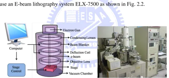
Electron beam lithography, usually call as E-beam lithography, is a technique to utilize a beam of electrons to exposing the photo resist on the surface of a material, then selectively removing the photo resist on the film to transfer the pattern we want
26
onto the film. This could break the diffraction limit which constrains conventional photo lithography technique, and shows a promising chance to fabricate device in nano-scale.
The E-beam lithography system usually consists of an electron gun as source of electron, lenses for focusing, stage for moving the sample precisely under the electron beam, a beam blanker to control the exposure time of electron beam and a computer to control the whole system and the pattern. Fig. 2.2 shows the schematic diagram. For most of E-beam lithography system used for commercial applications are very expensive; therefore, for academic purpose, people usually convert an electron microscope into an E-beam lithography system with a relatively low cost. For thesis, we use an E-beam lithography system ELX-7500 as shown in Fig. 2.2.
Fig. 2.2 Schematic diagram of e-beam lithography and E-beam Lithography System (ELX-7500)
2.2.2 Mask Alignment and Exposure System
Photolithography (also termed "optical lithography" or "UV lithography") [4] is a process used in microfabrication to selectively remove parts of a thin film or the bulk of a substrate. It uses light to transfer a geometric pattern from a photomask to a light-sensitive chemical "photoresist", or simply "resist," on the substrate. A series of
27
chemical treatments then either engraves the exposure pattern into, or enables deposition of a new material in the desired pattern upon, the material underneath the photo resist. For example, in complex integrated circuits, a modern CMOS wafer will go through the photolithographic cycle up to 50 times.
Photolithography shares some fundamental principles with photography in that the pattern in the etching resist is created by exposing it to light, either directly (without using a mask) or with a projected image using an optical mask. This procedure is comparable to a high precision version of the method used to make printed circuit boards. Subsequent stages in the process have more in common with etching than with lithographic printing. It is used because it can create extremely small patterns (down to a few tens of nanometers in size), it affords exact control over the shape and size of the objects it creates, and because it can create patterns over an entire surface cost-effectively. Its main disadvantages are that it requires a flat substrate to start with, it is not very effective at creating shapes that are not flat, and it can require extremely clean operating conditions.
Fig. 2.3 Simplified illustrations of dry etching using positive photoresist during a photolithography process in semiconductor micro-fabrication.
28
Fig. 2.4 Alignment System (ABM Model 60 DUV/MUV/NearUV)
2.2.3 Plasma-Enhanced Chemical Vapor Deposition (PECVD)
Plasma-enhanced chemical vapor deposition (PECVD) [5] is a process used to deposit thin films from a gas state (vapor) to a solid state on a substrate. Chemical reactions are involved in the process, which occur after creation of a plasma of the reacting gases. The plasma is generally created by RF frequency between two electrodes, the space between which is filled with the reacting gases. Silicon dioxide can be deposited using a combination of silicon precursor gasses like dichlorosilane or silane and oxygen precursors, such as oxygen and nitrous oxide, typically at pressures from a few millitorr to a few torr. Plasma-deposited silicon nitride, formed from silane and ammonia or nitrogen, is also widely used, although it is important to note that it is not possible to deposit a pure nitride in this fashion. Plasma nitrides always contain a large amount of hydrogen. Fig.2.5 shows the Plasma-enhanced chemical vapor deposition system used to deposit SiNx or SiO2 as
29
Fig. 2.5 Plasma Enhanced CVD System (SAMCO PECVD Model PD-220)
2.2.4 Electron Beam Physical Vapor Deposition
Electron Beam Physical Vapor Deposition [6] is a form of physical vapor deposition in which a target anode is bombarded with an electron beam given off by a charged tungsten filament under high vacuum. The electron beam causes atoms from the target to transform into the gaseous phase. These atoms then precipitate into solid form, coating everything in the vacuum chamber (within line of sight) with a thin layer of the anode material.
Thin film deposition is a process applied in the semiconductor industry to grow electronic materials, in the aerospace industry to form thermal and chemical barrier coatings to protect surfaces against corrosive environments, in optics to impart the desired reflective and transmissive properties to a substrate and elswhere in industry to modify surfaces to have a variety of desired properties. The deposition process can be broadly classified into physical vapor deposition (PVD) and chemical vapor deposition (CVD). In CVD, the film growth takes place at high temperatures, leading to the formation of corrosive gaseous products, and it may leave impurities in the film. The PVD process can be carried out at lower deposition temperatures and without
30
corrosive products, but deposition rates are typically lower. Electron beam physical vapor deposition, however, yields a high deposition rate from 0.1 μm / min to 100 μm / min at relatively low substrate temperatures, with very high material utilization efficiency. The schematic of an EBPVD system is shown in Fig. 2.6.
Fig. 2.6 Simplified illustration of e-beam evaporator
Fig. 2.7 Coating system with optical in-situ monitor (KS-800OPTO) and E-gun evaporator (ULVAC EBX-8C)
2.2.5 Dry Etching System
31
their plan, and there are two types of etching processes: wet etching and dry etching. Dry etching process uses plasma to etch the semiconductor material and it is a kind of anisotropic etching process. The line-width of dry etching process is smaller than wet etching, therefore, dry etching process gradually replace wet etching process after 1980.
The mechanism of dry etching process is as follow: first, the etching gas has been diffuse to chamber under ultra-low pressure. Second, when the pressure is stable, plasma is produced by RF frequency. Third, the radicals produced by bombardment of high speed electron would diffuse to the wafer and attach to its surface. Fourth, with the help of ion bombardment, these radicals would react with the atoms on the surface and form by-product as gas. At the end, these volatile by-products would then leave the surface of wafer and discharge from chamber. Fig. 2.8 shows the inductively coupled plasma and reactive ion etching (ICP-RIE) system used to etch Si3N4 layer to
transfer the patter from PMMA layer, and the ICP-RIE equipment used to etch GaN layer.
Fig. 2.8 ICP-RIE System (Oxford Plasmalab System 100) and ICP-RIE System (SAMCO RIE-101PH).
32
2.3 Measurement Setups
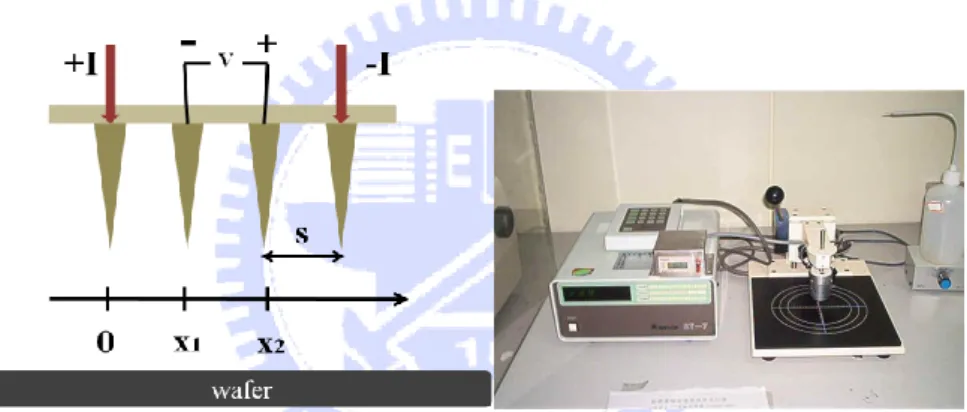
2.3.1 Four Point Probe
The 4-point probe setup consists of four equally spaced tungsten metal tips with finite radius. Each tip is supported by springs on the other end to minimize sample damage during probing. The four metal tips are part of an auto-mechanical stage which travels up and down during measurements. A high impedance current source is used to supply current through the outer two probes; a voltmeter measures the voltage across the inner two probes (See Fig. 2.9) to determine the sample resistivity. Typical probe spacing is ~ 1 mm.
Fig 2.9 Schematic of 4-point probe configuration and Four point probe system (NAPSON RT-7)
2.3.2 Scanning Electron Microscopy (SEM)
Scanning electron microscope (SEM) is one of the most important equipment for people to observe objects in nano-scale. The electrons interact with atoms that make up the sample producing signals that contain information’s about itself. Moreover, preparation of the samples for SEM is relatively easy due to the fact that SEM only require the sample to be conductivity. The combination of higher magnification, larger depth of focus, greater resolution, and ease of sample observation makes the SEM becomes one of the most widely used equipment used for commercial and research
33
purposes. Fig. 2.10 shows the JSM-7000F made by JEOL.
.
Fig. 2.10 Scanning electron microscope System (JSM-7000F)
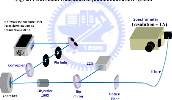
2.3.3 Photoluminescence Spectroscopy (PL)
Photoluminescence characterization equipment generally uses the PL method to obtain the wavelength and intensity of the semiconductor material being analyzed. PL is the process of optical absorption of electrons in solids between an initial energy state Ei and a final energy state Ef. Excitation of an electron to Ef will leave Ei
unoccupied creating a hole. Absorption creates electron-hole pairs while luminescence is the process which occurs when electrons in excited states drop to a lower level emitting a photon ħw as shown in Fig. 2.11. The electron–hole recombination creates a photon which is also known as a radiative transition. Direct gap materials are good light emitters and their optical properties are analyzed using this technique.
Photons are absorbed using an excitation source which is typically a laser. The frequency of the source ħwL must be greater than the energy gap Eg. The result is that electrons are injected into the conduction band and holes into the valence band. Electrons and holes are initially created in higher states within these bands but will rapidly relax to the bottom of their respective bands reaching their lowest energy state. Relaxation occurs by emitting phonons, for energy loses from the higher states,
34
which obeys the conservation laws. The difference in energy between the two bands is Eg which is the energy gap, also known as the band gap. Luminescence occurs close to the band gap Eg, near k = 0. After excitation, both electrons and holes relax to their lowest energy states by emitting phonons.
Fig. 2.11 Interband transitions in photoluminescence system
Fig. 2.12 The optical pumping system in experiment Using Nd:YVO4 355 nm pulse laser as pumping source, the pulse width is 0.5 ns, and repetition rate is 1k Hz. The laser light is focused by convex lens and pumped onto the device. Use objective lens to receive the light which emit from the device, and take flip mirror to control the optical path transmitting to CCD or fiber.
35
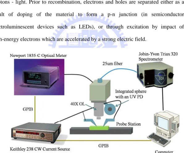
2.3.4 Electroluminescence Spectroscopy (EL)
As shown in Fig. 2.13, Electroluminescence (EL) is an optical phenomenon and electrical phenomenon in which a material emits light in response to an electric current passed through it, or to a strong electric field. This is distinct from light emission resulting from heat (incandescence), chemical reaction (chemiluminescence), sound (sonoluminescence), or other mechanical action (mechanoluminescence). Electroluminescence is the result of radiative recombination of electrons and holes in a material (usually a semiconductor). The excited electrons release their energy as photons - light. Prior to recombination, electrons and holes are separated either as a result of doping of the material to form a p-n junction (in semiconductor electroluminescent devices such as LEDs), or through excitation by impact of high-energy electrons which are accelerated by a strong electric field.
Fig. 2.13 The EL measurement system for electrically driving
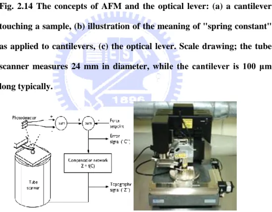
2.3.5 Atomic Force Microscope (AFM)
36
scan. In the case of the AFM, the probe is a tip on the end of a cantilever which bends in response to the force between the tip and the sample. The small probe-sample separation (on the order of the instrument's resolution) makes it possible to take measurements over a small area. To acquire an image the microscope raster-scans the probe over the sample while measuring the local property in question.
The resulting image resembles an image on a television screen in that both consist of many rows or lines of information placed one above the other. Unlike traditional microscopes, scanned-probe systems do not use lenses, so the size of the probe rather than diffraction effect generally limits their resolution. As shown in Fig. 2.14 AFM operates by measuring attractive or repulsive forces between a tip and the sample. In its repulsive "contact" mode, the instrument lightly touches a tip at the end of a leaf spring or "cantilever" to the sample. As a raster-scan drags the tip over the sample, some sort of detection apparatus measures the vertical deflection of the cantilever, which indicates the local sample height. Thus, in contact mode the AFM measures hard-sphere repulsion forces between the tip and sample. In tapping mode, the AFM derives topographic images from measurements of attractive forces; the tip does not touch the sample.
The presence of a feedback loop is one of the subtler differences between AFMs and older stylus-based instruments such as record players and stylus profilometers. The AFM not only measures the force on the sample but also regulates it, allowing acquisition of images at very low forces. As shown in Fig. 2.15, the feedback loop consists of the tube scanner that controls the height of the entire sample; the cantilever and optical lever, which measures the local height of the sample; and a feedback circuit that attempts to keep the cantilever deflection constant by adjusting the voltage applied to the scanner. One point of interest: the faster the feedback loop can correct
37
deviations of the cantilever deflection, the faster the AFM can acquire images; therefore, a well-constructed feedback loop is essential to microscope performance. AFM feedback loops tend to have a bandwidth of about 10 kHz, resulting in image acquisition time of about one minute.
Fig. 2.14 The concepts of AFM and the optical lever: (a) a cantilever touching a sample, (b) illustration of the meaning of "spring constant" as applied to cantilevers, (c) the optical lever. Scale drawing; the tube scanner measures 24 mm in diameter, while the cantilever is 100 μm long typically.
Fig. 2.15 The AFM feedback loop. A compensation network monitors the cantilever deflection and keeps it constant by adjusting the height of the sample. Atomic Force Microscope(D3100)
38
2.3.6 Others
Fig. 2.16 N&K Surface Profile Analyzer (N&K 1500)
2.4 Fabrication Process Parameters and Techniques
To fabricate GaN-based light emitting devices, there are some useful parameters and techniques used in our experiments regularly. And also those information will be mention and quote in second half of this thesis.
2.4.1 Initial Clean (I.C.)
The purpose of Initial Clean (I.C.) is to remove the small particle and organism on the sample surface. You should do it before each fabrication process. The details parameters are expressed as below:
1. Degreasing particles in acetone (ACE) 5min by ultrasonic baths.
2. Dipping in isopropyl alcohol (IPA) 5min by ultrasonic baths for organism removed.
3. Rising in de-ionized water (D.I. water) 5min for surface clean. 4. Blowing with N2 gas for surface drying.
39
2.4.2 Lithography Techniques and Parameters
The purpose of the photolithography is to transfer the pattern of the mask to the photoresist (PR) on the wafer. In our experiments, positive photoresists AZ-6112、 AZ-5214E and negative photoresists AZ-2020 、 AZ-2070 were used. Although AZ-5214E is positive photoresist, it is capable of image reversal (IR) resulting in the effect of negative photoresist. In fact AZ-5214E is almost exclusively used in the IR-mode which is proper to be used in the lift-off process. However, image reversal resists generally do not cross-link. Hence, from approx. 120-130°C on, the resist structures start to soften. The solution is AZ-2020 which has approximate thickness and stronger mechanical properties. AZ-2070 is used when we need extreme thickness photoresist mask. Notice that hard bake 120
o
C 5min can be applied when dry etching is the following process. Those photolithography techniques are described as below:
AZ-6112 positive exposure
Initial Clean Dehydration Bake
120
o
C 5min
Spin coating 1000rpm/10sec, 3000rpm/30sec (thickness ~2μm) Soft bake
90
o
C 90sec
Edge bead removal Polyester swab moisten with ACE. Alignment and exposure 1.9sec ~ 2.2sec
Development Dip in AZ-300 30sec、Water 30sec
Post check OM.
Hard bake
120
o
40
AZ-5214E image reverse exposure
Initial Clean Dehydration Bake
120
o
C 5min
Spin coating 1000rpm/10sec, 3000rpm/30sec (thickness ~1.6μm) Soft bake
90
o
C 90sec
Edge bead removal Polyester swab moisten with ACE. Alignment and exposure 2.8sec ~ 3 sec
Reversal bake
120 oC 120sec Flood exposure 11sec ~ 13sec
Development Dip in AZ-300 40sec、Water 30sec
Post check OM.
Hard bake
120
o
C 5min (optional)
AZ-2020 negative exposure
Initial Clean Dehydration Bake
120
o
C 5min
Spin coating 1000rpm/10sec, 1500rpm/35sec (thickness 2 ~3μm) Soft bake
110
o
C 60sec
Edge bead removal Polyester swab moisten with ACE. Alignment and exposure 100mJ/cm2
Post bake
41
Development Dip in AZ-300 120sec、Water 30sec
Post check OM.
Hard bake
120
o
C 5min (optional)
AZ-2070 negative exposure
Initial Clean Dehydration Bake
120
o
C 5min
Spin coating 1000rpm/10sec, 2200rpm/30sec (thickness 6~7μm) Soft bake
110
o
C 120sec
Edge bead removal Polyester swab moisten with ACE Alignment and exposure 16sec ~ 19sec
Post bake
110 oC 140sec
Development Dip in AZ-300 120sec、Water 30sec
Post check OM.
Hard bake
120
o
C 5min (optional)
2.4.3 PECVD Deposition Techniques and Parameters
The purpose of PECVD technique is to deposit a Si3N4 film for hard mask. The
details of PECVD parameters are as shown below:
Si3N4 film deposition (SAMCO PD220) SiH4/Ar: 20sccm
Temperature: 300
o
C Rate: 9.6nm/min NH3: 10sccm RF power: 35W
42
N2: 490sccm Pressure: 100Pa
SiO2 film deposition (OXFORD INSTRUMENTS Plasmalab80Plus)
SiH4: 9sccm Temperature: 300 o C Rate: 81nm/min N2O: 710sccm RF power: 25W Pressure: 1000mTorr
2.4.4 Dry Etching Techniques and Parameters
Dry etching provide anisotropic etching extensively used in mask transferation. Noticed that dry etching also cause critical sidewall roughness. The ICP-RIE parameters are as shown below:
Si3N4 film etching (Oxford Plasmalab system 100)
Ar/O2: 5sccm Temperature: 20℃ Rate: 90nm/min
CHF3: 50sccm RF power: 150W
Pressure: 7.5*10-9Torr
GaN film etching (SAMCO RIE-101PH)
Ar: 20sccm Temperature: 20℃ Rate: 660nm/min
Cl2: 40sccm ICP power: 200W
Bias power: 200W Pressure: 0.49Pa
43
2.4.5 Polish techniques
Diamond lapping films usually used in polishing fiber optic connectors. The mineral key on films make from aluminum oxide or diamond which supperizely has good perfomace in elimitating the GaN surface roughness caused by dry etching .
Fig. 2.17 Photography of diamond lapping films
2.4.6 Lift-off techniques with photoresists
Beside wet or dry etching, lift-off is a common technique to pattern metal or dielectrica films in the µm or sub-µm range. The main criteria for the choice of a photoresist best-suited for a certain lift-off process are:„
● The thickness of the coated material
● The coating technology (evaporation, sputtering, CVD, ...) and the maximum temperature the resist film has to stand during coating
● The required resolution
Generally, the thickness of photoresist has to be three times thicker than the coating film and can be remove easily by ACE with ultrasonic vibration in several minutes at room temperature. For some difficult cases, the used of thicker photoresist、PR stripper、higher solvent temperature、strogher ultrasonic intensity can accelerate lift-off process.
44
Reference
[1] http://en.wikipedia.org/wiki/Transfer-matrix_method_%28optics%29
[2] Born, M.; Wolf, E., Principles of optics: electromagnetic theory of propagation, interference and diffraction of light. Oxford, Pergamon Press, 1964.
[3] http://optical-waveguides-modeling.net/index.jsp
[4] http://en.wikipedia.org/wiki/Photolithography
[5] http://en.wikipedia.org/wiki/Plasma-enhanced_chemical_vapor_deposition [6] http://en.wikipedia.org/wiki/Electron_beam_physical_vapor_deposition
45
Chapter 3
An AlN Layer for the Current Confinement in
GaN-Based VCSELs with Two Dielectric Distributed
Bragg Reflectors
3.1 Operation principle of VCSELs
3.1.1 Fabry–Pérot cavity
The most common types of optical cavities consist of two facing plane (flat) or spherical mirrors [1]. The simplest of these is the plane-parallel or Fabry–Pérot cavity, consisting of two opposing flat mirrors. In basics of laser physics a laser cavity where a propagating mode has to be stationary inside the cavity to form a laser as shows in Fig. 3.1. Mathematically this means that a complex field amplitude, E0 at an arbitrary
location inside the cavity has to return to the original value after a round trip propagation and twice of reflections at the two-end facets, or
r
1r
2exp{2ikL} E
0= E
0 (3.1) where r1 , r2 ,k are amplitude reflectivities of the two facets and complex propagationconstant, respectively. Splitting Equation above into real and imaginary parts leads to following two equations k = k k :
=
ln r1r22k (3.1)
=
2
= 2
(3.2)By Eq. 3.2 and mathematical derivation, the mode spacing can be given as
=
2 246
Fig. 3.1 Schematic of a laser cavity showing the length, L, and reflection coefficients of the two-end facets, r1 and r2.
3.1.2 Characteristics of Distributed Bragg reflectors (DBR)
Distributed Bragg reflectors (DBR) serve as high reflecting mirror in numerous optoelectronic and photonic devices such as VCSEL. There are many methods to analyze and design DBRs, and the matrix method is one of the popular one. The calculations of DBRs are entirely described in many optics books, and the derivation is a little too long to write in this thesis. Hence, we put it in simple to understand DBRs. Consider a distributed Bragg reflector consisting of m pairs of two dielectric, lossless materials with high- and low- refractive index n
H and nL, as shown in Fig. 3.2
The thickness of the two layers is assumed to be a quarter wave, that is, L
1 =λB/4nH
and L
2 =λB/4nL, where theλB is the Bragg wavelength.
Fig. 3.2 Schematic diagrams of DBRs
L1L2 nHnL 1 2 .. .. .. .. .. .. .. .. .. m effective reflector Lpen ns su b strate no L1L2 nHnL 1 2 .. .. .. .. .. .. .. .. .. m effective reflector Lpen ns su b strate no
47
Multiple reflections at the interface of the DBR and constructive interference of the multiple reflected waves increase the reflectivity with increasing number of pairs. The
reflectivity has a maximum at the Bragg wavelength λ
B. The reflectivity of a DBR
with m quarter wave pairs at the Bragg wavelength is given by 2 2 1 ( ) 1 ( ) s L o H s L o H p p n n n n R n n n n (3.4) where the n
o and ns are the refractive index of incident medium and substrate.
The high-reflectivity or stop band of a DBR depends on the difference in refractive index of the two constituent materials, n (n
H-nL). The spectral width of the stop band
is given by 2 B stopband eff n n (3.5) where neff is the effective refractive index of the mirror. It can be calculated by requiring the same optical path length normal to the layers for the DBR and the effective medium. The effective refractive index is then given by
1
1
1
2(
)
H L effn
n
n
(3. 6) The length of a cavity consisting of two metal mirrors is the physical distance between the two mirrors. For DBRs, the optical wave penetrates into the reflector by one or several quarter-wave pairs. Only a finite number out of the total number of quarter-wave pairs are effective in reflecting the optical wave. The effective number of pairs seen by the wave electric field is given by1 tanh(2 ) 2 H L H L H L H L eff n n n n m m n n n n (3.7)