國 立 交 通 大 學
光電工程研究所
碩
士
論
文
金奈米雙環結構之間隙效應於侷域表面電漿耦合之影響
與感測應用
Gap Dependence of Localized Surface Plasmon Coupling
in Gold Nanoring Dimer for Sensing Application
研 究 生:林雋崴
指導教授:李柏璁 教授
金奈米雙環結構之間隙效應於侷域表面電漿耦合之影
響與感測應用
Gap Dependence of Localized Surface Plasmon Coupling
in Gold Nanoring Dimer for Sensing Application
研 究 生:林雋崴 Student:Jyun-Wei Lin
指導教授:李柏璁 博士 Advisor:Dr. Po-Tsung Lee
國 立 交 通 大 學
光電工程研究所
碩 士 論 文
A Thesis
Submitted to Department of Photonic and Institute of Electro-Optical Engineering College of Electrical Engineering and Computer Science
National Chiao Tung University In partial Fulfillment of the Requirements
for the Degree of Master in
Department of Photonic and Electro-Optical Engineering July 2011
i
中華民國一百年七月
金奈米雙環結構之間隙效應於侷域表面電漿耦合之影
響與感測應用
研究生:林雋崴 指導教授:李柏璁 博士 國立交通大學光電工程研究所碩士班 摘 要 侷域表面電漿子模態會被電磁波激發於金屬奈米結構中。當這些奈米結構相 互靠近時,侷域表面電漿子模態會產生強烈耦合,使得電場被集中增強在這些奈 米結構的間隙內。在本篇論文中,我們展示了一個金奈米雙環的結構設計,並深 入探討其隨著改變不同間隙大小的光學特性變化。相較於一般的奈米顆粒成對結 構,奈米雙環具有更多且更強電場分佈的侷域電漿子模態,所以更加適合應用於 感測上。 首先,我們利用有限元素法模擬奈米雙圓盤和奈米雙環的消光光譜,並分析 各模態的電場分佈。接著藉由一連串奈米製程技術製作出擁有不同間隙大小的實 際元件。在這些奈米雙圓盤以及雙環裡,由於侷域表面電漿子耦合的現象,我們 都觀察到共振模態在縱向的偏振下隨著間隙大小變小會紅移,間隙內電場強度也 會跟著被增強。不僅如此,奈米雙環的電場較強,而其模擬出的感測能力在 10 nm 的間隙下更能達到 1076 nm/RIU,而奈米雙圓盤只有 901 nm/RIU。實驗上我們 得到奈米雙環的高感測度在 47 nm 的間隙下能達到 663 nm/RIU,比奈米雙圓盤 在 28 nm 的間隙下的感測度 531 nm/RIU 要來的好。我們確信這樣的結構對於奈 米感測更具發展潛力,如蛋白質,DNA 或是一些有毒化學分子的偵測應用。ii
Gap Dependence of Localized Surface Plasmon Coupling
in Gold Nanoring Dimer for Sensing Application
Student: Jyun-Wei Lin
Advisor: Dr. Po-Tsung Lee
Department of Photonics and Institute of Electro-Optical
Engineering, National Chiao Tung University
Abstract
Localized surface plasmon mode could be induced by electromagnetic wave in metal nanostructures. When these nanostructures come in close, LSPR modes are strong coupling, leading to the electric field concentrated and enhanced in the gap of the nanostructures. In this thesis, we demonstrate a gold nanoring dimer structure design and well investigated the corresponding optical properties with varying gap sizes. Compare to typical nanoparticle dimer, nanoring dimer with more and stronger electric field distributions of LSPR bonding mode leads to better sensing applications.
At first, the extinction spectra and related LSPR mode profiles of nanodisk and nanoring dimers with varying gap size are simulated and characterized by finite element method. And real devices with different gap sizes are fabricated by series of nano-fabrication process. We observed a red shift of LSPR modes and the enhanced electric field in the gap with decreasing gap size in longitudinal polarization for both nanodisk and nanoring dimers due to LSPR mode coupling. Moreover, the electric field intensity is stronger in nanoring dimer of which the sensitivity reaches to 1076 nm/RIU with gap size of 10 nm in simulation, while the sensitivity is only 901 nm/RIU for nanodisk dimer. In our experiment, high sensitivity of 663 nm/RIU for nanodisk dimer with gap size of 47 nm is obtained, which is better than the sensitivity of 531 nm/RIU for nanodisk dimer with gap size of 28 nm. We promise that it has more potential in nanosening such as protein, DNA, or toxic chemical molecule detections.
iii
Acknowledgements
總算是完成了碩士學位!回想這兩年來跌跌撞撞,一路上不算順利,卻也在 最後關頭過了門檻,真的要謝謝很多人...。首先是我的指導教授李柏璁老師, 老師十分親切好相處,給予學生在研究上很大的空間,並適時的給予指引,讓學 生我能自我摸索成長許多,十分謝謝您。 接著是帶我的蔡家揚學長。感謝學長帶領我進入這個新的研究領域,從基礎 知識到實驗到模擬到後來論文撰寫都教了我很多,並一直都是最支持我看好我研 究的支柱,很抱歉最後沒能貢獻出好的研究成果,希望未來學弟能給學長更多幫 助。 然後是本實驗室的大學長盧贊文博士,總是在我研究停滯不前的時候給予最 關鍵的建議,並且也總是在我失意的時候給予鼓勵,讓我能很快的振作繼續向 前。 再來是林品佐學長。感謝學長在模擬上的教導和協助,讓我能順利完成論文 大多數的成果。以及另一組已經畢業的鄭又瑋和張鈞隆學長,謝謝你們教導我使 用 Thermal coater。還有邱立勛同學,在我面前樹立了認真的典範督促我向前; 呂紹平同學和吳哲嶢學弟在實驗上幫我寫 E-beam 和拍 SEM;以及已經畢業的蕭 君源學長和蔡為智、張開昊學弟、另一組已經畢業的張資岳博士和蔡宜恆學長、 郭光揚學長、許書維、莊文齡、黃品睿同學和劉權政學弟,感謝你們陪我打球以 及聊天交流的時光。 另外也感謝一同使用 Thermal 和同為 401 研究室的夥伴們,讓我多了很多機 會認識別實驗室的朋友,希望未來大家都一切順利。 再來感謝我高中的一群夥伴,你們總是我情感上的最強後盾,一路從高中陪 伴我到現在,即便你們不是一直在我身邊。然後還有一些不常聯絡的朋友們,你 們偶而的一兩句打氣的話總是有莫大的幫助。 最後感謝我的父母,兩年裡不是有很多時間陪伴你們,深深感到抱歉,希望 這一天你們也能以我為傲。 林雋崴 2011 年 7 月 謹誌於新竹iv
Table of Contents
Abstract (in Chinese) ……… i
Abstract (in English) ……… ii
Acknowledgements ……… iii Table of Contents ……… iv Figure Captions ……… vi Chapter 1 Introduction 1 1.1 1.1.1 1.1.2 1.2 1.3 1.3.1 1.3.2 1.4 Introduction to Surface Plasmon ………. Surface Plasmon Propagation ……….. Localized Surface Plasmon Resonance……… LSPR Characteristics of Metal Nanostructures……… LSPR Sensing ……….. Wavelength-Shift Sensing ………... Surface-Enhanced Raman Scattering Sensing ………. Motivation and Thesis Organization ………... 1 2 4 7 9 9 10 11 Chapter 2 Simulation Method, Fabrication Process, and Measurement Setup 13 2.1 Introduction………..……… 13
2.2 Finite Element Method………….……….………... 13
2.3 2.4 2.5 Fabrication Process………….……….…………. Measurement Setup………..… Summary………...………...………. 15 18 19 Chapter 3 Optical Properties of SPR Modes for Gold Nanostructure Dimers 20 3.1 3.2 Introduction……….. SPR Mode Identification ………...… 20 20 3.2.1 3.2.2 3.3 3.3.1 3.3.2 3.4 Nanodisk Dimer………..……...……….. Nanoring Dimer………...……… Characteristics of Longitudinal SPR Modes with Varying Gap Size………..….. Nanodisk Dimer………..……...………….. Nanoring Dimer ……….. Summary ……….. 20 24 31 31 34 39 Chapter 4 Sensing Application 40 4.1 Introduction……….………..… 40 4.2
4.3
Wavelength-Shift Sensing Performance………... Summary………
40 47
v
Chapter 5 Conclusion and Future Work 48
5.1 Conclusion……… 48
5.2 Future Work …….………...…………. 49
Appendix A Influence of Dielectric Properties of ITO Glass Substrate upon SPR Spectrum
50
References ……….……… 52
vi
Figure Captions
Chapter 1
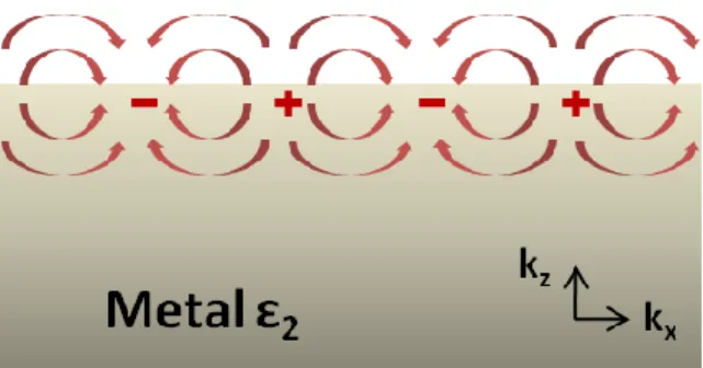
Fig. 1.1 Fig. 1.2: Fig. 1.3: Fig. 1.4: Fig. 1.5: Fig. 1.6:Illustration of the surface charges oscillations at the interface of metal and dielectric.
(a) The dispersion curve for a SP mode shows the momentum mismatch that must be overcome to couple light and SP modes. (b) The evanescent field of the SP modes at the interface of metal and dielectric. (adopted from [9])
Illustrations of (a) LSPR in the metallic nanosphere and (b) the metallic nanosphere in the constant electric field.
Examples of mode distribution affecting the LSPR frequency of a metal nanostructure. (a) Metal nanospheres imbedded in different dielectric media, (b) metal nanoshells of different thicknesses with bonding mode and (c) antibonding mode, (d) metal nanorods of different aspect ratios with field polarization parallel to the rod and (e) perpendicular to the rod. (adopted from [13])
LSPR wavelength (solid dot) and sensitivity (open dot) for gold (a) nanocylinders, (b) nanodisks, (c) Au/Au2S nanoshell and (d) hollow nanoshell. (adopted from [14])
(a) Measured extinction spectra and (b) SERS spectra for ring and ring dimer structures. The vertical dashed lines in (a) show the locations of the laser wavelengths and the Raman signal of benzenethiol. (adopted from [18]) 1 4 5 8 10 11
Chapter 2
Fig. 2.1: Fig. 2.2: Fig. 2.3:Triangular meshes for our simulation domain of the nanostructure dimer. Illustration of the fabrication process.
SEM images of (a) nanodisk dimers and (b) nanoring dimers with different gap sizes.
15 16 17
vii
Fig. 2.4: (a) Configuration and (b) photography of upright transmission spectroscopy. 19
Chapter 3
Fig. 3.1: Fig. 3.2: Fig. 3.3: Fig. 3.4: Fig. 3.5: Fig. 3.6: Fig. 3.7: Fig. 3.8: Fig. 3.9: Fig. 3.10: Fig. 3.11:Simulated extinction spectra of Au nanodisk dimers with different gap sizes in (a) longitudinal and (b) transverse polarizations.
The electric field distributions and flux lines of (a) longitudinal dipole mode, (b) longitudinal multipole mode, and (c) transverse dipole mode. Measured extinction spectra of Au nanodisk dimers with different gap sizes in (a) longitudinal and (b) transverse polarizations.
Simulated extinction spectra of Au nanoring dimers with different gap sizes in (a) longitudinal and (b) transverse polarizations.
The electric field distributions and flux lines of longitudinal (a) anti-bonding mode, (b) bonding mode, and (c) multipole bonding mode. Plot of the hybridization model for nanoring contributed from nanodisk and nanohole.
The electric field distributions and flux lines of transverse (a) anti-bonding mode, and (b) bonding mode.
Measured extinction spectra of Au nanoring dimers with different gap sizes in (a) none, (b) longitudinal and (c) transverse polarizations.
Simulated plot of longitudinal dipole mode wavelength shift as a function of gap size, which fits to an exponential-decay function. The inset is the illustration of the electromagnetic interaction between the nanodisks dimers in the longitudinal polarization.
Simulated electric field distributions of the longitudinal dipole mode with different gap sizes are shown in (a) top view at mid-height of the dimer and (b) side view along the dash line of inset. The position where y = 0 in (b) is the center of the gap shown as white area.
Simulated electric field intensities of the longitudinal dipole mode in the gap center with different gap sizes.
21 23 24 25 27 28 29 30 31 33 33
viii Fig. 3.12: Fig. 3.13: Fig. 3.14: Fig. 3.15: Fig. 3.16: Fig. 3.17:
Experimental results of the longitudinal dipole mode wavelength shift as a function of the gap size, which fits to an exponential-decay function.
Simulated plot of the wavelength shift as a function of the gap size for the longitudinal bonding mode, which fits to an exponential-decay function. Simulated electric field distributions of the longitudinal bonding mode with different gap sizes are shown in (a) top view at mid-height of the dimer and (b) side view along the dash line of inset. The position where y = 0 in (b) is the center of the gap shown as white area.
Simulated electric field distributions of the longitudinal anti-bonding mode with different gap sizes are shown in (a) top view at mid-height of the dimer and (b) side view along the dash line of inset. The position where y = 0 in (b) is the center of the gap shown as white area.
Simulated electric field intensities of the longitudinal bonding and anti-bonding modes in the gap center with different gap sizes.
Experimental results of the longitudinal bonding mode wavelength shift as a function of the gap size, which fits to an exponential-decay function.
34 35 36 37 38 38
Chapter 4
Fig. 4.1: Fig. 4.2: Fig. 4.3: Fig. 4.4: Fig. 4.5:Simulated peak wavelength as a function of the refractive index of surrounding medium for Au nanodisk dimers with different gap sizes in (a) longitudinal and (b) transverse polarizations.
Simulated bonding mode wavelength as a function of the refractive index of surrounding medium for Au nanoring dimers with different gap sizes in (a) longitudinal and (b) transverse polarizations.
Statistic of the simulated sensitivities of the longitudinal modes in Au nanoring and nanodisk dimers with different gap sizes.
Measured dipole mode wavelength of the Au nanodisk dimers with different gap sizes in air and alcohol in (a) longitudinal and (b) transverse polarizations.
Measured bonding mode wavelengths of the Au nanoring dimers with different gap sizes in air and alcohol in (a) longitudinal and (b) transverse polarizations. 41 42 43 44 45
ix
Fig. 4.6:
Fig. 4.7:
Statistic of measured wavelength shifts of the longitudinal modes in Au nanoring and nanodisk dimers with different gap sizes.
BSA protein molecule binding in the gap of a gold dimer. (adopted from [29]) 46 46
Appendix A
Fig. A.1: Fig. A.2:Refractive index and extinction coefficient spectra of ITO (adopted from [31])
(a) Simulated extinction spectrum and (b) longitudinal bonding mode wavelength shift with gap size variation of gold nanoring dimers on ITO glass substrate
50
1
Chapter 1 Introduction
1.1 Introduction to Surface Plasmon
Surface plasmons (SPs), are coherent electron oscillations that exist at the interface between metal and dielectric material where the real part of the dielectric function changes sign across the interface which shows in Fig.1.1. This characteristic phenomenon was first predicted in 1957 by R.H. Ritchie [1] and extensively studied in the following two decades by many scientists, the foremost of whom were Heinz Raether [2], E. Kretschmann, and A. Otto.
SP modes are confined around the surface of metals to form a highly near-field which has been wildly used in many spectro-applications, such as chemical or biological sensing, surface-enhanced Raman scattering (SERS) [3], and so on. In this chapter we would introduce the fundamental theory of SPs and describe the characteristics of SP modes on the surface of the metallic plane and nanoparticles by calculations, respectively[4].
Figure 1.1: Illustration of the surface charges oscillations at the interface of metal and dielectric.
2
1.1.1 Surface Plasmon Propagation
SPs would propagate at the interface between metals and dielectric materials by surface wave modes. Surface wave can propagate at the interface with TE and TM polarizations. The electric field direction is parallel in TE and perpendicular in TM to the interface which is z=0 in Fig.1.1. However, the electric field of TE modes should be continue in the metal-dielectric interface, so it’s impossible to induce charges to excite SPs. On the other hand for TM modes, the electric and magnetic field wave functions are as described in the following:
H =
E = (1-1)
The boundary conditions on the interface are
, ,
( : relative permittivity) (1-2) Considering of the symmetry of the surface wave (Ez,metal = -Ez,dielectric), the
relative permittivity relationship between the metal and the dielectric material should be
(1-3) The relative permittivity of metals under high frequency conditions derived by Drude’s model is
m p (1-4) ωp is the bulk plasma frequency. Take equation (1-4) into (1-3), we can get the surface
plasmon frequency
3
Then we use Maxwell equation:
to get ω ω ω ω (1-6) Finally take equations (1-6) into the boundary conditions (1-2), we can get the dispersion of SPs on the metallic-plane surface.
ω (1-7) The resulting momentum mismatch between light and SPs of the same frequency must be overcome if light is to be used to excite SPs as shown in Fig.1.2(a), and there are some techniques to achieve this condition. We can take advantage of prism coupling to enhance the momentum of the incident light [5][6] or involve scattering by nanostructures to excite the SPs locally [7][8].
Once light has generated an SP mode on a metallic plane, it will propagate but gradually decay because of absorption in the metal. When the intensity of the SP mode decays to 1/e, the propagation length is [2]
(1-8)
k”sp is the imaginary part of the wave vector of the SPs. Additionally, the intensity in the perpendicular direction to the interface of the metal and the dielectric material also exponentially decay as shown in Fig.1.2(b). The depth of which the intensity decayed to 1/e is
,
ω
(1-9)
4
other words, highly localized at SP resonance.
Figure 1.2 (a) The dispersion curve for a SP mode shows the momentum mismatch that must be overcome to couple light and SP modes. (b) The evanescent field of the SP modes at the interface of metal and dielectric. (adopted from [9])
1.1.2 Localized Surface Plasmon Resonance
As described in the last section, SP modes can be excited by nanostructrures in the sub-wavelength scale. Here we will concentrate on the metallic nanospheres for example by deriving some equations to describe the localized surface plasmon resonance behaviors.
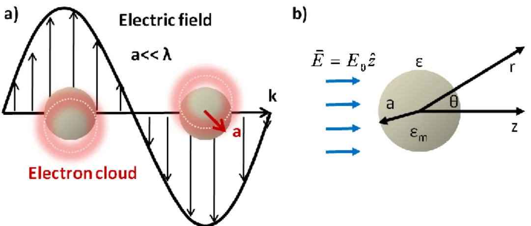
When the nanosphere size is much smaller than the wavelength scale of incident light, we can consider it in a constant electric field by using the quasi-static approximation. For a metallic nanosphere with radius a<<λ in a uniform electric field as shown in Fig.1.3 (b), the electric potentials in and out of the metallic sphere are
θ θ , (r<a)
θ θ θ , (r>a) (1-10)
5
Figure 1.3: Illustrations of (a) LSPR in the metallic nanosphere and (b) the metallic nanosphere in the constant electric field.
In order to solve Laplace’s equation , some boundary conditions should be achieved, which are
θ θ
(1-11)
Then we can get A and B which are
(1-12)
Take equation (1-12) back into (1-10), the electric potentials in and out of the metallic sphere become to
θ θ, (r<a)
θ θ θ , (r>a) (1-13)
What we focus is the electrical potential out of the sphere, , which can be also translated to
θ θ θ
,
6
Where p is dipole moment, and is polarizability.
The first term of is from the incident field, and the second term is induced by the ideal dipole. Here concerned of an ideal dipole ω at z=0 instead of the metallic sphere, which is surrounded by an incident plane wave with an electric field ω , the scattering electric field is
ω (1-15) We can calculate the extinction cross section from the equation (1-15):
θ
θ
,
λ (1-16)
As shown in the extinction cross section, there would be resonance when . And the localized surface plasmon resonance frequency can be obtained by Drude’s model:
ω ω
ω
, (in the air) (1-17)
If the shape of the nanoparticle is not a sphere, the localized surface plasmon resonance frequency would be varied with the geometry, which will be discussed in the next section.
7
1.2 LSPR Characteristics of Metal Nanostructures
For metal nanostructures with different geometries, the localized surface plasmon resonance frequency also can be obtained by modified Drude’s Model. For example of ellipsoidal shape, [10]
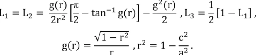
ω ω , (1-18) where Lj is the geometrical factor which will affect the value of the polarizability, .
The suitable coordinate system is the ellipsoidal coordinates (ξ,η,ζ) defined by ξ ξ ξ ,
η η η ,
ζ ζ ζ , (1-19) where a,b, and c are the lengths of the semi-major axes of the ellipsoid. Then the dipole moment, p, and thereby the polarizability, , can be identified as
where
with . One can show that L1 + L2 + L3 = 1 and L1
8
discuss another geometry, oblate spheroids, from this ellipsoid system for a special case where a = b, so
From r ~ 1 to r = 0, we can obtain different values of Ls then different LSPR mode frequencies for different geometries ranged from a disk to a sphere. Additionally, more geometries have been discussed in many papers. For a nanorod, L is directly related to the square of the nanorod aspect ratio [11] and to the metal shell thickness relative to the core size for the dielectric core-metal shell nanostructure [12]. For different LSPR mode frequencies of different geometries, the electron resonance behavior or the mode distribution would be different as shown in Fig.1.4, where even happens to high order or multipole oscillation modes in such nanostructures [13].
Figure 1.4: Examples of mode distribution affecting the LSPR frequency of a metal nanostructure. (a) Metal nanospheres imbedded in different dielectric media, (b) metal nanoshells of different thicknesses with bonding mode and (c) antibonding mode, (d) metal nanorods of different aspect ratios with field polarization parallel to the rod and (e) perpendicular to the rod. (adopted from [13])
9
1.3 LSPR Sensing
Whereas the above sections describe several fundamental spectroscopic relationships for different metal nanostructures, this section focuses on some biological and chemical sensing. Here we focus on two different sensing modes- wavelength-shift sensing and surface-enhanced Raman scattering sensing (SERS)-and their performances in different geometry systems.
1.3.1
Wavelength-Shift Sensing
The most common method for LSPR sensing is the wavelength-shift measurement, where the shift in the peak or the dip of the LSPR extinction curve is monitored as a function of refractive index variations in the dielectric environment. The relationship is described in the equation (1-20) derived from the equation (1-18):
λ , (1-20) where is the refractive index of the environment, and is the shape factor [12]. It is seen that the sensitivity of the LSPR to the medium is related to the shape factor varied with any metal geometry.
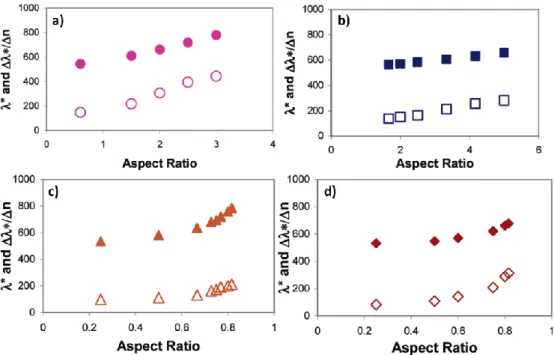
In 2005, Molly and Anne had taken some calculations for gold nanoparticles with some kinds of shape variations. Calculated LSPR peak wavelengths and sensitivities of peak wavelengths to the refractive index of the medium for gold nanoparticles with different aspect ratios defined as length to diameter in cylinders and diameter to height in disks are illustrated in Fig.1.5(a) and (b) [14]. The shape dependence of the LSPR sensitivities are also shown in Fig.1.5(c) and (d), where the aspect ratio is defined as the core radius to the shell thickness in nanoshells.
10
Figure 1.5: LSPR wavelength (solid dot) and sensitivity (open dot) for gold (a) nanocylinders, (b) nanodisks, (c) Au/Au2S nanoshell and (d) hollow nanoshell. (adopted from [14])
In 2007, the LSPR sensitivities for gold nanorings also had been investigated by
Elin M. Larsson et al. [15]. They found that the refractive index sensitivities of gold nanorings are substantially (>5 times) larger than those of nanodisks with similar diameters, where also concerned about substrate effects in their simulation.
1.3.2
Surface-Enhanced Raman Scattering Sensing
The second application in which the LSPR plays an important role is surface-enhanced Raman scattering (SERS) sensing. When the LSPR of the enhanced substrate properly matches with the Raman excitation and scattering wavelengths, it can boost the Raman cross section of molecules by many orders of magnitude even for a single molecule to be detected [16]. Here we describe some examples in which metal nanostructures are used as substrates for SERS sensing.
In 2003, N. Fe´ lidj et al. showed that tuning the maximum of the surface plasmon resonance of elongated gold nanoparticles to a wavelength, the position of
11
which is precisely midway between the exciting laser line and the Raman line, results in an optimization of the surface-enhanced Raman-scattering effect [17] .
In 2010, gold nanorings also served as substrates for SERS demonstrated by Mohamad G. and Kenneth B., in which the LSPR mode is highly tunable, better used as SERS substrate than nanodisks [18]. The Raman signal with ring dimer substrate is more enhanced than single ring substrate as shown in Fig.1.6.
Figure 1.6: (a) Measured extinction spectra and (b) SERS spectra for ring and ring dimer structures. The vertical dashed lines in (a) show the locations of the laser wavelengths and the Raman signal of benzenethiol. (adopted from [18])
1.4 Motivation and Thesis Organization
In recent years, it has been shown that the sensitivity of the LSPR frequency to the medium can be enhanced by tuning the geometry of the nanostructures such as nanoprisms [19], nanorods [11], or nanoshells [12]. Gold nanoring is another fine geometry with highly tunable and high LSPR sensitivity as described above. Additionally, the dependence of the nanoparticle surface plasmon resonance on the interaction between proximal nanoparticles has also been studied in detail [20]. The LSPR sensitivity can be more enhanced when metal nanoparticles come in close due to surface plasmon coupling [21]. However, most researchers focus on the wavelength-shift sensitivity in the particle dimer system only by simulation estimations. In this research, we expect not only to realize the gold nanodisk dimer in
12
experiment for LSPR wavelength-shift sensing but also further enhance the sensitivity in the nanoring dimer system.
The thesis is organized as following, in chapter 2, we introduce the simulation method, fabrication processes and measurement setup. In chapter 3, we study the optical properties of the SPR modes for both nanodisk and nanoring dimers with different gap sizes by simulations and experiments. In chapter 4, we further investigated the performance of wavelength-shift sensing application for both these nanostructure dimers by simulations and qualitatively by experiments. Finally, conclusion of research results and future work are discussed in chapter 5.
13
Chapter 2 Simulation Method, Fabrication
Process, and Measurement Setup
2.1 Introduction
In this chapter, we explained the fundamental theory of the numerical method to simulate the extinction spectrum and mode profiles of nanostructure dimers. To realize the structure, standard nano-fabrication processes for gold nanostructures including electron-beam lithography and thermal evaporation coating are introduced. For the fabricated devices characterization and sensing performance, we set up a upright transmission spectroscopy and its configuration is described.
2.2 Finite Element Method
In our simulation, Maxwell’s equations are solved by COMSOL Multiphysics (a commercial software) using finite element method (FEM) to find approximate solutions. Start from Maxwell’s equations, if we assume E-field and H-field are time harmonic modes, the vector wave equation for E-field can be derived as following:
Time harmonic H-field and E-field:
Maxwell’s equations: Vector wave equation of E-field:
14
where μr and r are in the tensor form, and n is refractive index. The time dependent
terms in electromagnetic field are eliminated in this wave equation because the assumption of time harmonic mode, thus obtained solution is stationary state. In order to solve this wave equation with appropriate boundary conditions, standard FEM proceeds in three steps.[22] First, the wave equation are identified as solutions of certain variational problems where the boundary conditions at the surface ∂V of the computational domain V have been incorporated as additional terms in the Lagrangian:
where n denotes the outward normal at the surface ∂V and the electric field has to satisfy the boundary condition n × E = 0 on ∂S. γe and U are known quantities which
are used to represent other types of boundary conditions such as scattering boundary conditions in our simulation.
The second step is discretization of the Lagrangian. The computational domain V is subdivided into a number of finite elements in three dimensions of triangular shape, as shown in Fig.2.1. Within each element, the electric field is expanded into a series of certain elementary functions with unknown coefficients.
In the final step, these expansions facilitate the transformation of the Lagrangian into a set of linear equations by Galerkin method [23] which is used to seek solutions by weighting the residual of the differential equation. These matrices can be solved by advanced linear algebra methods, either for obtaining eigenmodes of the system or to determine extinction cross sections of complex structures as well as transmittance and reflectance.
15
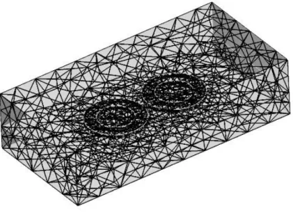
Figure 2.1: Triangular meshes for our simulation domain of the nanostructure dimer.
The refractive index of the substrate is taken to be 1.45, and the gold permittivity is modeled by Lorentz-Drude expression whose parameters are chosen to match the experimentally determined permittivity [24].
2.3 Fabrication Process
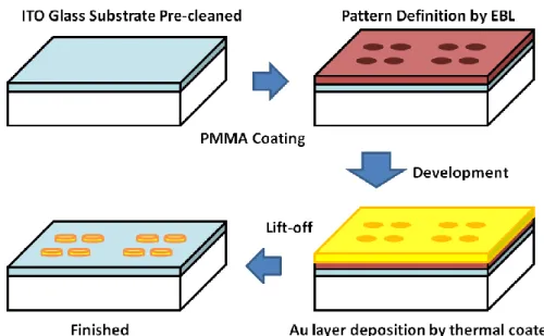
First, indium tin oxide (ITO) glass substrates are cleaned in acetone followed by isopropanol (IPA) for 20 min and dried in N2. Then these substrates are spin-coated
with 150 nm polymethyl methacrylate (PMMA) electron-sensitive resist followed by curing. The patterns for the nanodisk and nanoring dimer arrays are written on PMMA by using electron beam lithography system. During the expose step, pattern geometries can be controlled by choosing appropriate point and line dosage. The exposed PMMA becomes soluble and dissolves in e-beam resist developer (MIBK solution). Au layer with 50 nm of thickness is then deposited at a rate of 0.5 Å /s by thermal evaporation. Finally, the PMMA resist and the overlaying Au layer are removed by lift-off in acetone at room temperature. The illustration of overall fabrication process is shown in Fig.2.2.
16
Figure 2.2: Illustration of the fabrication process.
Following the procedure, we fabricated two dimensional 300 μm × 300 μm arrays of Au nanodisk and nanoring dimers with periods of 2 μm in the direction parallel to the dimer-axis and 1 μm in the perpendicular direction. The radius of nanodisk is ~190 nm; the inner and outer radiuses of nanoring are ~123 and ~252 nm, where the average radius is similar to the nanodisks. For the nanodisk dimers, the gap size varies as 28, 32, 75, 82, 209, and 313 nm; for the nanoring dimers, the gap size varies as 15, 47, 93, 145, 240, and 287 nm. The patterns are imaged by scanning electron microscope (SEM), as shown in Fig. 2.3.
17
Figure 2.3: SEM images of (a) nanodisk dimers and (b) nanoring dimers with different gap sizes.
18
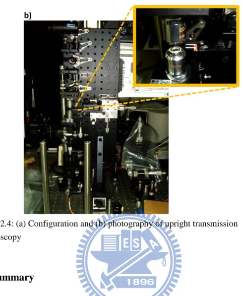
2.4 Measurement Setup
Fig. 2.4 shows the configuration and photography of upright transmission spectroscopy. Light from a halogen lamp is polarized by a polarizer, collimated and focused by a 20x objective lens on the sample at normal incidence. Alignment between the incident light and the sample can be adjusted by 3-axes stage where the sample is mounted. This adjustment can be monitoring by the projection of the pattern on a simple screen. Output signal is collected by another 20x objective lens and coupled into multimode fiber (MMF), which is finally analyzed by an optical spectrum analyzer (OSA). The extinction spectra as shown in the following are given by –log (P/P0), where P and P0 are the power of transmitted light with and without
passing through the patterns.
On the other hand, in order to investigate the optical sensing performance of devices, we change the environmental refractive index of nanodisk and nanoring dimers by immersing the fabricated device in alcohol (n~1.35), and obtaining their transmission spectra by the same upright transmission spectroscopy.
19
Figure 2.4: (a) Configuration and (b) photography of upright transmission spectroscopy
2.5 Summary
In this chapter, we introduced the fundamental theory of finite element method for our simulations. And we described the nano-fabrication processes for realizing the gold nanodisk and nanoring dimers, which are composed of e-beam lithography and thermal evaporation. Finally, we described the configuration of upright transmission spectroscopy and method to measure sensing performance of fabricated devices surrounding in different environments.
20
Chapter 3 Optical Properties of SPR Modes
for Gold Nanostructure Dimers
3.1 Introduction
In this chapter, the optical properties of SPR modes for gold nanostructure dimers with different gap sizes are investigated by simulations. The nanostructure dimers here we concern about are focused on slab-like geometries including nanodisk and nanoring. At first, we characterize the SPR modes from extinction spectrum and their related mode profiles in different polarizations, and then the mode wavelength-shift behavior and the field enhancement with varying gap size are further investigated. In addition, the corresponding optical properties are also realized in experiment.
3.2 SPR Mode Identification
3.2.1 Nanodisk Dimer
For the nanodisk dimer in simulation, the radius and the height are set to 200 nm and 50 nm, and the gap size varies from 350 down to 10 nm in simulation. The surrounding medium is assumed to be air. Incident plane waves of power 1 W and wavelength ranges from 400 to 1800 nm are employed to excite the nanodisk dimers. The case defined as longitudinal polarization is that the incident electric field is parallel to the dimer-axis, and the other defined as transverse polarization is that the electric field is perpendicular to the dimer-axis.
21
Fig.3.1 are given by –log (P/P0), where P and P0 are the transmitted power with and
without passing through the nanostructure dimers.
Figure 3.1: Simulated extinction spectra of Au nanodisk dimers with different gap sizes in (a) longitudinal and (b) transverse polarizations.
In longitudinal polarization, we can see a dominant mode red shift when the nanodisk dimers come in close. The electric field distribution of the dominant mode is depicted in Fig.3.2(a). We can see the electric field confined around the nanodisks in the dimer-axis and much concentrated in the gap. From the direction of the flux lines , it indicates the positive or negative charge distribution which is a dipolar SPR mode.
22
When the nanodisks come in close enough (< 50 nm), high-order mode would appear. The peak with wavelength ~900 nm in Fig.3.1(a) is a high-order and multipolar SPR mode as shown in Fig.3.2(b). On the other hand, the transverse mode doesn’t shift significantly with varying the gap size as shown in Fig.3.1(b) due to the electric field not concentrated in the gap. We can see the electric field distribution of this mode confined around the nanodisks but perpendicular to the dimer-axis as shown in Fig.3.2(c). The charge distribution is also a dipolar mode indicated from the flux lines.
23
Figure 3.2: The electric field distributions and flux lines of (a) longitudinal dipole mode, (b) longitudinal multipole mode, and (c) transverse dipole mode.
Figure 3.3 shows measured extinction spectra of the fabricated gold nanodisk dimers with similar size to the simulation. We also see a mode red-shift when the nanodisk dimers come in close in longitudinal polarization but no significantly shift in transverse polarization. Another high order mode also appears when the nanodisk dimers come in close enough (≦32 nm). All of these results are as the same as predicted in the simulation.
24
Figure 3.3: Measured extinction spectra of Au nanodisk dimers with different gap sizes in (a) longitudinal and (b) transverse polarizations.
3.2.2 Nanoring Dimer
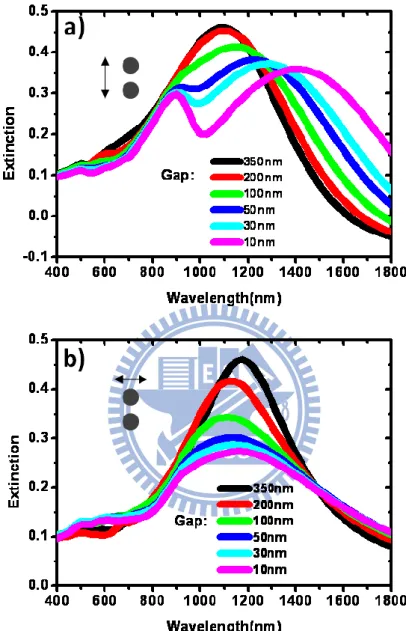
For the nanoring dimer in simulation, the outer and inner radiuses are set to 250 nm and 150 nm. The height is still 50 nm, and the gap size varies from 350 down to 10 nm. The surrounding medium is assumed to be air. Incident plane waves of power 1W and wavelength ranges from 400 to 2500 nm are employed to excite the nanoring dimer. The cases of longitudinal and transverse polarizations are defined as the same as mentioned for nanodisk dimer. The extinctions versus the wavelength in different polarizations as shown in Fig.3.4 are given by –log (P/P0) as mentioned in the last
25
Figure 3.4: Simulated extinction spectra of Au nanoring dimers with different gap sizes in (a) longitudinal and (b) transverse polarizations.
In longitudinal polarization, there are mainly two kind of modes as shown in Fig.3.4(a), and the electric field distributions of these two modes are shown in Fig.3.5. From the direction of the flux lines, they indicate the charge distributions which one is bonding mode in the near infrared range of wavelength and the other is anti-bonding mode in the visible range of wavelength. These two kind of modes have been well known since 2003 [25][26]. E. Prodan et al. presented a hybridization model for the plasmon response of complex nanostructures. Nanoring is one kind of complex
26
nanostructure which can be considered as a composition of nanodisk and nanohole, approximately 2D case of nanoshell which has been discussed in this reference paper. The nanohole and nanodisk plasmons are electromagnetic excitations that induce surface charges at inner and outer interfaces of the nanoring. Because of the finite thickness of the ring wall, the nanohole and nanodisk plasmon interact to each other. This interaction results in the splitting of the plasmon resonances into two new resonances: the lower energy bonding mode and the higher energy anti-bonding mode, as shown in Fig. 3.6. When the nanorings come in close, high-order mode would also appear. Figure 3.4(a) shows that a high-order mode is located in wavelength ~1200 nm of which the electric field distribution is multipole bonding mode, as shown in Fig. 3.5(c).
27
Figure 3.5: The electric field distributions and flux lines of longitudinal (a) anti-bonding mode, (b) bonding mode, and (c) multipole bonding mode.
28
Figure 3.6: Plot of the hybridization model for nanoring contributed from nanodisk and nanohole.
On the other hand for the transverse polarization, there are also appearing bonding and anti-bonding modes as shown in Fig. 3.4(b), the electric field distributions of which are shown in Fig. 3.7, but no significantly shift with varying gap size since the electric field is not concentrated in the gap.
29
Figure 3.7: The electric field distributions and flux lines of transverse (a) anti-bonding mode, and (b) bonding mode.
Figure 3.8 shows measured extinction spectra of the gold nanoring dimers with similar size and wall thickness to the simulation. There are also appearing two modes which one is anti-bonding mode in the visible range of wavelength and the other one is bonding mode in the near infrared range of wavelength, as shown in Fig.3.8(a). We can see bonding mode red-shift when the nanoring dimers come in close in longitudinal polarization but no significantly shift in transverse polarization. Another high order mode also appears in longitudinal polarization when the nanoring dimers come in close enough.
30
Figure 3.8: Measured extinction spectra of Au nanoring dimers with different gap sizes in (a) none, (b) longitudinal and (c) transverse polarizations.
31
3.3 Characteristics of Longitudinal SPR Modes with Varying Gap
Size
3.3.1 Nanodisk Dimer
In longitudinal polarization, the dipole mode would be much red shift when the nanodisk dimers come in close, as described in the last section. Figure 3.9 shows a simulated plot of the longitudinal dipole mode shift versus the gap size variation. The shift can be fit very nearly to an exponential decay function.
Figure 3.9: Simulated plot of longitudinal dipole mode wavelength shift as a function of gap size, which fits to an exponential-decay function. The inset is the illustration of the electromagnetic interaction between the nanodisks dimers in the longitudinal polarization.
The observed gap size dependent behavior of the longitude mode shift suggests a qualitative interpretation by a simple dipole-dipole interaction model which is well
32
explained by W. Rochberger et al. [20]. The electric field of the incident light would induce surface charges which feel repulsive force in the nanodisk at resonance. When another nanodisk is nearby, upon polarization additional force act on both nanodisks as sketch in the inset of Fig.3.9. If the driving field is parallel to the dimer-axis (longitudinal polarization), this effect results in a weakening of the repulsive forces for the surface charges. The positive charge of the left nanodisk in Fig.3.9 faces the corresponding negative charge of the right nanodisk. Due to the attractive forces between these two charge distributions of the different nanodisks, the repulsive forces within each nanodisk are weakened, leading to a correspondingly red shift of resonance wavelength.
In addition, the intensity of the electric field is more concentrated and enhanced with decreasing gap size as shown in Fig.3.10 and is nearly exponential decay with increasing gap size as shown in Fig.3.11. The field intensity in the gap of 10 nm is even 70 times stronger than that in the gap of 350 nm. The enhancement effect indicates that dimer system is critical for near-infrared sensitivity.
33
Figure 3.10: Simulated electric field distributions of the longitudinal dipole mode with different gap sizes are shown in (a) top view at mid-height of the dimer and (b) side view along the dash line of inset. The position where y = 0 in (b) is the center of the gap shown as white area.
Figure 3.11: Simulated electric field intensities of the longitudinal dipole mode in the gap center with different gap sizes.
Figure 3.12 shows a plot of the longitudinal mode shift versus the gap size variation for fabricated gold nanodisk dimers. The shift can also be fit very nearly to an exponential decay function, which is as the same as predicted in simulation.
34
Figure 3.12: Experimental results of the longitudinal dipole mode wavelength shift as a function of the gap size, which fits to an exponential-decay function.
3.3.2 Nanoring Dimer
Figure 3.13 shows a simulated plot of the longitudinal bonding mode shift versus the gap size variation. The shift can be fit very nearly to an exponential decay function, similar to the behavior of the longitudinal dipole mode for the nanodisk dimers where the charge distributions are almost the same, so it may be also attributed to the weakening repulsive force in the dimers modeled by the dipole-dipole interaction.
35
Figure 3.13: Simulated plot of the wavelength shift as a function of the gap size for the longitudinal bonding mode, which fits to an exponential-decay function.
Magda O. El-Shenawee also suggested this characteristic as a simple equivalent LC circuit oscillation [28]. In longitudinal polarization, the incident electric field in the gap is normal to the nanorings’ wall surface consistent with the charge signs in Fig.3.5(b). As the gap size decreases, the equivalent capacitance value increases. As a result, the resonance frequency proportional to 1/C decreases. This concept is consistent with the results observed in Fig. 3.4(a). In transverse polarization, the incident electric field in the gap is parallel to the nanorings’ wall surfaces. Accordingly, there is no effective capacitance caused by the gap, leading to insignificant effect of the gap size on the resonant wavelength observed in Fig. 3.4(b).
36
Fig. 3.14: Simulated electric field distributions of the longitudinal bonding mode with different gap sizes are shown in (a) top view at mid-height of the dimer and (b) side view along the dash line of inset. The position where y = 0 in (b) is the center of the gap shown as white area.
In addition, the intensity of the electric field is more concentrated and enhanced as gap size decreases for longitudinal bonding mode as shown in Fig. 3.14 and nearly exponential decay with increasing gap size as shown in Fig.3.16. The field intensity in the gap of 10 nm is about 57 times stronger than that in the gap of 350 nm and also stronger than that in the nanodisk dimers of the same gap size. This enhancement effect is similar to that for the nanodisk dimer because the bonding charge distribution of nanoring dimer is similar to the dipole mode of nanodisk dimer.
However, longitudinal anti-bonding mode doesn’t shift significantly with different gap sizes, as shown in Fig. 3.4(a). It attributed to the electric field intensity in the gap independent to gap size as shown in Fig. 3.15 & 3.16, maybe due to the anti-bonding charge distribution.
37
Figure 3.15: Simulated electric field distributions of the longitudinal anti-bonding mode with different gap sizes are shown in (a) top view at mid-height of the dimer and (b) side view along the dash line of inset. The position where y = 0 in (b) is the center of the gap shown as white area.
38
Figure 3.16: Simulated electric field intensities of the longitudinal bonding and anti-bonding modes in the gap center with different gap sizes.
Figure 3.17 shows a plot of the longitudinal bonding mode shift versus the gap size variation for fabricated gold nanoring dimers. The shift can also be fit very nearly to an exponential decay function, which is as the same as predicted in simulation.
Figure 3.17: Experimental results of the longitudinal bonding mode wavelength shift as a function of the gap size, which fits to an exponential-decay function.
39
3.4 Summary
In this chapter, we identified and characterized the properties of SPR modes with gap size variation in nanodisk and nanoring dimers by simulations then realized by experiments. For nanodisk dimers, there is a dipole mode in each polarization and appearing a high-order mode in longitudinal polarization when the nanodisk dimers come in close. On the other hand, for nanorings dimers, there are anti-bonding mode and bonding mode in each polarization and also appearing a high-order mode in longitudinal polarization when the nanoring dimers come in close, which can be characterized by hybridization model. We further find that the wavelengths of longitudinal dipole mode in nanodisk dimers and longitudinal bonding mode in nanoring dimers are red-shift as an exponential function with decreasing gap size. Moreover, the electric field intensities are more enhanced with decreasing gap size and also decay as an exponential function with increasing gap size. And the electric field intensity in the gap for nanoring dimer is stronger than nanodisk dimer, which indicates better sensing ability in nanoring dimer system.
40
Chapter 4 Sensing Application
4.1 Introduction
In this chapter, we change the environmental refractive index of the nanostructure dimers by simulation to investigate the optical sensing performance. In addition, we immerse the fabricated device in alcohol to detect the wavelength shift with varying the refractive index in experiment.
4.2 Wavelength-Shift Sensing Performance
Similar to isolated nanoparticles [14][27], there is a red shift in the plasmon resonance of the two-particle system as the medium refractive index is increased since the Coulombic restoring force acting on the polarized charges is reduced in the higher refractive index medium[21]. Figure 4.1 shows a plot of the simulated dipole mode wavelength of the nanodisk dimers as a function of the refractive index of surrounding medium. As the gap size is decreased from 350 nm to 10 nm, the sensitivity which is the wavelength shift per refractive index unit (RIU) in longitudinal polarization increases from 367 nm/RIU to 901 nm/RIU, which is much higher than the value of ~400 nm/RIU in transverse polarization where the sensitivity can be not enhanced with decreasing gap size. The sensitivity of 901 nm/RIU in longitudinal polarization is also higher than the value of 434 nm/RIU reported before for smaller gold nanodisk dimers calculated by discrete dipole approximation (DDA) [21], and it can be much higher by optimizing the aspect ratio [14].
41
Figure 4.1: Simulated peak wavelength as a function of the refractive index of surrounding medium for Au nanodisk dimers with different gap sizes in (a) longitudinal and (b) transverse polarizations.
For nanoring dimers, the simulated bonding mode wavelength as a function of the medium refractive index for different values is shown in Fig. 4.2. As the gap size is decreased from 350 nm down to 10 nm, the sensitivity of the longitudinal bonding mode increases from 658 nm/RIU to 1076 nm/RIU which is much higher than the value of ~720 nm/RIU in transverse where the sensitivity can be not enhanced with decreasing gap size. The sensitivity of 1076 nm/RIU can be much higher by
42
optimizing the ring wall thickness.[28]
Figure 4.2: Simulated bonding mode wavelength as a function of the refractive index of surrounding medium for Au nanoring dimers with different gap sizes in (a)
longitudinal and (b) transverse polarizations.
From the statistic of the simulated sensitivities for both nanodisk and nanoring dimers as shown in Fig. 4.3, the sensitivities are increasing with decreasing gap size due to more enhanced intensity of the electric field concentrated in the gap. Moreover, the sensitivity is much higher for the nanoring dimers because the electric field is not only stronger in the gap but also distributed on more surfaces of inner ring leading to
43
more interactions with mediums.
Figure 4.3: Statistic of the simulated sensitivities of the longitudinal modes in Au nanoring and nanodisk dimers with different gap sizes.
In experiment, we change the environmental refractive index of the nanostructure dimers by immersing the fabricated device in alcohol of which the refractive index is ~1.35. Figure 4.4 shows a plot of the simulated dipole mode wavelength of the nanodisk dimer in air and alcohol. As the gap size is decreased from 313 nm to 28 nm, the wavelength shift in longitudinal polarization increases from 431 nm/RIU to 531 nm/RIU, which is higher than the value of ~401 nm/RIU in transverse polarization where the sensitivity can be not enhanced with decreasing gap size.
44
Figure 4.4: Measured dipole mode wavelength of the Au nanodisk dimers with different gap sizes in air and alcohol in (a) longitudinal and (b) transverse polarizations.
For nanoring dimers, the measured bonding mode wavelength as a function of the refractive index of surrounding medium is shown in Fig. 4.5. As the gap size is decreased from 287 nm to 47 nm, the sensitivity of the longitudinal bonding mode increases from 620 nm/RIU to 663 nm/RIU which is higher than the value of ~611 nm/RIU in transverse polarization where the sensitivity can be not enhanced with decreasing gap size.
45
Figure 4.5: Measured bonding mode wavelengths of the Au nanoring dimers with different gap sizes in air and alcohol in (a) longitudinal and (b) transverse
polarizations.
From the statistic of the measured wavelength shifts for both nanodisk and nanoring dimers as shown in Fig.4.6, the wavelength shifts in different environments are increased with decreasing gap size, which agrees to the trends predicted in simulation. Moreover, the wavelength shifts is higher for the nanoring dimers, which is also in accordance with the simulation results.
46
weaker in experiment. In bulk liquid sensing, it’s difficult for liquid to be fully filled in the small-size gap due to the surface tension. Therefore, the electric field enhanced in the gap can not respond to the wavelength shift with varying environments (sensitivity). Nevertheless, it still has potentials on wavelength-shift sensing, such as bio-medicine and bio-chemical nanosensing. The nanostructure dimers can provide a higher sensitivity to local perturbations like molecule binding. [29]
Figure 4.6: Statistic of measured wavelength shifts of the longitudinal modes in Au nanoring and nanodisk dimers with different gap sizes.
Figure 4.7: BSA protein molecule binding in the gap of a gold dimer. (adopted from [29])
47
4.3 Summary
In this chapter, we proposed the wavelength-shift index sensing performance for the nanodisk and nanoring dimers by simulation. The simulated sensitivity for the nanodisk dimer is up to 901 nm/RIU and even improved to 1076 nm/RIU for nanoring dimer with gap size of 10 nm because the bonding mode of nanoring dimer is a stronger dipole coupling leading to more enhanced electric field in the gap. However, this enhancement is not obvious in experiment because the liquid is difficult to be fully filled in the gap of nanostructure dimer. Nevertheless, we believe that it still has potentials for nanosensing applications such as protein, DNA or toxic chemical molecule detections.
48
Chapter 5 Conclusion and Future Work
5.1 Conclusion
In this thesis, optical properties of SPR modes in nanodisk and nanoring dimers are investigated by simulation and experiment. At first, we identified these SPR modes are dipole, multipole modes in nanodisk dimer, and bonding, anti-bonding, multipole bonding modes in nanoring dimer for different polarizations from the charge distributions by simulation. In the further investigation, for longitudinal polarization, wavelength-shift behavior as a exponential decay function with increasing gap size is observed in both simulation and experiment. For these dimer systems, the electric field in the gap can be also enhanced with decreasing gap size. Moreover, the electric field is stronger in nanoring dimer. Base on these optical properties, a wavelength-shift index sensitivity obtained by simulation is up to 901 nm/RIU in nanodisk dimer and further improved to 1076 nm/RIU in nanoring dimer. These results indicate that it’s critical for optical sensing application. In our experiment, the wavelength shifts in different environments also increase with decreasing gap size but not obviously for such a bulk liquid sensing. It attributed to the liquid not fully filled in the gap due to the surface tension. We consider that it’s more suitable for nanosensing applications.
49
5.2 Future Work
In addition to sensing bulk refractive index changes, the nanostructure dimer is more suitable for nanosensing especially for bio-sensing applications. It’s more likely to enable high sensitivity to local perturbations such as small molecules binding on the metal surface. To realize nanosensing research, the gold nanostructure dimer can be bound with some kinds of protein to detect the wavelength shift. Moreover, this dimer system can trap and detect other kinds of molecules or particles by optical force induced from the enhanced electric field in the gap.[30]
50
Appendix A: Influence of Dielectric Properties
of ITO Glass Substrate upon SPR Spectrum
In chapter 3, we have discussed the SPR mode properties generally for gold nanostructure dimers on glass substrate of which the refractive index is nearly a constant (n=1.45). However, in our experiment, there have to be a conductive layer such as ITO film underlaid to facilitate the pattern definition by e-beam lithography. The optical properties of ITO film are wavelength dependent and absorptive for infrared spectrum. The refractive index and extinction coefficient spectra are shown in figure A.1.[31]
Figure A.2 shows simulated extinction spectrum of gold nanoring dimers on ITO glass substrate in longitudinal polarization. We find that anti-bonding mode is red-shift and bonding mode is blue-shift comparing to the simulation results for glass substrate (Fig. 3.4), which almost match to the experimental results (Fig. 3.8). In addition, the line widths of peaks are narrower for ITO substrate. These characteristics are all attributed to the refractive index dispersion and absorption dependent on wavelengths of ITO leading to affect the SPR peak structure [32].
51
[31])
Figure A.2: (a) Simulated extinction spectrum and (b) longitudinal bonding mode wavelength shift with gap size variation of gold nanoring dimers on ITO glass substrate
52
References
[1] R. H. Ritchie, “Plasma Losses by Fast Electrons in Thin Films,” Phys. Rev. Lett,
106, 874-881 (1957).
[2] H. Raether, “Surface Plasmons,” Springer, New York, (1988).
[3] M. Moskovits, “Surface-enhanced spectroscopy,” Rev. Mod. Phys. 57, 783, (1985)
[4] 吳民耀, 劉威志, “表面電漿子理論與模擬,” 物理雙月刊, 二十八卷二期, (2006)
[5] Kretschmann, E. & Raether, H. “Radiative decay of nonradiative surface plasmons excited by light,” Z.Naturforsch. A 23, 2135–2136 (1968).
[6] Otto, A. “Exitation of nonradiative surface plasma waves in silver by the method of frustrated total reflection,” Z. Phys. 216, 398 (1968).
[7] Hecht, B., Bielefeldt, H., Novotny, L., Inouye, Y. & Pohl, D. W. “Local
excitation, scattering, and interference of surface plasmons,” Phys. Rev. Lett. 77, 1889–1892 (1996).
[8] Ditlbacher, H. et al. “Fluorescence imaging of surface plasmon fields,” Appl.
Phys. Lett. 80, 404–406 (2002).
[9] William L. Barnes, Alain Dereux, Thomas W. Ebbesen, “Surface plasmon subwavelength optics” Nature, 424, 824 (2003)
[10] G. Mukhopadhyay, “Dielectric Response Of Nanoparticles”.
[11] Lee, K.-S., El-Sayed, M. A. “Gold and Silver Nanoparticles in Sensing and Imaging: Sensitivity of Plasmon Response to Size, Shape, and Metal Composition” J. Phys. Chem. B, 110, 19220 (2006).
[12] Jain, P. K., El-Sayed, M. A. “Surface Plasmon Resonance Sensitivity of Metal Nanostructures: Physical Basis and Universal Scaling in Metal Nanoshells” J.
53
Phys. Chem. C, 111, 17451–17454 (2007).
[13] Feng Wang, Y. Ron Shen, “General Properties of Local Plasmons in Metal Nanostructures,” Phys. Rev. Lett. 97, 206806 (2006)
[14] Molly M. Miller, Anne A. Lazarides, “Sensitivity of Metal Nanoparticle Surface Plasmon Resonance to the Dielectric Environment,” J. Phys. Chem. B, 109, 21556 (2005)
[15] Elin M. Larsson, Joan Alegret, Mikael Kall, Duncan S. Sutherland, “Sensing Characteristics of NIR Localized Surface Plasmon Resonances in Gold Nanorings for Application as Ultrasensitive Biosensors,” Nano Lett., 7, 1256 (2007)
[16] J. A. Dieringer, R. B. Lettan II, K. A. Scheidt, R. P. Van Duyne, “A Frequency Domain Existence Proof of Single-Molecule Surface-Enhanced Raman
Spectroscopy” J. Am. Chem. Soc. 129, 16249 (2007).
[17] N. Fe´ lidj, J. Aubard, G. Le´ vi, J. R. Krenn, A. Hohenau, G. Schider, A. Leitner, and F. R. Aussenegg, “Optimized surface-enhanced Raman scattering on gold nanoparticle arrays,” Appl. Phys. Lett. 82, 3095 (2003)
[18] Mohamad G. Banaee and Kenneth B. Crozier, “Gold nanorings as substrates for surface-enhanced Raman scattering,” Opt. Lett. 35, 760 (2010)
[19] Haes, A. J.; Van Duyne, R. P. “A Nanoscale Optical Biosensor: Sensitivity and Selectivity of an Approach Based on the Localized Surface Plasmon Resonance Spectroscopy of Triangular Silver Nanoparticles,” J. Am. Chem. Soc. 124, 10596 (2002)
[20] Rechberger, W.; Hohenau, A.; Leitner, A.; Krenn, J. R.; Lamprecht, B.;
Aussenegg, F. R. “Optical properties of two interacting gold nanoparticles” Opt.
Commun., 220, 137–141 (2003)
[21] Prashant K. Jain, Mostafa A. El-Sayed, “Noble Metal Nanoparticle Pairs: Effect of Medium for Enhanced Nanosensing” Nano Lett. 8, 4347 (2008)
54
[22] K. Buscha, G. von Freymann, S. Linden, S.F. Mingaleev, L. Tkeshelashvili, M. Wegener, “Periodic nanostructures for photonics” Phy. Rep.444, 101
[23] Jianming Jin, “The Finite Element Method in Electromagnetics” Wiley, New York, (1993)
[24] Aleksandar D. Rakic´, Aleksandra B. Djurisˇ ic´, Jovan M. Elazar, Marian L. Majewski, “Optical properties of metallic films for vertical-cavity optoelectronic devices” Appl. Opt. 37, 5271 (1998)
[25] J. Aizpurua, P. Hanarp, D. S. Sutherland, M. Ka¨ ll, Garnett W. Bryant, F. J. Garcı´a de Abajo, “Optical Properties of Gold Nanorings” Phy. Rev. Lett. 90, 057401 (2003)
[26] E. Prodan, C. Radloff, N. J. Halas, P. Nordlander, “A Hybridization Model for the Plasmon Response of Complex Nanostructures” Science, 302, 419 (2003)
[27] Magda O. El-Shenawee, “Polarization Dependence of Plasmonic Nanotoroid Dimer Antenna”, IEEE ANTENNAS AND WIRELESS PROPAGATION
LETTERS, 9, 463 (2010)
[28] Chia-Yang Tsai, Shao-Ping Lu, Jyun-Wei Lin, Po-Tsung Lee, “High sensitivity plasmonic index sensor using slablike gold nanoring arrays”, Appl. Phys. Lett.,
98, 153108 (2011)
[29] Srdjan S. Ac´imovic´, Mark P. Kreuzer, María U. González, Romain Quidant, “Plasmon Near-Field Coupling in Metal Dimers as a Step toward
Single-Molecule Sensing”, Nano Lett, 5, 1231 (2009)
[30] Weihua Zhang, Lina Huang, Christian Santschi, Olivier J. F. Martin, “Trapping and Sensing 10 nm Metal Nanoparticles Using Plasmonic Dipole Antennas”,
Nano Lett, 10, 1006 (2010)
[31] R.A. Synowicki, “Spectroscopic Ellipsometry Characterization of Indium Tin Oxide Film Microstructure and Optical Constants”, Thin Solid Films, 313, 394,(1998)
55
substrate upon plasmon resonance spectrum of supported Ag nanoparticles”,
56
Vita
Jyun-Wei Lin was born on 27, November, 1986 in
Taipei, Taiwan. He received the B. S. degree from the Department of Material Science and Engineering, National Tsing Hua University (NTHU), Hsinchu, Taiwan, in 2009 and the M. S. degree from the Institute of Electro-Optical
Engineering, National Chiao Tung University (NCTU), Hsinchu, Taiwan, in 2010. His research was focused on plasmonic nanostructures and 1D photonic crystal reflectors.
Publications:
[1] Chia-Yang Tsai, Shao-Ping Lu, Jyun-Wei Lin, Po-Tsung Lee, “High sensitivity plasmonic index sensor using slablike gold nanoring arrays”, Appl. Phys. Lett.,
98, 153108 (2011)
(Selected for Virtual Journal of Nanoscale Science & Technology, Vol. 23, issue16, April.13, 2011)
[2] Jyun-Wei Lin, Chia-Yang Tsai, Po-Tsung Lee, “One Dimensional Composite
Gradual Photonic Crystal With Broadband Omni-Directional Reflection”, OPT, OPT5-O-031(2010)