New Low-Leakage Power-Rail ESD Clamp Circuit
in a 65-nm Low-Voltage CMOS Process
Ming-Dou Ker, Fellow, IEEE, and Po-Yen Chiu, Student Member, IEEE
Abstract—A new low-leakage power-rail electrostatic discharge
(ESD) clamp circuit designed with consideration of the gate leak-age issue has been proposed and verified in a 65-nm low-voltleak-age CMOS process. Consisting of the new low-leakage ESD-detection circuit and the ESD clamp device of a substrate-triggered sili-con-controlled rectifier, the new proposed power-rail ESD clamp circuit realized with only thin-oxide (1-V) devices has a very low leakage current of only 116 nA at room temperature (25◦C) under the power-supply voltage of 1 V. Moreover, the new proposed power-rail ESD clamp circuit can achieve ESD robustness of over 8 kV, 800 V, and over 2 kV in human-body-model, machine-model, and charged-device-model ESD tests, respectively.
Index Terms—Electrostatic discharge (ESD), gate leakage,
power-rail ESD clamp circuit, substrate-triggered silicon-controlled rectifier (STSCR).
I. INTRODUCTION
T
HE gate-tunneling current has been a serious leakage issue in nanoscale CMOS technologies when the gate oxide becomes thinner. With a large gate-tunneling current, CMOS integrated circuits (ICs) may not work correctly because the gate voltage could be discharged through the leaky gate oxide. Therefore, the gate leakage issue must be considered during the circuit design phase of ICs before fabrication in nanoscale CMOS processes [1], [2]. To effectively protect the internal circuits against electrostatic discharge (ESD) damages, on-chip ESD protection circuits have to be built in the IC chip [3]–[6]. Unfortunately, on-chip ESD protection circuits in nanoscale CMOS processes also suffer the gate leakage issue. The traditional ESD protection designs may work incorrectly due to the gate leakage current. To solve this issue, a new design to reduce the leakage current of on-chip ESD protection circuits has been requested by the IC industry. Although the gate leakage issue can be mitigated by using a high-k dielectric with a metal gate [7], [8], high-k dielectric materials are still notManuscript received May 14, 2009; revised September 7, 2009, November 27, 2009, and March 31, 2010; accepted August 4, 2010. Date of publication August 16, 2010; date of current version September 2, 2011. This work was supported in part by the National Science Council, Taiwan, under Contract NSC 98-2221-E-009-113-MY2, by the Ministry of Economic Affairs, Taiwan, under Grant 98-EC-17-A-01-S1-104, by the National Chiao Tung University and Ministry of Education, Taiwan, through the “Aim for the Top University Plan,” and by the Faraday Technology Corporation, Taiwan.
M.-D. Ker is with the Nanoelectronics and Gigascale Systems Laboratory Institute of Electronics, National Chiao Tung University, Hsinchu 300, Taiwan, and also with the Department of Electronic Engineering, I-Shou University, Kaohsiung County 84001, Taiwan (e-mail: [email protected]).
P.-Y. Chiu is with the Nanoelectronics and Gigascale Systems Laboratory Institute of Electronics, National Chiao Tung University, Hsinchu 300, Taiwan.
Digital Object Identifier 10.1109/TDMR.2010.2066976
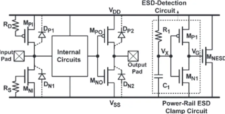
Fig. 1. Typical whole-chip ESD protection scheme in CMOS ICs.
supported in most foundry CMOS processes in the 45–90-nm technology nodes.
In order to protect the internal circuits from ESD stresses, on-chip ESD protection circuits must be applied to all input/output (I/O) and power (VDD/VSS) pads. The concept of the
whole-chip ESD protection design for CMOS ICs is illustrated in Fig. 1. The power-rail ESD clamp circuit plays a vital role in the whole-chip ESD protection design because it can effectively discharge the ESD current under ESD stresses [9]. With the turn-on efficient power-rail ESD clamp circuit between the VDD
and VSS power lines, the ESD protection devices/circuits at
the I/O pads can be realized with small dimensions to achieve high ESD robustness [10]. In the traditional designs, the power-rail ESD clamp circuits were often realized with an RC-based ESD-detection circuit and a main ESD clamp device (MNESD
shown in Fig. 1) with a large dimension to achieve high ESD robustness.
For the sake of reducing the layout area, the capacitor (C1in
Fig. 1) in the traditional RC-based ESD-detection circuit was often realized by a MOS capacitor because the MOS capacitor has the largest capacitance per unit area in the baseline CMOS processes. However, the gate-oxide thickness becomes thinner and thinner in the nanoscale CMOS technology, which makes the gate-tunneling leakage more significant and can no longer be ignored. The gate leakage issue has been studied, and the mechanism of the gate-direct-tunneling current has been modeled for a circuit simulation [11], [12]. The physically based model and semiempirical equations can help to address the impacts of the gate leakage current on the device or circuit performance. With the increased gate leakage current of MOS transistors in the nanoscale CMOS processes, the power-rail ESD clamp circuit with a large MOS capacitor in the traditional
RC-based ESD-detection circuit was reported to suffer a huge
leakage current and undesired static power consumption [13]. To solve this problem, some designs to reduce the leakage
current of the power-rail ESD clamp circuit has been re-ported [13]–[15]. Since ICs with lower power consumption are preferred, any redundant leakage current must be eliminated. Hence, the gate leakage issue in the power-rail ESD clamp circuit fabricated in nanoscale CMOS processes should be solved.
In this paper, a new low-leakage power-rail ESD clamp circuit realized by only thin-oxide (low-voltage) devices is proposed and verified in a 65-nm CMOS process [16]. The impact of the gate leakage current on a traditional power-rail ESD clamp circuit in nanoscale CMOS processes is discussed in Section II. In Section III, the operation of the new proposed low-leakage power-rail ESD clamp circuit is described, and the simulated results are presented. Finally, the experimental verifications in a silicon chip, including the leakage current and ESD robustness, are presented in Section IV.
II. IMPACTS OFGATELEAKAGECURRENT ON
TRADITIONALPOWER-RAILESD CLAMPCIRCUIT
To efficiently turn on the power-rail ESD clamp circuit during ESD stresses and to completely keep it off under normal circuit operating conditions, the RC time constant of the ESD-detection circuit is often designed around 0.1–1 μs. Under the ESD-stress condition, the ESD voltage has a rise time on the order of nanoseconds. The voltage level of VX in Fig. 1 is
increased much slower than the voltage level at the VDDpower
line when the ESD stress is conducted across the VDDand VSS
power lines. Due to the RC delay, the PMOS MP 1in the
ESD-detection circuit will be turned on to boost the voltage at the node VG to turn MNESD on. The turned-on MNESD, which
provides a low-impedance path between VDD and VSS, can
discharge the ESD current from VDDto VSS. Under the normal
power-on transition, the VDD power-on voltage waveform has
a rise time on the order of milliseconds. With such a slow rise time of the VDD power-on transition, the voltage at VX
in the ESD-transient-detection circuit can follow up the VDD
voltage in time to keep MP 1 off. Moreover, MN 1is turned on
to keep VG at a voltage level of 0 V. Consequently, MNESD
is completely kept off to avoid the leakage when the IC is under normal circuit operating conditions after the power-on transition.
In nanoscale CMOS processes, the serious gate-tunneling phenomenon leads to a large leakage current through the MOS capacitor in the ESD-detection circuit. With a large gate leakage current in the MOS capacitor, the voltage at VX in Fig. 1
cannot be fully charged to VDD after the power-on transition,
as illustrated in Fig. 2. Therefore, the PMOS MP 1 in the
ESD-detection circuit cannot be fully turned off, which causes another leakage path through the inverter in the ESD-detection circuit. Consequently, in the traditional power-rail ESD clamp circuit shown in Fig. 1, the gate voltage of MNESD cannot be
fully biased to VSS. The partially turned-on MNESD (which
is designed with a large device dimension) will conduct more leakage current from VDDto VSSunder normal circuit operating
conditions.
Some previous works have addressed the impact of the gate leakage on the power-rail ESD clamp circuit, and several
Fig. 2. Gate leakage issue in the traditional ESD-detection circuit after VDD
power-on transition.
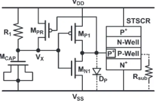
Fig. 3. Power-rail ESD clamp circuit with the PMOS restorer (MPR) [10]. designs to reduce the leakage current have been reported [13]–[15]. As shown in Fig. 3, an additional PMOS restorer (MPR) in the ESD-detection circuit has been proposed to pull
high the voltage level at VX. As a result, MP 2 is effectively
turned off under normal circuit operating conditions, and the leakage current is reduced [13]. With a similar idea, another de-sign using the latch technique to reduce the requested capacitor size in the ESD-detection circuit, which, in turn, decreases the leakage current of the power-rail ESD clamp circuit, has also been reported [14]. Recently, a design using the stacked MOS capacitors to reduce the voltage across each MOS capacitor and adjusting the bias points of the devices in the ESD-detection circuit has been reported to decrease the gate leakage current of a MOS capacitor [15]. By controlling the voltage across the gate of the devices in the ESD-detection circuit, the leakage current of the power-rail ESD clamp circuit can be decreased. However, with the stacked MOS capacitors, the effective capacitance is reduced, so the trigger time of the ESD-detection circuit under an ESD-stress condition is decreased. To achieve an identical
RC time constant in the ESD-detection circuit, more layout
area is required to increase the effective capacitance of the stacked MOS capacitors.
Another design, which utilizes the current amplification tech-nique in an ESD-detection circuit, is promising to reduce the requested capacitor size which can, in turn, reduce the leakage current of the power-rail ESD clamp circuit [17]. With the current amplification technique, the effective capacitance of a MOS capacitor is multiplied. Thus, the required area to realize the MOS capacitor can be reduced, and the leakage current through the MOS capacitor can also be reduced. Such previous
Fig. 4. New proposed low-leakage power-rail ESD clamp circuit.
works can reduce the leakage current of the power-rail clamp circuit or mitigate the impact of a leaky MOS capacitor in nanoscale CMOS processes. However, the voltage across the MOS capacitor in the ESD-detection circuit is still at a high voltage level under normal circuit operating conditions. The gate leakage current through the MOS capacitor still exists in those previous designs.
III. NEWPROPOSEDLOW-LEAKAGEPOWER-RAIL
ESD CLAMPCIRCUIT
In the BSIM4 MOSFET model [18], the gate-direct-tunneling current has been modeled. The equations of the gate-direct-tunneling current indicate that the leakage current through the MOS capacitor can be reduced by reducing the voltage across it. Based on this concept, the MOS capacitor in the new ESD-detection circuit is designed without a voltage drop across it under normal circuit operating conditions. Under an ESD-stress condition, the new ESD-detection circuit is designed to provide the trigger current to turn on the ESD clamp device.
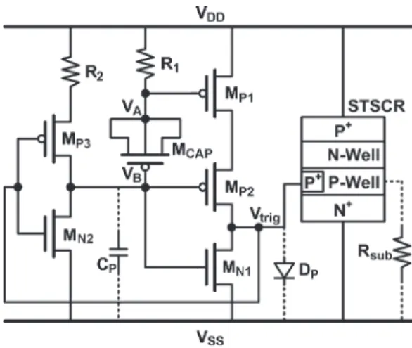
The new proposed power-rail ESD clamp circuit to overcome the gate leakage issue is shown in Fig. 4, which consists of the new ESD-detection circuit and the ESD clamp device. In the new ESD-detection circuit, the RC-based ESD-detection cir-cuit and the feedback-control inverter are combined together, and the MOS capacitor (MCAP) is connected between the VA
and VBnodes. Because MCAPis not directly connected to VSS,
no direct leakage path is conducted through the MOS capacitor to the ground under normal circuit operating conditions. The selected device dimensions in the new ESD-detection circuit in this paper are listed in Table I. Without the thin gate oxide in the p-n-p-n structure of an SCR, the SCR is free to the gate leakage issue as compared with a large MOSFET. Therefore, the substrate-triggered SCR (STSCR) is used as the main ESD clamp device in the new proposed low-leakage power-rail ESD clamp circuit, as shown in Fig. 4. Furthermore, the SCR has been proven to have the highest ESD robustness and the smallest device size [19]. The STSCR used in this paper is shown in Fig. 5, wherein the layout of the STSCR is drawn with a length of 7.8 μm and a width of 60 μm.
TABLE I
DEVICEDIMENSIONSSELECTED IN THENEW
ESD-DETECTIONCIRCUIT
Fig. 5. Device cross-sectional view of STSCR.
A. Operation Under Normal Circuit Operating Conditions
With a slow rise time of the normal power-on transition, the voltage levels at VAwill be able to follow up the VDDvoltage
waveform in time to keep MP 1 off. Moreover, the parasitic
p-substrate resistor (Rsub) and p-well/n+ diode (DP) in the
STSCR structure, which are inherently formed at the trigger node (Vtrig) of the STSCR, can pull the Vtrigto VSS. The MP 3
would also be turned on to drive the node VBto VDDduring the
power-on transition. With the node VB voltage of VDD, MP 2
can be fully turned off. In addition, MN 1is turned on because
its gate terminal is connected to VB. Through the feedback
path, MN 2can be turned off, and MP 3can be kept on to fully
charge the voltage at VA and VB to VDD. Consequently, there
is no voltage drop across MCAP, and no circuit leakage path
exists in the new ESD-detection circuit. Without a voltage drop across MCAPunder normal circuit operating conditions, MCAP
can be realized with a large device size without suffering the leakage current. Since VA and VB are charged to VDD, MP 1
and MP 2 can be fully turned off during the normal
power-on transitipower-on; therefore, no trigger current is injected into the STSCR. As a result, the STSCR can be kept off under normal circuit operating conditions. Therefore, the inherent Rsuband
DP in the STSCR enhance the immunity of the new proposed
design from being mistriggered under normal circuit operating conditions. However, if a MOSFET (as shown in Fig. 1) is used as the ESD clamp device (instead of the STSCR), Rsuband DP
would no longer exist. In such a condition (using a MOSFET as an ESD clamp device), another active device to force VB
Fig. 6. Simulated transient waveforms on the (a) node voltages and (b) source-to-gate voltages of MP 1and MP 2in the new proposed ESD-detection circuit
under normal circuit operating conditions.
to the required state should be added into the ESD-detection circuit.
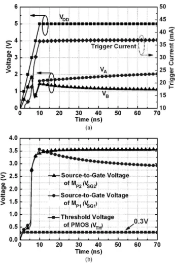
Fig. 6(a) shows the simulated transient waveforms of the new ESD-detection circuit under the normal VDD power-on
transition with a rise time of 0.1 ms. With the power-supply voltage of 1 V, the overall simulated leakage current of the new ESD-detection circuit after the VDDpower-on transition is only
about 104 nA at 25◦C. Fig. 6(b) shows the simulated source-to-gate (VSG) voltages of MP 1 and MP 2 under the normal VDD
power-on transition, whereas a threshold voltage of 0.3 V for the PMOS in the selected CMOS process is also drawn in the figure for reference. Under the normal power-on transition, VA
and VBcan follow the VDDvoltage in time without causing any
source-to-gate voltage to turn on MP 1and MP 2.
B. Operation Under ESD-Stress Condition
Prior to the ESD event, the capacitor should have no voltage across it, and the nodes VA and VB have the same voltage
levels (∼0 V) at the beginning of the ESD event. Therefore, the PMOSs MP 1and MP 2have the ability to initially turn on.
Moreover, due to the fast transient of the ESD pulse, the voltage division divided by R1, MCAP, and parasitic capacitor (CP)
provides relatively low voltage levels at VAand VB. With the
gate voltages (VAand VB) at relatively low voltage levels (as
Fig. 7. Simulated transient waveforms on the (a) node voltages and (b) source-to-gate voltages of MP 1and MP 2in the new proposed ESD-detection circuit
under ESD-like transition.
compared to the ESD voltage applied at the VDD node with
the fast rising voltage waveform), the source-to-gate voltages (VSG) of MP 1and MP 2will be quickly raised up during ESD
stresses. When VSGis greater than the MOS threshold voltage
(VTH), the PMOSs MP 1and MP 2can be turned on to generate
the desired trigger current to the trigger on the STSCR and also the MN 2. When MN 2is turned on, VBis kept at a low voltage
level.
Due to the leaky MCAP, the voltage at VA is also kept at
a low voltage level (as compared to the ESD voltage applied at the VDDnode with the fast rising voltage waveform). Therefore,
MP 1and MP 2can be continually kept in a turned-on condition
to inject the trigger current into the Vtrig of the STSCR.
Consequently, the turned-on STSCR provides a low-impedance path. Thus, the ESD current is mainly discharged through the turned-on STSCR from VDD to VSS. Something that is worth
to be mentioned is that, by using the leaky MOS capacitor in the new ESD-detection circuit, the new proposed circuit can continually provide the trigger current into the STSCR. With such a circuit arrangement, the leakage current of the leaky MOS capacitor becomes one advantage of the ESD-detection circuit under an ESD-stress condition.
Fig. 7(a) shows the simulated voltage waveforms and the trigger current of the new detection circuit under an ESD-like stress condition. When a 5-V voltage pulse with a 10-ns rise
Fig. 8. Traditional power-rail ESD clamp circuit with the STSCR as the ESD clamp device.
Fig. 9. Modified power-rail ESD clamp circuit with the PMOS restorer(MPR) and the STSCR as the ESD clamp device.
time and a 100-ns pulsewidth is applied to VDDwhich emulates
the rising edge of the ESD event before a device junction break-down, the new ESD-detection circuit successfully injects the trigger current into the STSCR. The simulated trigger current is about 37 mA, which is large enough to trigger on the STSCR. Fig. 7(b) shows the simulated voltage waveforms on the source-to-gate voltages (VSG) of MP 1 and MP 2 under an ESD-like
stress condition. With the fast-raising ESD voltage at VDD, the
VSGof MP 1and MP 2is instantly raised to be greater than the
VTHof 0.3 V. Thus, MP 1and MP 2can be immediately turned
on to conduct the trigger current into the Vtrig of the STSCR
under an ESD stress condition. The simulations are performed by the HSPICE with the gate leakage model (BSIM4) provided from the foundry, also including all parasitic capacitances of every device in the ESD-detection circuit.
IV. EXPERIMENTALRESULTS
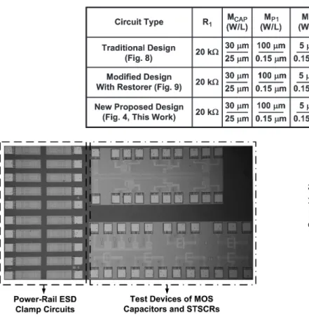
The new proposed low-leakage power-rail ESD clamp circuit (shown in Fig. 4), the traditional power-rail ESD clamp circuit with the STSCR as an ESD clamp device (shown in Fig. 8), and the modified power-rail ESD clamp circuit with the PMOS restorer and the STSCR as the ESD clamp device (shown in Fig. 9) have been drawn in the same test chip and fabricated in the same wafer of a 65-nm 1-V CMOS process. All the devices used in this paper are fully silicided thin-oxide (1-V) de-vices without using the additional silicide-blocking mask. The device dimensions used in these three power-rail ESD clamp circuits are listed in Table II, and these three designs have the same RC constant. The chip photograph of the fabricated power-rail ESD clamp circuits and test devices is shown in Fig. 10. Each power-rail ESD clamp circuit drawn in the layout
format of an I/O cell library occupies the same cell area of 30 μm× 110 μm. The layout top views of these three power-rail ESD clamp circuits in the I/O cell layout format are shown in Fig. 11. Since the MOS capacitor is directly connected to
VSS in the traditional power-rail ESD clamp circuit and in the
modified design with the PMOS restorer, an NMOS capacitor is used in this paper, as shown in Figs. 8 and 9. However, the PMOS capacitor is used in the new proposed low-leakage power-rail ESD clamp circuit because the VAand VBvoltages
of the MOS capacitor will be charged to VDD under normal
circuit operating conditions, as shown in Fig. 4.
A. DC Characteristics of STSCR
All of the power-rail ESD clamp circuits implemented in this paper use the same STSCR with identical device layout and di-mensions, as shown in Fig. 5. Fig. 12(a) shows the measured dc
I–V curves (by a curve tracer) of the stand-alone STSCR. The
trigger voltage (Vt1) is around 12 V, and the holding voltage
is 2 V (1.8 V) at 25◦C (125◦C). Since the holding voltage of the STSCR is higher than the power-supply voltage of 1 V, the latchup issue will not happen in 1-V IC applications even in the high-temperature environments. To effectively protect the internal circuits, the ESD-detection circuit is designed to inject the trigger current to lower the Vt1of the STSCR under an
ESD-stress condition. Fig. 12(b) shows the measured dc I–V curve seen from the Vtrignode to VSS. With the inherent Rsuband DP
at the Vtrignode, the stabilization of the new proposed design
can be guaranteed under normal circuit operating conditions. The measured leakage currents of the stand-alone STSCR under a 1-V bias at different temperatures are shown in Fig. 12(c). Without the thin gate structure in the SCR device, even at a high temperature of 125◦C, the leakage current of the stand-alone STSCR is only 24 nA.
B. Leakage Current
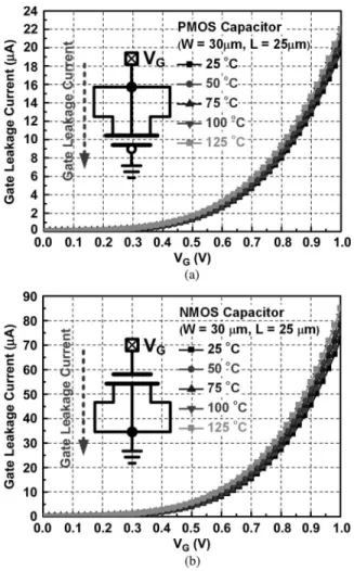
Fig. 13(a) and (b) shows the measured gate leakage currents of the stand-alone thin-oxide (1-V) PMOS and NMOS capaci-tors (W = 30 μm and L = 25 μm) with a gate-oxide thickness of∼16 Å in a 65-nm CMOS process, respectively. Under a 1-V bias across the MOS capacitor, the gate leakage currents of the PMOS capacitor and NMOS capacitor at 25 ◦C are 19.5 and 72.4 μA, respectively. With such a huge leakage current through the MOS capacitor, the traditional power-rail ESD clamp circuit will cause a huge circuit leakage which is no longer suitable in such a 65-nm CMOS process.
The measured overall leakage currents among these three fabricated power-rail ESD clamp circuits under VDD voltages
from 0.8 to 1.0 V at 25◦C and 125◦C are shown in Fig. 14(a) and (b), respectively. The leakage currents of these three power-rail ESD clamp circuits under a 1-V VDD voltage at 25 ◦C
and 125◦C are also summarized in Table III. Compared with the leakage current of the stand-alone MOS capacitor, a much higher leakage current is observed in the traditional power-rail ESD clamp circuit (see Fig. 8), where the total leakage current is around 613 μA at 25 ◦C. This result indicates that the leaky MOS capacitor certainly causes other leakage paths in
TABLE II
DEVICEDIMENSIONS INEACHPOWER-RAILESD CLAMPCIRCUIT
Fig. 10. Chip photograph of the fabricated power-rail ESD clamp circuits and test devices.
Fig. 11. Layout top views of these three fabricated power-rail ESD clamp circuits. (a) Traditional design. (b) Modified design with restorer. (c) New proposed design.
the traditional ESD-detection circuit, which, in turn, generates more leakage currents. Although the leakage current is reduced in the modified power-rail ESD clamp circuit with the PMOS restorer (see Fig. 9), it is still as high as 88 μA under a 1-V
VDDbias at 25◦C. Compared with the traditional design and
the modified design with the restorer, the new power-rail ESD clamp circuit proposed in this paper (see Fig. 4) has the lowest leakage current of only 116 nA and 1.08 μA at 25 ◦C and 125 ◦C, respectively. The leakage currents among these three
Fig. 12. (a) DC I–V curves from anode to cathode (by a curve tracer). (b) DC
I–V V curve seen from the Vtrignode to VSS. (c) Leakage current under 1-V
bias of the fabricated STSCR in a 65-nm 1-V CMOS process.
power-rail ESD clamp circuits under a VDD voltage of 1 V at
different temperatures are compared in Fig. 15. From 25 ◦C to 125 ◦C, the leakage current of the new proposed design is two orders smaller than the traditional design and the modified
Fig. 13. Measured gate leakage currents of (a) PMOS capacitor and (b) NMOS capacitor fabricated in a 65-nm 1-V CMOS process under different temperatures.
TABLE III
MEASUREDLEAKAGECURRENTS ANDHBM/MM/CDM ESD ROBUSTNESS
AMONG THEFABRICATEDPOWER-RAILESD CLAMPCIRCUITS
design with the restorer. According to the measured results, the new proposed design has the best capability to suppress the leakage current of the power-rail ESD clamp circuit in the nanoscale CMOS technology.
C. Turn-On Verification
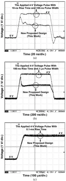
To verify the ESD-transient-detection function, the experi-mental results are shown in Fig. 16, wherein the voltage pulse is generated from a pulse generator (Hp 81110) with different rise times. In Fig. 16(a), a 4-V voltage pulse with a 10-ns rise time and a 100-ns pulsewidth is applied to VDDwith VSSgrounded to
emulate the ESD-like transient pulse. The new proposed design with an RC-time constant of 100 ns can effectively trigger
Fig. 14. Measured leakage currents among these three fabricated power-rail ESD clamp circuits at (a) 25◦C and (b) 125◦C.
Fig. 15. Measured leakage currents among these three fabricated power-rail ESD clamp circuits under different temperatures.
on the STSCR to provide a low-impedance path between VDD
and VSS. The new proposed design clamps the VDDvoltage to
around 2 V. In Fig. 16(b), a 4-V voltage pulse with a 100-ns rise time and a 1-μs pulsewidth is applied to VDD with VSS
grounded to emulate the ESD-like transient pulse whose rise time was slowed down by the on-chip decouple capacitor across the power rails. The new proposed design can also trigger on the STSCR to clamp the VDDvoltage around 2 V. In Fig. 16(c),
Fig. 16. Turn-on verification of the new proposed design under the 4-V voltage pulses with (a) 10-ns rise time and 100-ns pulsewidth, (b) 100-ns rise time and 1-μs pulsewidth, and (c) 0.1-ms rise time.
VDD with VSS grounded to verify the operation of the ESD
detection circuit. With the rise time as slow as 0.1 ms, the VDD
voltage waveform in Fig. 16(c) is the same as the applied ramp voltage, so the STSCR is not triggered on by such a pulse with a slower rise time. This result can successfully verify that the new proposed design will not be mistriggered in the normal VDD
power-on transition (with a rise time longer than 0.1 ms).
D. ESD Robustness
The transmission line pulse (TLP) generator with a 100-ns pulsewidth and a 10-ns rise time was used to measure the
I–V characteristics of these three fabricated power-rail ESD
Fig. 17. TLP-measured I–V characteristics of these three power-rail ESD clamp circuits.
Fig. 18. Measured VDD and IDDwaveforms on the new proposed
power-rail ESD clamp circuit under TLU test with VCharge of (a)−120 V and
(b) +120 V.
clamp circuits in a high-current region. The TLP-measured I–V characteristics of these three power-rail ESD clamp circuits are shown in Fig. 17. The second breakdown currents (It2) of these
three power-rail ESD clamp circuits are over 5 A. Without any trigger current, the original Vt1of the STSCR device is as high
as 12 V. With the new ESD-detection circuit, the Vt1 of the
STSCR device can be significantly reduced. The low Vt1 and
high It2 of the new proposed power-rail ESD clamp circuit
Fig. 19. New proposed low-leakage power-rail ESD clamp circuit with modified design.
The human-body-model (HBM) [20], machine-model (MM) [21], and charged-device-model (CDM) [22] ESD levels of these three power-rail ESD clamp circuits are also listed in Table III. The failure criterion is defined as a 30% shift in the leakage current under a 1-V VDDbias. To perform the ESD test,
including the CDM ESD test, the power-rail ESD clamp circuits fabricated with a silicon chip size of 4000 μm× 2000 μm were wire bonded in a 40-pin dual-in-line (DIP) package. The field-induced CDM simulator is used to verify the ESD robustness of the new proposed power-rail ESD clamp circuit in the 40-pin DIP package. The ESD test results have confirmed that the new proposed power-rail ESD clamp circuit has the highest ESD level of over 8 kV in HBM, 800 V in MM, and over 2 kV in CDM.
E. TLU Test
The transient-induced latchup (TLU) test has been used to investigate the susceptibility of ICs against the noise transient or glitch on the power lines under normal circuit operating conditions. The component-level TLU measurement setup [23] can accurately simulate the ESD-induced noises on the power lines of CMOS ICs under a system-level ESD test.
The power-rail ESD clamp circuit with the latch technique was reported to enhance the circuit performance [14]. Nev-ertheless, a transient-induced latchuplike failure may happen in such a circuit structure. With the charge voltage (VCharge)
around 10 V (negative or positive) under the TLU test, the latchuplike failure on some power-rail ESD clamp circuits has been studied [24]. The new proposed low-leakage power-rail ESD clamp circuit also combined the latch technique, but it will not suffer such a latchuplike issue. Any latchuplike issue in the new proposed design will be quickly released by the Rsub
and DP at the Vtrignode of the STSCR when it is operated in
normal circuit operating conditions. The TLU measured results on the new proposed low-leakage power-rail ESD clamp circuit are shown in Fig. 18(a) and (b). After the TLU test, the VDD
voltage level is returned back to 1 V, and the IDDcurrent is kept
at 0 A. No latchuplike failure happens in such TLU verification in Fig. 18(a) and (b). Even if the VChargeis as high as 120 V
(negative or positive) in the TLU test, the latchuplike issue did not occur in the new proposed power-rail ESD clamp circuit.
F. Discussion
From the perspective on commercial IC products, to achieve strong reliability is necessary for product qualification. In order to oppose the influence of process variations and various op-eration environments, the circuit design demands more reliable considerations. Although the experimental results showed sat-isfying ESD robustness in this paper, some modifications could be added into the new proposed design to enhance the circuit ability. Fig. 19 shows a kind of modification with a gate-couple technique. When the ESD pulse is applied to the VDDwith VSS
grounded, the voltage of VCwill be coupled up and will turn on
the MN3to force the VB to a low voltage level. Therefore, the
modified design will provide a trigger current more effectively than before. With a suitable gate-couple technique design, the response capability of the new proposed design under the ESD event will be enhanced.
V. CONCLUSION
A new power-rail ESD clamp circuit designed with con-sideration of the gate leakage issue has been proposed and successfully verified in a 65-nm CMOS process by using only thin-oxide (low-voltage) devices. The leakage currents of the new proposed power-rail ESD clamp circuit are only 116 nA and 1.08 μA at 25 ◦C and 125◦C, respectively. In addition, the new proposed power-rail ESD clamp circuit achieves ESD robustness of over 8 kV, 800 V, and over 2 kV in HBM, MM, and CDM ESD tests, respectively. With a very low leakage current, high ESD robustness, and no latchuplike failure issue, the proposed power-rail ESD clamp circuit is very suitable for the whole-chip ESD protection design in IC chips implemented in advanced nanoscale CMOS processes.
ACKNOWLEDGMENT
The authors would like to thank Dr. F.-Y. Tsai and Dr. Y.-J. Chang for their technical suggestions and
Faraday Technology Corporation, Science-Based Industry Park, Hsinchu, Taiwan, for its support on the chip fabrication. The authors would also like to thank the editor and his reviewers for their valuable suggestions to improve this paper.
REFERENCES
[1] K. Nii, Y. Tsukamoto, T. Yoshizawa, S. Imaoka, Y. Yamagami, T. Suzuki, A. Shibayama, H. Makino, and S. Iwade, “A 90-nm low-power 32-kB embedded SRAM with gate leakage suppression circuit for mobile ap-plications,” IEEE J. Solid-State Circuits, vol. 39, no. 4, pp. 684–693, Apr. 2004.
[2] A. Annema, B. Nauta, R. Langevelde, and H. Tuinhout, “Analog circuits in ultra-deep-submicron CMOS,” IEEE J. Solid-State Circuits, vol. 40, no. 1, pp. 132–143, Jan. 2005.
[3] S. Dabral and T. Maloney, ESD and I/O Design. New York: Wiley, 1998. [4] A. Amerasekera and C. Duvvury, ESD in Silicon Integrated Circuit,
2nd ed. New York: Wiley, 2002.
[5] A. Wang, On-Chip ESD Protection for Integrated Circuits. Norwell, MA: Kluwer, 2002.
[6] S. Voldman, ESD: Circuits and Devices. New York: Wiley, 2006. [7] Y.-T. Hou, M.-F. Li, H.-Y. Yu, Y. Jin, and D.-L. Kwong, “Quantum
tun-neling and scalability of HfO2and HfAlO gate stacks,” in IEDM Tech. Dig., 2002, pp. 731–734.
[8] S. Datta, G. Dewey, M. Doczy, B. Doyle, B. Jin, J. Kavalieros, R. Kotlyar, M. Metz, N. Zelick, and R. Chau, “High mobility Si/SiGe strained channel MOS transistors with HfO2/TiN gate stack,” in IEDM Tech. Dig., 2003,
pp. 653–656.
[9] M.-D. Ker, “Whole-chip ESD protection design with efficient
VDD-to- VSS ESD clamp circuit for submicron CMOS VLSI,” IEEE Trans. Electron Devices, vol. 46, no. 1, pp. 173–183, Jan. 1999.
[10] M.-D. Ker, T.-Y. Chen, C.-Y. Wu, and H.-H. Chang, “ESD protection design on analog pin with very low input capacitance for high-frequency or current-mode applications,” IEEE J. Solid-State Circuits, vol. 35, no. 8, pp. 1194–1199, Aug. 2000.
[11] K.-M. Cao, W.-C. Lee, W. Liu, X. Jin, P. Su, S.-K. Fung, J.-X. An, B. Yu, and C. Hu, “BSIM4 gate leakage model including source-drain partition,” in IEDM Tech. Dig., 2000, pp. 815–818.
[12] W.-C. Lee and C. Hu, “Modeling CMOS tunneling currents through ultra-thin gate oxide due to conduction- and valence-band electron tunneling,”
IEEE Trans. Electron Devices, vol. 48, no. 7, pp. 1366–1373, Jul. 2001.
[13] S. Poon and T. Maloney, “New considerations for MOSFET power clamps,” in Proc. EOS/ESD Symp., 2002, pp. 1–5.
[14] J. Smith, R. Cline, and G. Boselli, “A low leakage low cost PMOS-based power supply clamp with active feedback for ESD protection in 65-nm CMOS technologies,” in Proc. EOS/ESD Symp., 2005, pp. 298–306. [15] C.-T. Wang and M.-D. Ker, “Design of power-rail ESD clamp circuit with
ultra-low standby leakage current in nanoscale CMOS technology,” IEEE
J. Solid-State Circuits, vol. 44, no. 3, pp. 956–964, Mar. 2009.
[16] P.-Y. Chiu, M.-D. Ker, F.-Y. Tsai, and Y.-J. Chang, “Ultra-low-leakage power-rail ESD clamp circuit in nanoscale low-voltage CMOS process,” in Proc IEEE Int. Rel. Phys. Symp., 2009, pp. 750–753.
[17] O. Quittard, Z. Mrcarica, F. Blanc, G. Notermans, T. Smedes, and H. Zwol, “ESD protection for high voltage CMOS technologies,” in Proc.
EOS/ESD Symp., 2006, pp. 77–86.
[18] M. Dunga, W.-W. Yang, X.-M. Xi, J. He, W.-D. Liu, K.-M. Cao, X.-D. Jin, J. Ou, M.-S. Chan, A. Niknejad, and C. Hu, BSIM4v6.1 MOSFET Model Users’ Manual, [Online]. Available: http://www-device. eecs.berkeley.edu/~bsim3/bsim4.html
[19] M.-D. Ker and K.-C. Hsu, “Overview of on-chip electrostatic discharge protection design with SCR-based devices in CMOS integrated circuits,”
IEEE Trans. Device Mater. Rel., vol. 5, no. 2, pp. 235–249, Jun. 2005.
[20] Electrostatic Discharge Sensitivity Testing—Human Body Model (HBM)—Component Level, ESD Association Standard Test Method ESD
STM-5.1-2001, 2001.
[21] Electrostatic Discharge Sensitivity Testing—Machine Model (MM)—
Component Level, ESD Association Standard Test Method ESD STM-5.2,
1999.
[22] Electrostatic Discharge Sensitivity Testing—Charged Device Model
(CDM)—Component Level, ESD Association Standard Test Method ESD
STM-5.3.1, 1999.
[23] M.-D. Ker and S.-F. Hsu, “Component-level measurement for transient-induced latch-up in CMOS ICs under system-level ESD considerations,”
IEEE Trans. Device Mater. Rel., vol. 6, no. 3, pp. 461–472, Sep. 2006.
[24] M.-D. Ker and C.-C. Yen, “Investigation and design of on-chip power-rail ESD clamp circuits without suffering latchup-like failure during system-level ESD test,” IEEE J. Solid-State Circuits, vol. 43, no. 11, pp. 2533– 2545, Nov. 2008.
Ming-Dou Ker (S’92–M’94–SM’97–F’08) received
the Ph.D. degree from the Institute of Electronics, National Chiao Tung University, Hsinchu, Taiwan, in 1993.
He was a Department Manager with the VLSI Design Division, Computer and Communication Re-search Laboratories, Industrial Technology ReRe-search Institute, Hsinchu. Since 2004, he has been with the Department of Electronics Engineering, National Chiao Tung University, where was a Full Professor. Since 2008, he has been the Chair Professor and Vice President with I-Shou University, Kaohsiung, Taiwan. He is also currently a Distinguished Professor with the Department of Electronics Engineering, Na-tional Chiao Tung University, and also the Executive Director with the NaNa-tional Science and Technology Program on System-on-Chip, Hsinchu. He has over 400 published technical papers in international journals and conferences in the technical field of reliability and quality design for microelectronic circuits and systems. He has proposed many solutions to improve the reliability and quality of integrated circuits. He is the holder of 165 U.S. patents and 148 Taiwan patents. He has been invited to teach and/or to consult the reliability and quality design for integrated circuits by hundreds of design houses and semiconductor companies in the worldwide IC industry. His current research interests include reliability and quality design for nanoelectronics and gigascale systems, high-speed and mixed-voltage I/O interface circuits, on-glass circuits for system-on-panel applications, and biomimetic circuits and systems for intelligent prosthesis.
Dr. Ker has been a member of the technical program committee and the Session Chair of numerous international conferences for many years. He was an Associate Editor for IEEE TRANSACTIONSON VLSI SYSTEMS in 2006–2007. He was recognized as a Distinguished Lecturer in the IEEE Circuits and Systems Society (2006–2007) and in the IEEE Electron Devices Society (2008–2010). He was the President of Foundation in the Taiwan ESD Association. In 2009, he was recognized as one of the top ten Distinguished Inventors in Taiwan.
Po-Yen Chiu (S’08) received the B.S. degree from
the Department of Electrical Engineering, Tamkang University, Taipei, Taiwan, in 2005, and the M.S. degree from the Institute of Electronics, National Chiao Tung University, Hsinchu, Taiwan, in 2008. He is currently working toward the Ph.D. degree in the Institute of Electronics, National Chiao Tung University.
His current research interests include ESD pro-tection design for CMOS integrated circuits, mixed-voltage I/O interface circuits, and analog circuit design.
![Fig. 3. Power-rail ESD clamp circuit with the PMOS restorer (M PR ) [10]. designs to reduce the leakage current have been reported [13]–[15]](https://thumb-ap.123doks.com/thumbv2/9libinfo/7690266.143248/2.891.471.805.387.551/power-circuit-restorer-designs-reduce-leakage-current-reported.webp)