國 立 交 通 大 學
材 料 科 學 與 工 程 系
奈 米 科 技 研 究 所
碩 士 論 文
以新穎設計之錐形奈米陣列展現形貌調控、高穩定性、水潔
淨及具方向異性之多功能類壁虎黏貼結構
A geometry-controllable, anisotropic, highly stable and water
cleanable gecko-like adhesive via innovative design of taper
nanohairs.
研 究 生 : 丁懷箴 Huai-Chen Ting
指導教授 : 柯富祥 教授 Prof. Fu-Hsiang Ko
以新穎設計之錐形奈米陣列展現形貌調控、高穩定性、水潔
淨及具方向異性之多功能類壁虎黏貼結構
A geometry-controllable, anisotropic, highly stable and water
cleanable gecko-like adhesive via innovative design of taper
nanohairs.
研 究 生:丁懷箴
Student:Huai-Chen Ting
指導教授:柯富祥
Advisor:Prof. Fu-Hsiang Ko
國 立 交 通 大 學
材 料 科 學 與 工 程 系 奈 米 科 技 研 究 所
碩 士 論 文
A ThesisSubmitted to Institute of Nanotechnology Department of Materials Science and Engineering
College of Engineering National Chiao Tung University in partial Fulfillment of the Requirements
for the Degree of Master
in
Nanotechnology August 2010
Hsinchu, Taiwan, Republic of China
i
Acknowledgment
感謝柯富祥教授在學生的碩士生涯期間給予適當的指導與討論,以及提供充 足的支持和實驗資源,讓我們能無後顧之憂地全心致力於研究上,於學術外與生 活上的關心,亦培養我們健全的人格,使我們不至於在實驗之中迷失了自我,在 專業領域及待人處事上都有均衡的發展。 兩年的時間,很快,快到來不及好好體驗在實驗室以外的人生,然感謝 上帝讓我在兩年的碩士生涯裡遇到了一群真誠相待,彼此教學相長的朋友,沒有 吝於相授的架子,沒有勾心鬥角的名利,就是單單的對研究或畢業?的熱忱。在 一初進實驗室時,最令我印象深刻的就是挺著一顆引以為傲的肚子在實驗室遊走 的佳典學長,雖然脾氣不太好說話又不留情面;但最想感謝的也是他,思路清晰 新穎自然不在話下,感恩的是現在有實力又願意盡心竭力的帶學弟妹的學長不多 了,讓我在實驗上窒礙難行時,仍有人能立即點出盲點所在。中書學長的報告以 及思考模式絕對是實驗室的典範之一,從他的報告以及和他的相處中著實獲益良 多。已經離開的政哲學長雖然與我沒有太多的交集,但從他幾次的報告中以及交 談裡真的透露出他對基礎科學的熱情,也重新讓我省思對學術研究的初衷及理 想。特別感謝在實驗上給予許多適時的幫助及教導且一路陪伴我們從碩班晉為博 班的好人好事代表:鄭捷學長,思想細膩、待人真誠且擁有令人做舌的知識量, 真的是實驗室的福氣。同時感謝俊琪、其昌、銘清學長在我有困難時也不吝嗇給 予幫助;坐在印度人旁邊兩年的我,也算是半個朋友吧!說實在的,在我熬夜的 時候,還好有你們讓我不覺得自己是實驗室的孤獨老人……加油!你們的努力會 有成果的。碩一的新生對實驗室的年輕氣息絕對功不可沒,傻眼不斷的韋伶,人 來就帶來歡笑的聰敏水瓶女孩莊狗狗(誤),長太高的于菱以及碩一裡唯一有男子 氣魄的大軒,相信你們在未來的路上在研究都能有所學習及貢獻。也謝謝碩二的 同伴們,藝術大師易成、善解人意想很多的丁香、覺得肉很臭的品樺和總是在我 需要時在我後面收爛攤子的崇志,在這兩年中一起互相扶持,之後要相聚,一個 都不要跑阿!同時謝謝我的室友小趙在總是給我很多沒有用的建議,但還是很窩 心!!最後,真的感謝爸媽以及姊姊、家人的支持及供應,謝謝你們總是為我禱告, 成為我需要喘息時的避風港。我一定會將有意義的人生呈現在眾人面前。ii
以新穎設計之錐形奈米陣列展現形貌調控、高穩定性、水潔
淨及具方向異性之多功能類壁虎黏貼結構
研究生:丁懷箴 指導教授:柯富祥 教授
國立交通大學材料科學與工程系奈米科技研究所 碩士班
摘 要
由壁虎腳所引起的乾式黏附力已引起了各界的關注,透過表面的粗糙度和指 向性的改變,使其擁有強大的黏附力和微弱的脫附力且可重複使用為其迷人之 處。近來,關於壁虎腳的仿生結構在理論及實驗方面的研究已被相繼提出。然而, 這些研究與自然的壁虎相比之下,有著受限於材料方面的缺點;但在我們的研究 中, 我們設計了一有效的方法來製作出創新的結構來更符合理想的乾式吸附 力。我們首次提出,以去耦兩階段硬式陽極氧化的方式,來製作出長 1.3 微米、 直徑 380 奈米的錐形陽極氧化鋁模板;經過翻模的過程後,得到了具有傾斜角度 的錐狀奈米陣列。此錐狀奈米陣列在大面積的表現上具備了出色的方向性、可重 複使用性及水潔淨的特性。與一般的柱狀奈米陣列相比,錐狀奈米陣列有更好的 穩定性和自潔淨的特性。藉由錐狀奈米陣列在各具方向性的力上亦有出色的表 現:剪力可達到每平方公分 8 牛頓之強, 而反方向的脫附力卻僅需要每平方公分 1.4 牛頓。在未來, 此優越的黏附力可被應用於爬行機器人、液晶螢幕工廠無污 染搬運系統、以及無殘留的貼紙。我們堅信, 此新穎的結構,由於其便宜的造價,iii
整合了出色的黏附力, 加之具高度穩定性和自潔淨等優點, 在新的世代裡將會 被佔有一席之地!
iv
A geometry-controllable, anisotropic, highly stable and
water cleanable gecko-like adhesive via innovative design of
taper nanohairs.
Student : Huai-Chen Ting
Advisor : Prof. Fu-Hsiang Ko
Department of Materials Science and Engineering
Institute of Nanotechnology
National Chiao Tung University
Abstract
Dry adhesion inspired by gecko‘s feet has attracted much attention because it provides strong, yet reversible attachment against surfaces of varying roughness and orientation. Recently, theoretical and experimental investigations into the field of mimicking gecko adhesives have reported; however, they suffered from some disadvantages due to materials‘ limitation compared with nature material from gecko. In this study, we designed the efficient method of an innovate structure for ideal dry adhesives. A taper anodic alumina oxide mold with a length of 1.3 μm and a diameter of 380 nm was fabricated using decoupling two-step hard-anodization process which was firstly reported by us. After molding, taper-shaped nanohair array with slanted angle was presented. The approach to fabricate angled taper nanohair arrays obtained an excellent directional, reusable, and water cleanable use in large area. The angled taper nanohair facilitated the stability and self-cleaning properties compared with pillar nanohairs. A remarkably directional force exhibited by angled taper nanohair arrays was showing here with strong shear attachment ( ~8 N/cm2) in the gripping
v
direction and easy releasing( ~1.4 N/cm2) in the reverse direction (pulled against the angled direction of hairs). The smart adhesive presented here would enable the climbing robots, cleaning transport system such as LCD factory and non-residue sticker for future generation. We believe such a novel structure which is a low-cost, brilliant adhesion; highly stable and even self-cleaning is integral and promising for the future using.
vi
Contents
Acknowledgment...i Abstract in Chinese...ii Abstract in English...iv Contents...vi List of Figures...viii List of Tables...xviChapter 1: Introduction ... 1
1.1 General Introduction ... 1 1.2 Biomimetics ... 21.3 Hybrid characteristics tape ... 6
Chapter 2: Literatures Review ... 7
2.1 Fabricated anodic alumina porous ... 7
2.1.1 Mild anodization ... 8
2.1.2 Hard anodization ... 9
2.1.3 Taper AAO ... 15
2.2 Nondestructive replication of master mold ... 17
2.2.1 PDMS ... 17
2.2.2 PUA ... 19
2.3 Gecko-inspired artificial structure mimicking ... 23
2.3.1 Dry adhesion ... 23
2.3.2 Distinctive self cleaning gecko foot ... 35
2.3.3 Gecko analysis ... 37
2.4 Motivation ... 43
Chapter 3: Experiments ... 44
3.1 General Introduction ... 44
3.2 Experimental Methods ... 46
3.2.1 Preparation of Porous Anodic Alumina ... 47
3.2.2 Nondestructive replication of master mold and method of slanted structure ... 48
3.2.3 Assaying the Specimen ... 50
3.2.4 Dry adhesive force measurement and repeating cycle on silica .... 50
vii
Chpter4 Results and Discussion ... 52
4.1 Control Factors of Fabrication of Anodic Alumina Oxide ... 52
4.2 Dry adhesive ... 58
4.2.1 Design of taper shape ... 59
4.2.2 Unidirectional force through slanted angle slanted angle ... 66
4.2.3 Self cleaning ... 74
4.2.4 Demonstration and application ... 76
Chapter 5 Conclusion ... 78
viii
List of Figures
Figure 1.1 ... 3
Water on the surface of a lotus leaf and the microscopic image of the surface of a lotus leaf.
Figure 1.2 ... 4
SEM images of (a) HCP micro hemispheres and (b), hexagonally NCP nanonipples covering an ommatidial surface.
Figure 1.3 ... 5
(a) a gecko toe. Each toe contains hundreds of thousands of setae and each seta contains hundreds of spatula. SEM micrographs (at different magnifications) of (b) the setae (ST) and (c) the spatula (SP).
Figure 2.1 ... 8
(a) Schematic drawing of the idealized structure of anodic porous alumina. (b) SEM micrographs of the bottom view of anodic alumina layers. Anodization was conducted in 0.3 M oxalic acid at 1 °C at 40 V.
Figure 2.2 ... 9
Relation between self-ordering voltages and corresponding interpore distance (d) in sulphuric (filled black circle), oxalic (squares) and phosphoric acid (filled black triangle).
Figure 2.3 ... 11
Current–time transients during HA of electropolished aluminium substrates in 0.3M H2C2O4 (1°C). The current–time transient of a conventional MA (0.3M H2C2O4,
ix
Figure 2.4 ... 11
SEM micrographs of self-ordered AAOs formed in HA. (a) HA of a mirror-finished aluminium substrate carried out using 0.3M H2C2O4 (1°C) for 160
min. (scale bars = 800 nm) (b) HA of a mirror-finished aluminium substrate carried out using 0.4M H3PO4 (-10°C, 4000 A m−2).
Figure 2.5 ... 12
Self-ordering voltages and corresponding interpore distance (Dint) in
conventional MA.The interpore distance (Dint) versus anodization voltage observed in
oxalic HA is plotted (red open circles) with the corresponding regression line (black solid line). The inset shows the schematic cross-section of the porous alumina structure with the barrier layer; Dp = pore diameter, T = thickness of the pore wall,
t
barrier = thickness of the barrier layer.Figure 2.6 ... 12
SEM micrographs of the corresponding AAO specimens formed by MA for 2 h (left column) and HA for 2 h (right column).
Figure 2.7 ... 13
(a) Scheme for the fabrication of AAO with modulated pore diameters by pulse anodization. (b) Cross-sectional TEM images of AAO formed by pulse anodization using 0.3 M H2SO4 (UMA = 25 V, τMA = 180 s, UHA = 37 V, τHA = 1 s), showing
modulated pore diameter. Dark and bright image contrast areas correspond to MA- and HA-AAO segments, respectively. (c) SEM image of 3D stacks of MA-AAO slabs. The entire MA-AAO segment slabs were delaminated from an as-prepared AAO by selective removal of HA-AAO segments using 5 wt% H3PO4 (45°C). (d) Idealized
structure of the composite microstructure.
Figure 2.8 ... 14
Expansion of aluminum during anodic oxidation. On the left the level of the unoxidized metal surface is depicted.
Figure 2.9 ... 15
Schematic representation of self-organization of cell arrangement at high-current-density and low-current-density.
x
Figure 2.10 ... 16
Schematic for preparation of anodic porous alumina mold with tapered holes. Al substrate (a) anodization (b) pore widening (c) second anodization (d) and porous alumina with tapered holes (e,f) SEM image of anodic porous alumina with tapered holes using oxalic at 40 V.
Figure 2.11 ... 18
Schematic illustration of the procedure for fabricating PDMS stamps from a master having relief structures on its surface.
Figure 2.14 ... 20
Preparation of a UV-curable mold and reaction route.
Figure 2.15 ... 21
Tensile stress-strain relationships of three materials from the UTM analysis.
Figure 2.16 ... 22
SEM and optical mocroscopic images of replication results. (a) Master pattern of 75-nm line/space polarizer, (b) Replicated pattern of (a). (c) Replicated pattern of a 100-nm line/space circuit pattern. Inset is the cross-sectional SEM image. Bar scale in the inset is 500 nm, and (d) Example of large area replication of hologram gratings.
Figure 2.17 ... 23
Snapshots of gecko attachment and detachment from a glass ceiling. Peeling is used to achieve detachment via special muscles and joint design allowing so-called digital hyperextension.
Figure 2.18 ... 24
Multi-scale combined hierarchical gecko foot hairs. As shown, millions of fine microscopic foot hairs (setae) on the attachment pads split into hundreds of nanoscale ends (spatulae).
xi
Figure 2.19 ... 25
Examples of applications of gecko-inspired dry adhesives: (a) a climbing robot and (b) a biomedical patch.
Figure 2.20 ... 26
A schematic illustration of the classification of five major fabrication approaches for artificial dry adhesives.
Figure 2.21 ... 31
SEM images of gecko-inspired high aspect ratio nanostructures by different methods. (a) Polyimide nanohair arrays fabricated by e-beam lithography, (b) Polypropylene nanohairs fabricated by casting polypropylene film into a polycarbonate filter at an elevated temperature, (c) PMMA nanohairs fabricated by sequential application of molding and drawing of a thin polymer film, and (d) h-PDMS nanohairs fabricated by molding from AAO, the scale bar is 500 nm.
Figure 2.22 ... 31
(a) An array of hierarchical pillars fabricated by soft molding Sylgard 184 on SU-8 photolithographic templates. The base-pillars have a radius of 25 mm and a height of 200 mm. The top pillars have a radius of 5 mm and an aspect ratio of 1. (b)
PU structures with a complex tip geometry prepared bysoft-lithography and capillary molding.
Figure 2.23 ... 32
Fabrication of tilted fibers and tips: (a) Example of tilted PU microfibers with tilted fiber tips, (b) Angled polypropylene nanohair arrays fabricated by molding and roll pressing, (c) PU fibrils obtained by soft-molding on SU-8 wafers patterned by inclined lithography. The fibrils have a diameter of 8 mm, and (d) Tilted PUA nanofibers fabricated by local softening of the polymer using electron-beam irradiation.
xii
Figure 2.24 ... 34
SEM images of CNT-based dry adhesives and its durability. (a,b) Micropatterned CNT arrays by photolithography and chemical vapor deposition and (c) their durability of adhesion. SEM images of the MWCNT arrays (d) before and (e) after adhesion measurements. (f) Collapsed CNT arrays after applying preload.
Figure 2.25 ... 35
Different states of superhydrophobic surfaces: (a) Wenzel‘s state, (b), Cassie‘s superhydrophobic state, (c) the ―Lotus‖ state (a special case of Cassie‘s superhydrophobic state), (d) the transitional superhydrophobic state between Wenzel‘s and Cassie‘s states, and (e), the ―Gecko‖ state of the PS nanotube surface. The gray shaded area represents the sealed air, whereas the other air pockets are continuous with the atmosphere (open state).
Figure 2.26 ... 37
(a) Model of interactions between N gecko spatulae of radius Rs, a spherical dirt
particle of radius Rp, and a planar wall. Van der Waals interaction energies for the
particle-spatula (Wps) and particle-wall (Wpw) systems are shown and D is the
particle-to-wall distance. Our results suggest that N is sufficiently great that self-cleaning results from energetic disequilibrium between the wall and the relatively few spatulae that can attach to a single particle. (b) Representative array after dirtying with microspheres. Arrow indicates a microsphere adhering to several spatula c, array from the same animal after five simulated steps. Microspheres are still present, but spatular surfaces are mostly clean (Scale bars: 10 μm).
Figure 2.27 ... 39
Effective modulus of nanohairy structure as a function of (a) slanted angle and (b,c) aspect ratio. For ensuring tacky surface, the effective modulus should become lower than 100 kPa, which meets is the Dahlquist criterion.
Figure 2.28 ... 40
Contact tips (circles) in animals with fibrillar design of attachment pads. Note that heavier animals exhibit finer adhesion structures. The scale bar represents 2mm.
xiii
Figure 3.1 ... 47
Experimental flowchart for the fabrication and analysis was divided into two parts including AAP template (upper) and tapered shape pillar structure (lower). Following SEM images by side shows the morphology.
Figure 3.2 ... 48
The schematic diagram of experimental setup for the aluminum electropolishing and anodization.
Figure 3.3 ... 49
(a) Tapered AAO master. (b) Polymer pouring. (c) UV or thermal curing, and (d) peel off from master.
Figure 3.4 ... 50
SEM image of the exposured taper shaped pillar after pressing by carbon tapes.
Figure 4.1 ... 53
SEM image of our taper shape AAO. (a) From cross section (1.4 μm). (b) Fine structure. (c) From top view with less pore widening. (d) From top view with more pore widening (380 nm).
Figure 4.2 ... 53
Current versus time during HA in 0.25M H3PO4 (-100C). A conventional MA
(0.25M H3PO4, 160V) is also plotted (blue line) for comparison.
Figure 4.3 ... 54
SEM images of taper AAO with different lengths. (a) 600 nm. (b) 1.1 μm. (c) 1.8 μm and (d) 2.3 μm.
Figure 4.4 ... 55
Processing anodization in phosphoric acid with different concentration. (a) 1% which cannot offer enough ionic species. (b) 5% (c) 10% with excess jeoul heat from current densities. (d) 2.5% and (e) top view of AAO in 10% concentration.
xiv
Figure 4.5 ... 56
(a) to (d) Demonstrate that as voltage parameter increases, the ordered condition increases. (e) Relationship between interpore distances, current densities and voltage.
Figure 4.6 ... 57
SEM images of decoupling system. (a,b) Optimal processing widows in both first and second step. (c) Unmatched voltage cause a bad result because the applied voltage at second step is too small and (d) too big to fit the optimal condition.
Figure 4.7 ... 61
(a) Taper shaped pillars profile sketch map. (b) Pillar shape profile sketch map. (c) SEM image of taper shaped pillars and (d) illustration of taper‘s advantage.
Figure 4.8 ... 61
Force measurements versus cycles of attachment and detachment, and the force remained the same for over hundreds of time.
Figure 4.9 ... 63
Taper pillars with different lengths. (a) 600 nm from tilted SEM image (b) 600 nm from cross SEM image. (c) 1.5 μm from cross SEM image. (d) 1.5 μm from cross SEM image. The insets showed the molds of replicating or SEM images of high magnification, respectively.
Figure 4.10 ... 64
SEM images of taper and pillar nanohairs. (a) Low magnification of our structure, and the inset is the top view image that displays the taper edge and hexagonal arrays. (b) Tilted SEM image of the pillar shape showing this type cannot support the same height as the taper shape and (c) SEM image from cross. (d) Stable pillar with decreasing the length.
Figure 4.11 ... 65
Illustrate hierarchy (a) of gecko and (b) of taper shape as a hierarchy-like by “cake‖ model. (c) Illustration of Eq. 3.
xv
Figure4.12 ... 67
Displays the simulation of Eeff versus slanted angle. Clearly, the Eeff drop below
100 kPa, which fit the Dahlquist criterion, with decreasing slanted angle after 73°.
Figure4.13 ... 67
Theoretical analysis of directional adhesion mechanism of the slanted taper shaped pillars. An illustration showed the change of leaning angle of the slanted taper nanohairs when the adhesive is pulled in (a) the gripping, (b) initial state and (c) releasing direction.
Figure 4.14 ... 69
Taper shaped pillars with slanted angle we fabricated by pressure technique. (a) Low magnification. (b) High magnification of tilted SEM image of the structure. (c) Low magnification and (d) high magnification from cross view.
Figure 4.15 ... 71
Simulation of critical peeling-off forces as a function of peeling angle.
Figure 4.16 ... 71
Measurement of shear force for various cases with a adhesive patch of 1.0 cm2. The taper nanohairs were composed of soft PUA.
Figure 4.17 ... 72
Giving a comparison between taper shape and pillar shape, we can find out the higher adhesion of taper shape than pillars‘ can account for the higher density, longer length or adhere efficiently we discuss previously.
Figure 4.18 ... 73
The relationship between Pcr, diameter and Young‘s modulus (E). The graph
indicated t few effect from Young‘s modulus on Pcr, and smaller diameter is essential
xvi
Figure 4.19 ... 76
Schematic mechanism of high CA. (a) High contact angle is induced by nanostructure and low sliding angle caused by nano- and microstructures. (b,c) Illustration of the self-cleaning properties from gecko to taper shape and pillar shape adhesives. It is clearly displaying the air flowing direction which we concerned as the main reason to bring about hydrophobicity.
Figure 4.20 ... 77
Phtograph of (a) tape of PUA after replicating and the mold. (b) counter weitht measured system. (c) the high CA of tape after detaching from the glass.
xvii
List of Tables
Table 2.1 ... 21
Comparison of tensile modulus and elongation at break for three materials.
Table 2.2 ... 26
Characteristics of polymer-based dry adhesives and CNT-based dry adhesives.
Table 4.1 ... 54
MA versus HA in 2.5% H3PO4 (-10 0C).
Table 4.2 ... 60
Polymer-based gecko artificial adhesives comparison.
Table 4.3 ... 75
1
Chapter 1: Introduction
1.1 General Introduction
―There‘s plenty of room at the bottom‖ is the title of a classic talk given on December 29, 1959, in which the great physicist Richard Feynman introduced a new field of physics to the annual meeting of the American Physical Society at the California Institute of Technology. Over 40 years ago, Feynman imagined a new physical world of ultra-small volumes and highlighted some difficulties that researchers might encounter when visiting it. His talk provided a vision for engineers and scientists to establish a new field, which—with subsequent developments in novel equipment and manufacturing skills—is now known as ―nanotechnology.‖
In recent years nanotechnology has become one of the most important and exciting forefront field in physics, chemistry, engineering and biology which the characteristic dimensions are below ca. 1000 nm. It shows great promise for providing us in the near future with many breakthroughs that will change the direction of technological advances in a wide range of applications. This kind of work is often called nanotechnology. Sub-micron lithography is clearly very profitable—ask anyone who uses a computer—but it is equally clear that conventional lithographic techniques will not let us prepare semiconductor devices in which individual dopant atoms are located at specific lattice sites. Although computer hardware capability has exhibited steady exponential growth for the last 50 years—and there is a fairly widespread belief that these trends are likely to continue for at least several more years—conventional lithographic techniques are beginning to reach their limits.
As semiconductor devices become scaled down to ever-smaller sizes within the nano-regime, a variety of technological and economic problems arise, the rules of
2
classical physics give way to quantum mechanics, and the term ―molecular-scale‖ becomes more accurate than ―nanoscale.‖ At this point, the scaling of sizes that has successfully reduced device features from the microscale to the nanoscale reaches its limits, and, therefore, alternative manufacturing methods, materials, device structures, and architectures are required.
1.2 Biomimetics
Nature has gone through evolution over the 3.8 G year since life is estimated to have appeared on the Earth [1]. Nature has evolved objects with high performance using commonly found materials. These function on the macroscale to the nanoscale. The understanding of the functions provided by objects and processes found in nature can guide us to imitate and produce nanomaterials, nanodevices and processes. On nanoscale, many of the atoms are still located on the surface, or one layer removed from the surface, as opposed to the interior. Thus, different properties are observed on this scale due to the interface that is not observed in the bulk or individual atoms. Since the properties depend on the size of the structure, instead of the nature of the material, reliable and continual change can be achieved using a single material [2]. As to nanoscale structure, nature is the best teacher giving from God. Biologically inspired design or adaptation or derivation from nature is referred to as ‗biomimetics‘. It means mimicking biology or nature and is defined as ‗the study of the formation, structure or function of biologically produced substances and materials and biological mechanisms and processes especially for the purpose of synthesizing similar products by artificial mechanisms which mimic natural ones‘. Nature uses commonly found materials, and properties of the materials and surfaces result from a complex interplay between the surface structure and the morphology and physical and chemical properties. Many materials, surfaces and devices provide multifunctionality.
3
Molecular-scale devices, superhydrophobicity, self-cleaning, drag reduction in fluid flow, energy conversion and conservation, high adhesion, reversible adhesion, aerodynamic lift, materials and fibers with high mechanical strength, biological self-assembly, antireflection, structural coloration, thermal insulation, self-healing and sensoryaid mechanisms are some of the examples found in nature that are of commercial interest.
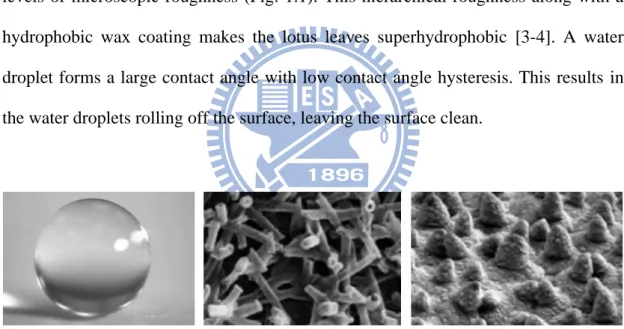
There are three areas had grab the eyes from academic and commercial field include cleaning surface, optics and adhesion. The most familiar object within the surface cleaning area for us is Lotus absolutely. The surface of lotus leaves has two levels of microscopic roughness (Fig. 1.1). This hierarchical roughness along with a hydrophobic wax coating makes the lotus leaves superhydrophobic [3-4]. A water droplet forms a large contact angle with low contact angle hysteresis. This results in the water droplets rolling off the surface, leaving the surface clean.
Figure 1.1 Water on the surface of a lotus leaf and the microscopic image of the
surface of a lotus leaf.
Moth eyes are the elite in optics area. Bernhard & Miller discovered that the outer surface of the facet lenses in moth-eyes consists of an array of cuticular protuberances termed corneal nipples. Moths use hexagonal arrays of nonclose-packed (NCP) nipples as antireflection coatings (ARCs) to reduce reflectivity from their compound eyes [5-6, 8] (Fig. 1.2). The outer surface of the corneal lenses of moths consists of
4
NCP arrays of conical protuberances, termed corneal nipples, typically of sub-300nm height and spacing. These arrays of subwavelength nipples generate a graded transition of refractive index, leading to minimized reflection over a broad range of wavelengths and angles of incidence [7]. Accordingly, it increases the transmittance, and therefore the initial interpretation of the nipple array was that it helps to enhance the light sensitivity of the light-craving moths.
Figure 1.2 SEM images of (a) HCP micro hemispheres and (b), hexagonally NCP
nanonipples covering an ommatidial surface.
A gecko is the largest animal that can produce high (dry) adhesion to support its weight with a high factor of safety. The secret of the gecko‘s adhesive properties lies in the microstructure and nanostructure of gecko feet [9-10]. Microscopy shows that gecko feet are covered with millions of small hairs called setae, which further divide into hundreds of smaller spatulas (Fig. 1.3) [11]. When such a structure is placed against any surface, hairs adapt and allow a very large area of contact with the surface. The van der Waals interaction between approximately millions setae and the substrate after contact is sufficient for the gecko to adhere and allow them to climb vertical surfaces at speeds of over 1 m, with the capability to attach or detach their toes in milliseconds. It has been suggested that this same hairy carpet on the gecko feet also
5
plays an important role in self-cleaning [12].
Figure 1.3 (a) a gecko toe. Each toe contains hundreds of thousands of setae and each
seta contains hundreds of spatula. SEM micrographs (at different magnifications) of (b) the setae (ST) and (c) the spatula (SP).
Gecko foot-hair, moth eyes and lotus surface mimicking structure were reported in ―Nature‖ and ―Science‖ in the past several times which we will have review next chapter. that shows a way to manufacture a prototype such as gecko-tape made by microfabrication of dense arrays of flexible plastic pillars with self-cleaning, re-attachable, the geometry of which is optimized to ensure their collective adhesion as shown in Fig. 1.3 which proves that the re-attachable dry adhesives based on the gecko principle can find a variety of applications.
The emerging field of biomimetics is already gaining a foothold in the scientific and technical arena. It is clear that nature has evolved and optimized a large number of materials and structured surfaces with rather unique characteristics. As we understand the underlying mechanisms, we can begin to exploit them for commercial applications.
6
1.3 Hybrid characteristics tape
Over the past few years, adhesive tapes had developed well but not enough to satisfy all. The traditional tapes are allegedly invented by the Germy Beiersdorf from a kind of polymer for hospital using in 1882. Well over decades ago, the year of 1930 can be regard as the milestone of the plastic tape, a staff from 3M named Richard Joe had invented a brand new Scotch adhesive tape bring a great reputation and establish foundation in their business field firmly. Scotch adhesive tape featured in its thin, transparent and good elastic property, becoming the sparkling star beyond their imagine without any doubt, says an exuberant manager from 3M after they became the ludicrous company. Lately, benefited from academic and industrial perennial research, a variety of functional tapes became available, such as the pressure sensitive, water activated, heat activated and drywall tape. However, people are still seeking a hybrid product can be reusable, easy-cleaning and sticky also. Instead of traditional coating on the tape, a resounding inspiration from gecko has revealed a new way to approach modern adhesives which contain both sticky and cleanable property. Microscopy makes gecko‘s foot isn‘t as enigmatic as we thought anymore, showing that gecko feet are covered with millions of small hairs called setae, which can induce giant adhesion by van der Waals interaction. Reusable property and high adhesion are the two biggest advantages; even self-cleaning effect as a hybrid function. Gecko‘s unique features remind human that the ingenious design from creatures is worthy to research and emulate. The hybrid products with gecko mimicking structure will be avant-garde in next decade.
7
Chapter 2: Literatures Review
2.1 Fabricated anodic alumina porous
Nanoporous anodic aluminum oxide (AAO) formed by anodization has been widely studied in more than 100 years [1-7]. Porous alumina membranes are used for the fabrication of composites in nanometer scale because of their relatively regular structure with narrow size distribution of pore diameters and interpore spacings [1]. The pore structure is a self-ordered hexagonal array of cells with cylindrical pores of variable sizes with diameter of 25 nm to 420 nm [8] with depths exceeding 100 mm depending on the anodizing conditions used. Essentially, the structure is a result of several coupled phenomena. One mechanism is a nonuniform electric field and, hence, current that arises in the porous aluminum structure as a result of topological variations. The second mechanism is either field-enhanced dissolution or increased local temperature that enhances dissolution of the bottom oxide barrier layer [1]. These coupled phenomena preferentially remove the oxide at the bottom of the pores while leaving the pore walls intact. In another hand, ―Nature‖ describes a model of AAO growth based on simple concepts of volume and charge conservation, coupled with experimentally validated descriptions of interfacial reactions and transport processes recently [9]. The resulting structure is an ordered hexagonal array of cells with cylindrical pores with cell walls composed of alumina. Nanoporous anodic aluminium oxide with self-organized hexagonal arrays of uniform parallel nanopores has been used for various applications in the fields of sensing, storage, separation, and the synthesis of one-dimensional nanostructures [10-12]. Self-ordered AAOs have been obtained by mild anodization (MA) and hard anodization (HA). Both of their advantages are utilized in our experiments.
8
2.1.1 Mild anodization
In ordinary two-step mild anodization (MA) process, the self-ordered columns of alumina nanopores can be obtained within three well-known growth regimes:
(1) Sulphuric acid (H2SO4) at 25 V for Dint (interpore distance) = 63 nm [13, 8]
(2) Oxalic acid (H2C2O4) at 40 V for Dint = 100 nm [14-16]
(3) Phosphoric acid (H3PO4) at 195 V for Dint = 500 nm [16-17]
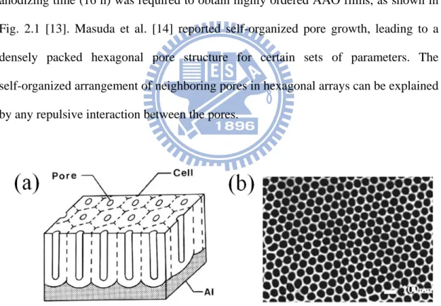
Applied voltages higher than the optimum value required to maintain stable anodization in a given electrolyte always result in ‗breakdown‘ or ‗burning‘ of the oxide film caused by catastrophic flow of electric current [18]. Therefore, a long anodizing time (16 h) was required to obtain highly ordered AAO films, as shown in Fig. 2.1 [13]. Masuda et al. [14] reported self-organized pore growth, leading to a densely packed hexagonal pore structure for certain sets of parameters. The self-organized arrangement of neighboring pores in hexagonal arrays can be explained by any repulsive interaction between the pores.
Figure 2.1 (a) Schematic drawing of the idealized structure of anodic porous alumina.
(b) SEM micrographs of the bottom view of anodic alumina layers. Anodization was conducted in 0.3 M oxalic acid at 1 °C at 40 V.
9
Figure 2.2 Relation between self-ordering voltages and corresponding interpore
distance (d) in sulphuric (filled black circle), oxalic (squares) and phosphoric acid (filled black triangle).
Fig. 2.2 shows the relationship between interpore distanceand the anodic voltage [19]. When the anodization process is outside the self-ordering regimes, the degree of spatial order decreases drastically. Both the barrier-type and pore-type AAO usually start from fairly smooth aluminum surface, but with pits formed at lattice imperfections or by electropolishing [15].
2.1.2 Hard anodization
In general, the fabrication of self-ordered Al2O3 pore arrays, under conventional
so-called ‗mild anodization‘ (MA) conditions, requires several days of processing time and the self-ordering phenomenon occurs only in narrow process windows, known as ‗self-ordering regimes‘ [8, 13-17]. Owing to the slow oxide growth rates (for example: 2–6 μm h−1), MA processes based on Masuda‘s approach have not been
10
used in industrial processes so far. Hence hard anodization (HA) of aluminum, a faster process that was invented in the early 1960s [20-21] is an attractive alternative. HA is carried out at relatively low temperatures and high current densities, and has routinely been used in the aluminum industry to produce anodic films of high technical quality at an efficient rate of production (typically 50–100 μm·h−1).
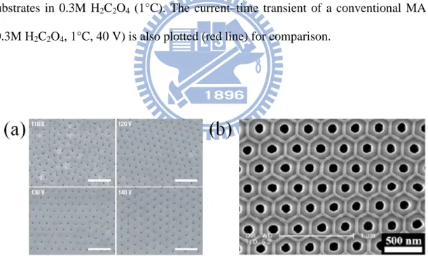
Above all, from a practical point of view, the HA process has many advantages over conventional MA. The major findings on the HA process are as follows. (1) The current density (that is, the electric field strength E at the pore bottom) is an important parameter governing the self-organization of oxide nanopores in a given anodization potential as shown in Fig. 2.3. (2) A new self-ordering regime is established over a broad range of Dint = 200–300 nm in C2H2O4 and Dint = 320 nm in
H3PO4-H2O-C2H5OH as shown in Fig. 2.4 [22]. (3) The ratio δ of the Dint to the
anodization potential is lower (δHA = 2.0 nm V−1 for HA, and δMA = 2.5 nm V−1 for MA) as shown in Fig. 2.5. (4) The porosity P is lower (PHA ~3%, PMA ~10%). (5) The growth rate of the porous oxide film is 25–35 times larger (>50 μm h−1) than for MA as shown in Fig. 2.6. (6) .Ideally ordered alumina membranes with a high aspect ratio (>1,000) of uniform nanopores can be fabricated by HA of pre-patterned aluminum. (7) Pulse anodizations of aluminum were conducted under potentiostatic conditions by using sulfuric acid or oxalic acid. Pulses consisting of a low-potential pulse followed by a high-potential pulse were applied to achieve alternating MA and HA conditions. A combination of HA and MA allows modulation of the pore diameter over extremely high aspect ratios in Fig. 2.7 [18,23].
11
Figure 2.3 Current–time transients during HA of electropolished aluminium
substrates in 0.3M H2C2O4 (1°C). The current–time transient of a conventional MA
(0.3M H2C2O4, 1°C, 40 V) is also plotted (red line) for comparison.
Figure 2.4 SEM micrographs of self-ordered AAOs formed in HA. (a) HA of a
mirror-finished aluminium substrate carried out using 0.3M H2C2O4 (1°C) for 160
min. (scale bars = 800 nm) (b) HA of a mirror-finished aluminium substrate carried out using 0.4M H3PO4 (-10°C, 4000 A m−2).
12
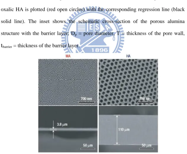
Figure 2.5 Self-ordering voltages and corresponding interpore distance (Dint) in
conventional MA.The interpore distance (Dint) versus anodization voltage observed in
oxalic HA is plotted (red open circles) with the corresponding regression line (black solid line). The inset shows the schematic cross-section of the porous alumina structure with the barrier layer; Dp = pore diameter, T = thickness of the pore wall,
t
barrier = thickness of the barrier layer.Figure 2.6 SEM micrographs of the corresponding AAO specimens formed by MA
for 2 h (left column) and HA for 2 h (right column).
13
Figure 2.7 (a) Scheme for the fabrication of AAO with modulated pore diameters by
pulse anodization. (b) Cross-sectional TEM images of AAO formed by pulse anodization using 0.3 M H2SO4 (UMA = 25 V, τMA = 180 s, UHA = 37 V, τHA = 1 s),
showing modulated pore diameter. Dark and bright image contrast areas correspond to MA- and HA-AAO segments, respectively. (c) SEM image of 3D stacks of MA-AAO slabs. The entire MA-AAO segment slabs were delaminated from an as-prepared AAO by selective removal of HA-AAO segments using 5 wt% H3PO4 (45°C). (d)
14
Figure 2.8 Expansion of aluminum during anodic oxidation. On the left the level of
the unoxidized metal surface is depicted.
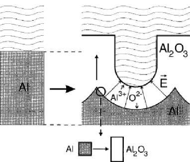
These results imply that pore initiation and the steady growth of alumina cells are strongly influenced by the high current density. In order to explain the mechanism behind pore formation phenomenon of self-organization in HA mechanism, the situation during steady state pore growth has to be considered in Fig. 2.8. Pores grow perpendicular to the surface with the equilibrium of field-enhanced oxide dissolution at the oxide/electrolyte interface and oxide growth at the metal/oxide interface [24]. While the latter is due to the migration of oxygen containing ions (O2-/OH-) from the electrolyte through the oxide layer at the pore bottom, Al3+ ions which simultaneously drift through the oxide layer are ejected into the solution at the oxide/electrolyte interface. The fact that Al3+ ions are lost to the electrolyte has been shown to be a prerequisite for porous oxide growth, whereas Al3+ ions which reach the oxide/electrolyte interface contribute to oxide formation in the case of barrier oxide growth [25].A possible origin of forces between neighboring pores is therefore the mechanical stress which is associated with the expansion during oxide formation at
15
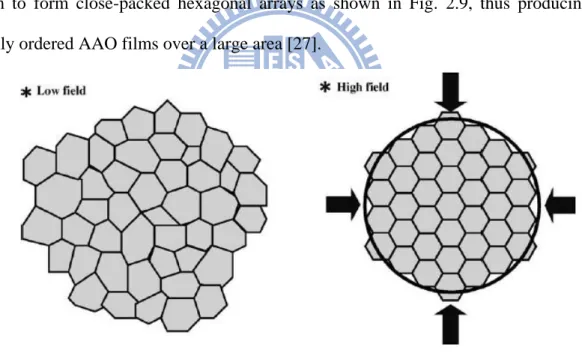
the metal/oxide interface. During the initial stages of film growth, the penetration paths that develop (which are the precursors of the regular pores) are more densely distributed due to the high anodizing current densities. Since the oxidation takes place at the entire pore bottom simultaneously, the material can only expand in the vertical direction, so that the existing pore walls are pushed upwards. Thereafter, steady film growth is attained with the development of the major pores and the repulsive interaction between the alumina cells. The repulsive interaction force, which is associated with expansion during film formation at the aluminium/oxide interface [26], increases with electric field. The strong repulsive or expansion force (high field) under high current density limited the transverse growth of alumina cells and forced them to form close-packed hexagonal arrays as shown in Fig. 2.9, thus producing highly ordered AAO films over a large area [27].
Figure 2.9 Schematic representation of self-organization of cell arrangement at high-current-density and low-current-density.
2.1.3 Taper AAO
The anodic porous alumina, which is formed by Al anodization in acidic solution, is a typical self-ordered material. Under appropriate anodization conditions,
16
long-range-ordered anodic porous alumina with an ideally pore size can be obtained. The shape of the holes in the anodic porous alumina can be controlled by a process composed of a series of anodization and subsequent etching treatments (H3PO4) as
shown in Fig. 2.10. By using the anodic porous alumina with shape-controlled holes as a mold for the replication, the preparation of AR structures of polymer could be achieved [28].
Figure 2.10 Schematic for preparation of anodic porous alumina mold with tapered
holes. Al substrate (a) anodization (b) pore widening (c) second anodization (d) and porous alumina with tapered holes (e,f) SEM image of anodic porous alumina with tapered holes using oxalic at 40 V.
17
2.2 Nondestructive replication of master mold
Nondestructive replication usually contains two methods. One is thermal curable include hot embossing like PMMA which is relatively ―hard‖ and casting like PDMS [29], another one is photo- or UV- curable material like polyacrylate [30] which may contain the photo initiator.
Microcontact printing and molding have several important advantages over other techniques for the transfer of patterns. First, this transfer is not subject to a diffraction limitation, providing access to sub-micrometer features without complicated optical or electron-beam lithography. Second, application of the stamp is direct and simple. Pattern transfer occurs simultaneously over the entire surface of the stamp, allowing a high speed of transfer compared to electron-beam or scanning-probe methods, while having a resolution approaching that of these techniques. Third, the flexibility of elastomers allows their application to non-planar substrates not obviously patternable by other techniques [31].
2.2.1 PDMS
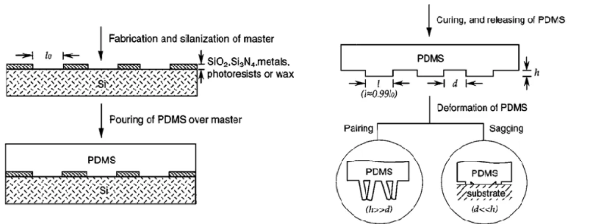
Poly(dimethylsiloxanes) have a unique combination of properties resulting from the presence of an inorganic siloxane backbone and organic methyl groups attached to silicon. They have very low glass transition temperatures and hence are fluids at room temperature. These liquid materials can be readily converted into solid elastomers by cross-linking as shown in Fig. 2.11 [32].
18
Figure 2.11 Schematic illustration of the procedure for fabricating PDMS stamps
from a master having relief structures on its surface.
Soft lithographic techniques with PDMS are currently most useful for patterning features and for fabricating structures on the size scale of 500 nm and larger. The extension of these methods to produce structures in the sub-100-nm range is limited in part by the low elastic modulus of the form of poly(dimethylsiloxane) most commonly used in fabricating stamps (Sylgard 184 PDMS) [33]. Furthermore, there‘s a approach called soft-mold-induced self-construction (SMISC), which use both electrostatic forces and surface tension difference, to facilitate the pattern growth by microwave as shown in Fig. 2.12 [34].
19
Figure 2.12 Schematic illustration of (a) soft mold imprinting under a force field and (b) SMISC by microwave.
2.2.2 PUA
Polyurethane acrylate (PUA) is a modulus-tunable ultraviolet curable mold that can provide a rigidity high enough for fine and dense features with a high aspect ratio and yet a degree of flexibility for a conformal contact over a non-flat, large area. The mechanical properties of the mold can be tailored by the chain length of an acrylate modulator in the cross-linking reaction. This tunability can be utilized to obtain a proper balance that is needed for a given patterning technique between the rigidity requirement (tensile modulus = 320 MPa) of a mold for patterning a fine structure and the flexibility requirement (tensile modulus = 19.8 MPa) for a conformal contact. The UV-curable mold consists of a functionalized prepolymer with acrylate group, a photoinitiator, and a radiation-curable releasing agent for the surface activity. Fig. 2.14 [35] gives the chemical formulas of the species involved and the reaction route to preparing the mold material. The excellent characteristic properties of the mold
20
suggested in this study are a result of the fact that the prepolymer contains both cycloaliphatic and linear long chains. The former provides the rigidity while the latter does the flexibility.
Figure 2.14 Preparation of a UV-curable mold and reaction route.
Most polymer materials are brittle materials, which fail at small values of strain, which means the polymer will break instantly once the ratio of stress to strain across over the tensile modulus(Young‘s Modulus). The mechanical properties of the two types of PUA molds, hard and soft, were determined by universal testing machine (UTM, LR10K, Lloyd Instruments, England) with the molds prepared in the form of
21
nonpatterned sheets for the tensile modulus and elongation at break. As shown in the Table 2.1 and Fig. 2.15 [30], the usual PDMS of Sylgard 184 has a good elongation property that allows excellent processing characteristics such as spontaneous wetting. On the other hand, the modulus is too low to support the mold structure in sub-micrometer range, typically for dense or high-aspect-ratio patterns.
Figure 2.15 Tensile stress-strain relationships of three materials from the UTM
analysis.
Table 2.1 Comparison of tensile modulus and elongation at break for three materials.
To enhance the mechanical integrity and thereby extend the patterning capability to smaller feature sizes, a modified hard PDMS (tensile modulus = 8.2 MPa, elongation at break = 7%) [36-37] has been introduced. Nevertheless, comparison of
22
the mechanical properties of the soft PUA mold in Table 2.1 and those of the hard PDMS mold suggests that the conformal contact should be better because the soft PUA is much more flexible, despite its higher tensile modulus, due to its higher elongational property than that of hard PDMS. On the other hand, the high modulus of the hard PUA mold in Table 2.1 implies that the mold could withstand the pressure applied for imprinting as shown in Fig. 2.16. Therefore, the material is adequately hard yet flexible enough for molding. In our approach, we utilize the soft PUA as its mechanical property is proper than others.
Figure 2.16 SEM and optical mocroscopic images of replication results. (a) Master
pattern of 75-nm line/space polarizer, (b) Replicated pattern of (a). (c) Replicated pattern of a 100-nm line/space circuit pattern. Inset is the cross-sectional SEM image. Bar scale in the inset is 500 nm, and (d) Example of large area replication of hologram gratings.
23
2.3 Gecko-inspired artificial structure mimicking
Van der Waals forces are unspecific and therefore omnipresent between practically any solid surfaces; the reason why we do not experience them in everyday life is their extremely short range: the surfaces have to be in intimate contact over large areas to exert strong forces. Nature utilizes these forces in animal locomotion. The prime example, which has aroused scientific interest especially over the last decade, is the adhesion and friction of the gecko pad for example during running, climbing, and traversing ceilings. It is now known that the gecko owes its extreme reversible adherence to a fine structure of hierarchically arranged fibrils, which enable it to exploit van der Waals and capillary forces with great efficiency as shown in Fig.2.17 [38-41].
Figure 2.17 Snapshots of gecko attachment and detachment from a glass ceiling.
Peeling is used to achieve detachment via special muscles and joint design allowing so-called digital hyperextension.
2.3.1 Dry adhesion
Dry adhesion mechanism in gecko lizards has attracted much attention since it provides strong, yet reversible attachment against surfaces of varying roughness and
24
orientation. Such unusual adhesion capability is attributed to arrays of millions of fine microscopic foot hairs (setae), splitting into hundreds of smaller, nanoscale ends (spatulae), which form intimate contact to various surfaces by van der Waals forces with strong adhesion (10 N/cm2) as shown in Fig. 2.18 [38, 40]. Recent advances of nanofabrication via top-down and bottom-up approaches have made it possible to develop synthetic, high-performance dry adhesives based on a range of different materials. Of these, polymeric nanohairs and carbon nanotubes (CNTs) have been largely used as attachmenttip materials, since they allow for robust, high aspectratio (AR) structures in a simple and reproducible manner [44-47, 48-49]. In fact, researchers have already demonstrated that artificial dry adhesives can be applied to climbing robot [50]and biomedical patch [51], as illustrated in Fig. 2.19.
Figure 2.18 Multi-scale combined hierarchical gecko foot hairs. As shown, millions
of fine microscopic foot hairs (setae) on the attachment pads split into hundreds of nanoscale ends (spatulae).
25
Figure 2.19 Examples of applications of gecko-inspired dry adhesives: (a) a climbing
robot and (b) a biomedical patch.
In this section, we aim to provide an overview of recent advances in artificial dry adhesives with nanoscale (submicron) structured materials, with emphasis on polymeric nanohairs and CNTs. A variety of synthetic dry adhesives that are based on the above two materials are outlined with their structural characteristics as well as adhesion properties.
Fabrication methods
For fabricating gecko-inspired artificial dry adhesives, a number of methods have been proposed, which can be classified into two main streams: polymer-based dry adhesives and carbon nanotube (CNT)-based dry adhesives. These two kinds of adhesives have been developed independently by utilizing different fabrication principles (Fig. 2.20). In general, the polymer-based adhesives have been fabricated by a top-down approach. For example, conventional topdown nanofabrication techniques such as electron-beam lithography, photolithography and etching techniques were utilized for fabricating nanohairs directly from a substrate [44]. In
26
parallel, polymer molding techniques were adopted by using a master with straight nanoholes [42, 45, 47, 52]. As to CNT-based dry adhesives, a bottom-up approach in which the CNT arrays were grown from the catalyst layer deposited on a substrate by chemical vapor deposition (Fig. 2.20) [18-19, 55-56]. Due to different process characteristics and materials properties used in the fabrication, the polymer-based and the CNT-based dry adhesives demonstrate different adhesion capability and parameters, which are summarized in Table 2.2.
Figure 2.20 A schematic illustration of the classification of five major fabrication
approaches for artificial dry adhesives.
Table 2.2 Characteristics of polymer-based dry adhesives and CNT-based dry adhesives.
27
One of the biggest advantages of the polymer-based methods is that they offer a simple and scalable approach to fabricating gecko-mimicking nanohairs with tailored geometry (angle, radius, height, shape of tip and hierarchy) and tunable material properties (modulus, surface energy, etc.) in a fast and cost-effective manner. Large area fabrication can be also achievable with the polymer-based approaches. The adhesion strength, however, is usually lower than that of the CNT-based adhesives because the resolution and AR of polymer nanostructures are restricted by low mechanical strength of polymer materials. In contrast, the CNT-based dry adhesives usually have high level adhesion strength since the CNTs have superior structural features such as high AR, extremely small radius (10 nm) and high modulus (1000 GPa) [48-49]. Despite these advantages, the CNT-based methods are potentially limited by complicated process for CNT growth and small patterning area (4mm×4mm) [48, 55]. Several exemplary works are in order to demonstrate how nanofabrication methods have been utilized to achieve synthetic dry adhesive with these two materials.
1. Polymer-based dry adhesive:
The gecko‘s high AR nanohairy structures can maximize the contact area by a large number of pillars at the time of contact and a smaller effective modulus, which in turn increases the adhesion force against various surfaces. To achieve high AR structures, Geim et al. presented a prototype of gecko tape having polyimide nanohairs (as small as 200 nm diameter) fabricated by e-beam lithography [44]
(categorized into ‗‗method i‘‘ in Fig. 2.20). By fabricating high AR polyimide hairs (see Fig. 2.21a), relatively high normal adhesion (3 N/cm2) was obtained. The slow and expensive process of e-beam lithography, however, is a major shortcoming of this approach. In this work, they reported that the flexibility of the substrates was a crucial
28
factor for obtaining high pull-off force. In these studies, researchers demonstrated that a small thickness of the substrate enhances the actual adhesion significantly as it allows flexibility and equal load sharing and prevents edge stress concentration [57]. After the work by Geim et al., alternative approaches have been developed to overcome the limitations of e-beam lithography. The proposed approaches are mostly based on nanomolding methods, as they allow for a facile process with minimal time and cost. In these methods, various substrates (e.g., Si, SiO2, poly-Si, AAO,
polycarbonate film, etc.) having nanoholes are prepared by e-beam lithography, photolithography, etching or electrochemical reactions. Subsequently, nanohairs are replicated by molding polymers against the substrates, as illustrated in ‗‗method ii‘‘ in Fig. 2.20. As opposed to the ‗‗method i‘‘, the fabricated substrates can be re-used as a template for nanomolding, allowing for significant reduction of time and cost. For example, Majidi et al. reported polypropylene nanohairs (see Fig. 2.21b) [46]. The hairy structures were fabricated by casting polypropylene film into a commercially available polycarbonate filter at an elevated temperature (at 200°C for 25 min) in a vacuum condition. In spite of high elastic modulus (1GPa) of the polypropylene, the hair arrays exhibited the coefficient of friction greater than 5 N/cm2 due to the enhanced compliance of the high AR nanostructures. Anodic alumina oxide (AAO) also has been utilized as a mold for generating high AR polymer nanohairs. The AAO template has highly ordered nanoholes whose diameters and depths can be easily controlled by varying the electrochemical parameters without the need of expensive e-beam or photolithography. Cho et al. presented a gecko mimicking adhesives by molding from AAO but with a low adhesion as shown in Fig. 2.21d (0.05 N/cm2). High AR polymer nanostructures could be easily obtained by simply molding the templates with thermoplastic or UV cured polymers [42, 52]. However, the resulting nanohairs molded from the AAO usually suffer ,from self-matting problem due to wet
29
chemical etching during template release or too high packing density and AR of the nanostructures, which diminishes the resulting adhesion force significantly [42, 52]. Jeong et al. suggested a nanodrawing method for fabricating high AR polymer nanohairs (80nm diameter, 2 μm height and AR > 20) on a solid substrate by sequential application of molding and drawing of a thin polymer film with 3 N/cm2 (see Fig. 2.21c) [45].
Hierarchical structures with stacked fibers of different dimensions were recently fabricated by different methods. Well-defined arrays of hierarchical microfibrils were obtained by multistep photolithography using SU-8 [58]. Molding with PDMS via a adequate mold rendered fibrils with AR of 4 (25 μm diameter) on top of fibrils with AR up to 1 (5 μm diameter; Fig. 2.22a) [53, 58]. Two-step molding has also been used to fabricate PU hierarchical structures: the base fibers were formed by softlithography, while the top ones were formed by capillary molding and a second curing step (the first level of fibrils were 5 to 50 mm in diameter and 25 to 100 mm high; the second-level fibers were 350 nm to 3 mm in diameter and 2.8 to 20 mm high; Fig. 2.22b) [59].Interestingly, these hierarchical hairs maintained their adhesive force even on a rough surface due to an increase in the contact area bythe enhanced height of hierarchy, whereas simple nanohairs lost their adhesion strength, demonstrating the usefulness of hierarchical structures against rough surfaces. Nevertheless, most of them reported are without a large enough adhesion and directional force.
Fibrillar surfaces with a slanted angle show smaller effective elastic modulus than planar surfaces. As a result, they deform easily and form contact effectively, especially when adhering to rough substrates. The elastic-strain energy stored in slanted single fibrils during pull-off is dissipated and, as a consequence, the separation work is higher than for a planar contact of similar material [43, 60]. From the point of view of fracture mechanics, fibrillar structures with a slanted angle require frequent
30
re-initiation of the interface crack and the failure of the interface therefore occurs at higher stresses [60]. As shown in Fig. 2.23a, spatular tips at angles between 0 and 900 with respect to the substrate were obtained on tilted PU fibers by applying a controlled load to the tilted fibrils during curing, causing bending of the fibrils [54]. This design, containing two independent tilted components (fiber and spatula), represents the most complex structure obtained to date with artificial systems. Slanted fibrillar structures were obtained by double replication of tilted SU-8 fibrillar arrays obtained by photolithography (Fig. 2.23c). This process involved tilted exposure of the resist layer to obtain fibrils forming angles between 0 and 500 with the substrate and exhibiting dimensions of 4 to 35 μm indiameter and ARs of up to 10. A mold of silicone rubber containing angled holes is then fabricated by soft-molding against the SU-8 template and subsequently used to obtain PU microfibers from liquid precursors [61]. Alternatively, arrays of PP microfibers were fabricated by first filling PC membranes with PP to obtain vertical fibrils and then tilting them by processing the patterned film through two heated rollers (Fig. 2,23b) [62]. Tilted fibrils with 0.6 mm diameter, 18 to 20 mm length, and a 45° tilting angle were obtained. Coarser structures with 1mm length, 380 μm diameters and a tilt angle of 20° with a top face inclined at 450 with respect to the vertical were obtained by casting a PU precursor onto a mold fabricated by micromachining. Tilted structures were also prepared by a post-molding electron-beam irradiation step. The irradiated fibril surfaces shrink more than the opposite surface, resulting in bending of soft-molded fibrils [47]. With this method, PUA nanopillars (100 nm in diameter and with an AR of 10) were fabricated with tilting angles between 30° and 80° (Fig. 2.23d).
31
Figure 2.21 SEM images of gecko-inspired high aspect ratio nanostructures by
different methods. (a) Polyimide nanohair arrays fabricated by e-beam lithography, (b) Polypropylene nanohairs fabricated by casting polypropylene film into a polycarbonate filter at an elevated temperature, (c) PMMA nanohairs fabricated by sequential application of molding and drawing of a thin polymer film, and (d) h-PDMS nanohairs fabricated by molding from AAO, the scale bar is 500 nm.
32
184 on SU-8 photolithographic templates. The base-pillars have a radius of 25 mm and a height of 200 mm. The top pillars have a radius of 5 mm and an aspect ratio of 1.
(b) PU structures with a complex tip geometry prepared by soft-lithography and
capillarymolding.
Figure 2.23 Fabrication of tilted fibers and tips: (a) Example of tilted PU microfibers with tilted fiber tips, (b) Angled polypropylene nanohair arrays fabricated by molding and roll pressing, (c) PU fibrils obtained by soft-molding on SU-8 wafers patterned by inclined lithography. The fibrils have a diameter of 8mm, and (d) Tilted PUA nanofibers fabricated by local softening of the polymer using electron-beam irradiation.
2.CNT-based dry adhesives
33
and b) [48]. Interestingly, they reported that micropatterned CNT arrays with optimized geometry have four to seven times higher shear adhesion (~36 N/cm2) strength than nonpatterned CNT arrays. Moreover, the adhesion strength was maintained over thousands of cycles (Fig. 2.24c). Qu et al. also reported similar adhesion strength (15 N/cm2 shear adhesion and 30 N/cm2 normal adhesions) by growing single walled CNTs (SWCNTs) [63]. Following this work, they further enhanced the performance of the dry adhesive using MWCNTs [49]. With use of vertically aligned MWCNT having curly entangled end segment, they could obtain extremely high shear adhesion (~100 N/cm2), which was ten times higher than gecko‘s adhesion strength (Fig. 2.24d and e). The strong shear adhesion comes from shear-induced alignment of the nonaligned top layer of the nanotubes enhancing the contact line length (Fig. 2.24e) [49]. As a result, increasing the CNT length greatly enhanced the shear adhesion. In contrast, the normal adhesion force was almost insensitive to the nanotube length as a result of point contact. Interestingly, there have been seemingly opposite reports on repeatability and robustness of CNT-based dry adhesives. Ge et al. and Qu et al. reported that CNT arrays maintained the strength for long attachment/detachment cycles whereas Zhao et al. reported that the adhesion strength was decreased with repeated use due to an interface failure between CNT arrays and the substrate [48-49]. Recently, Wirth et al. investigated the structural changes of vertically aligned CNT arrays (10 nm in diameter and 100 μm in length) after attachment [64]. They observed that the applied force for preloading leads to the collapse of the CNT arrays limiting the repeatable use of the dry adhesives, as shown in Fig. 2.24f. It seems that the interfacial strength between CNTs and the substrate is important for ensuring robustness and repeatability of the CNT-based adhesives. In general, CNT-based dry adhesives have higher adhesion strength than polymer-based adhesives due to outstanding structural properties such as extremely high AR (> 104,
34
diameters around 10nm and heights over 100 μm). With extraordinary high AR, the effective modulus of CNT is reduced below Dahlquist criterion (E ~100 kPa) in spite of its high mechanical modulus (~103 GPa) (see Fig 2.28). However, the patterned area of CNT arrays is usually small (~1.6mm2) due to the complicated process (photolithography, catalyst deposition and chemical vapor deposition at high temperature, e.g., ~750 ◦C). It is worthwhile noting in this regard that the adhesion force per area can be enhanced greatly by reducing the contact area [65]. Also, the adhesion force of single nanohair measured by AFM might be misleading as it would not scale linearly into the bulk adhesion strength. In addition to the complicated and expensive process as well as small patterning area, another major concern of the CNT-based adhesives is that it requires a high preload (50~500 N/cm2) compared to that of polymer-based adhesives (< 0.5 N/cm2), potentially limiting the widespread use of the CNT-based adhesives.
Figure 2.24 SEM images of CNT-based dry adhesives and its durability. (a), (b)