單晶片溫度感測器中的三角積分調變器之設計與製作
79
0
0
全文
(2) 單晶片溫度感測器中的三角積分調變器之設計與製作 The Design and Implementation of Sigma-Delta Modulator for CMOS Monolithic Temperature Sensors 研 究 生:吳書豪. Student:Su-How Wu. 指導教授:闕河鳴 博士. Advisor:Dr. Herming Chiueh. 國 立 交 通 大 學 電 信 工 程 學 系 碩 士 班 碩 士 論 文. A Thesis Submitted to Department of Communication Engineering College of Electrical Engineering and Computer Science National Chiao Tung University in Partial Fulfillment of the Requirements for the Degree of Master of Science in Communication Engineering July 2004 Hsinchu, Taiwan. 西元二00四年七月.
(3) ______ ____________________________________________________. 單晶片溫度感測器中的三角積分調變器之設計與製作 研究生:吳書豪. 指導教授:闕河鳴 博士. 國立交通大學 電信工程學系碩士班. 中文摘要. 本研究目的是設計出一個低功率、高準確性的類比數位轉換器,並必須具有 較大且較高的工作溫度區間。其功能是實現介於晶片型溫度感測器和內嵌控溫單 元的介面電路,因此對於使用在晶片系統上的溫度管理系統而言是相當重要的。 包括功率消耗、溫度範圍、製程相容性、、等挑戰,都使得這個類比數位轉換器 的設計變的相當困難。本論文提出一個採用台積電 0.25 微米互補式金氧半標準 製程的過取樣三角積分調變器原型晶片,其量測結果能達到八位元準位和極低功 率消耗的表現,這樣的研究成果符合溫度管理系統所需的規格。除此之外,因為 設計流程中已考慮到製程縮小的趨勢,因此對於採用更先進製程的溫管理系統也 得以實現,這使得超大型積體電路或是高集線密度的電路得以免去過熱的問題。. __________________________________________________________________ The Design and Implementation of Sigma-Delta Modulator For CMOS Monolithic Temperature Sensors. I.
(4) ______ ____________________________________________________. The Design and Implementation of Sigma-Delta Modulator for CMOS Monolithic Temperature Sensors. Student: Su-How Wu. Advisor: Dr. Herming Chiueh. Department of Communication Engineering National Chiao Tung University Hsinchu, Taiwan. Abstract In this research, a low power high accuracy analog to digital converters (ADCs) with higher and wider temperature rang is designed. The proposed design plays an important role in modern system-on-chip thermal management system, which acts as an interface circuitry between monolithic temperature sensors and thermal management unit. Several challenges exists, including temperature range, power dissipation requirements and processing technology compatibility, which cause the design of such an ADC become a difficult work. This thesis examines a practical design of oversampling ADC based on sigma-delta modulation with thermal considerations. The prototype is fabricated in a TSMC 0.25µm standard CMOS process. The experimental result achieves eight bits resolutions and dissipates only a few mw which fulfill the system requirements of targeting thermal management design. Besides these requirements, the processing scaling of proposed ADC is considered in order to be compatible with targeting SoC fabrication technology. The integration of monolithic temperature sensor, proposed ADC and thermal management unit keep the progressing trend of modern VLSI and high-density circuits without thermal problems. __________________________________________________________________ The Design and Implementation of Sigma-Delta Modulator For CMOS Monolithic Temperature Sensors. II.
(5) ______ ____________________________________________________. Acknowledgments 本篇論文得以順利完成,首先要感謝的是我的指導教授闕河鳴博士。闕老師 總在研究遇到瓶頸的時候給予寶貴的建議,使我得以突破與進步。除此之外,老 師在平日培養學生獨立思考與分析問題的能力,更使我在研究領域建立正確的態 度。. 其次,謝謝謹鴻、志軒、明治、智閔四位同窗在我研究上與生活上,給予諸 多的幫助與指教,尤其感謝智閔平日與我討論和切磋,使我釐清許多思路上的盲 點並使我基本概念更加紮實。在此也謝謝學弟、學妹們的支持與幫忙。有了各位 晶片系統設計實驗室成員的陪伴,才讓我有這麼一段快樂且充實的研究經驗。. 最後,我要感謝父母的栽培與弟妹的鼓勵,以及所有關心我的家人與朋友, 唯有藉著大家的愛護和幫忙,才能造就今日的我。. 我誠心感謝上述提攜或幫助過我的你們,謝謝大家並祝福大家。. 吳書豪 July,19,2004. __________________________________________________________________ The Design and Implementation of Sigma-Delta Modulator For CMOS Monolithic Temperature Sensors. III.
(6) ______ ____________________________________________________. Contents 中文摘要 English Abstract Acknowledgments Contents List of Tables List of Figures List of Abbreviations and Symbols. Ⅰ Ⅱ Ⅲ Ⅳ Ⅵ Ⅶ Ⅸ. Chapter1 Introduction. _________. 1.1 Motivation 1.2 Organization. 1 1 3. Chapter2 Fundamentals of SDM. _. 2.1 A Brief introduction of ADC 2.2 Quantization Noise 2.3 SDM Architecture 2.3.1 First Order SDM 2.3.2 Second Order SDM 2.3.3 Higher Order SDM 2.4 Performance Metrics. 4 4 6 10 12 13 14 15. Chapter3 System Level Design Considerations 3.1 Limitations 3.2 Higher Temperature Issues. 17 17 24. Chapter4 Implementation of Proposed Sigma Delta Modulator 4.1 Circuit Level Design 4.2 Transistor Level Design 4.2.1 Differential OPAMP 4.2.2 Comparator 4.2.3 Switches and Capacitors 4.2.4 Integrator 4.2.5 Feedback DAC 4.2.6 Output Buffer 4.3 Layout Level Design. 30 30 32 32 39 44 47 50 51 52. __________________________________________________________________ The Design and Implementation of Sigma-Delta Modulator For CMOS Monolithic Temperature Sensors. IV.
(7) ______ ____________________________________________________. 4.4 Simulation Results. 54. Chapter5 Testing Setup and Experimental Results. 56. 5.1 Testing Environment 5.2 PCB Circuits 5.3 Performance Evaluation 5.4 Summary. 56 57 60 64. Chapter6 Conclusions. ____. References. 65. __ 66. __________________________________________________________________ The Design and Implementation of Sigma-Delta Modulator For CMOS Monolithic Temperature Sensors. V.
(8) ______ ____________________________________________________. List of Tables Table 2.1 Various kinds of ADCs Table 2.2 Summarize the SNR of SDM Table 3.1 Some parameters of NMOS with level 2 model Table 4.1 Organization of SDM Table 4.2 Switches and comparators information Table 4.3 OPAMP device ratios summary Table 4.4 OPAMP simulated specifications summary Table 4.5 Comparator device ratios summary Table 4.6 Output buffer device ratios summary Table 5.1 Pin assignments Table 5.2. Performance Summary. __________________________________________________________________ The Design and Implementation of Sigma-Delta Modulator For CMOS Monolithic Temperature Sensors. VI. 4 9 25 30 31 38 38 42 51 63 63.
(9) ______ ____________________________________________________. List of Figures Figure 1.1 Building blocks of thermal management system Figure 2.1 System architectures of ADCs Figure 2.2 (a) Transfer curve of ADCs (b) Quantization noise Figure 2.3 Probability and power spectral density function of quantization noise Figure 2.4 Three kinds of ADCs Figure 2.5 The magnitude and gain of NTF Figure 2.6 The SNR of SDM Figure 2.7 Analysis of time domain and frequency domain of SDM Figure 2.8 Building blocks of oversampling ADCs used SDM Figure 2.9 A first order SDM Figure 2.10 A second order SDM Figure 2.11 Higher order SDM Figure 2.12 Static performance metrics Figure 2.13 Dynamic performance metrics Figure 3.1 A SC integrator Figure 3.2 Effects of leakage in the SCI Figure 3.3 Comparison of SCI output probability densities for different feedback factor Figure 3.4 Simulated integrator distortions Figure 3.5 (a) Equivalent model for integration mode (b) Time evolution of vo Figure 3.6 A behavior model implemented in MATLAB Figure 3.7 The sub-circuit of loop filter Figure 3.8 ZTC bias points for NMOS (14μm/0.7μm) in 0.25μm process Figure 3.9 Id, gm, gds characteristics for ZTC, ZTC+0.2v, ZTC+0.6v Figure 3.10 Leakage current components Figure 3.11 The leaky junction diodes are explicitly shown in CMOS Figure 3.12 Compensation circuits for leakage current Figure 4.1 Circuit level of SDM Figure 4.2 A timing diagram illustrating clock signals Figure 4.3 Fully differential OPAMP Figure 4.4 Small signal equivalent circuit of OPAMP Figure 4.5 Two types of the bias circuit Figure 4.6 Latch Voc by negative feedback Figure 4.7 Relationship between Vcm and Voc Figure 4.8 Frequency response of this fully differential OPAMP __________________________________________________________________ The Design and Implementation of Sigma-Delta Modulator For CMOS Monolithic Temperature Sensors. VII. 1 5 6 6 7 8 10 11 12 13 13 14 15 16 17 18 19 20 20 23 24 26 27 28 28 29 31 32 33 35 35 36 37 38.
(10) ______ ____________________________________________________. Figure 4.9 (a) A NMOS latch (b) An analogy Figure 4.10 DC analysis of a NMOS latch Figure 4.11 Equivalent models for (a) output resistance (b) time constant Figure 4.12 A regenerative comparator Figure 4.13 DC analysis of the preamplifier Figure 4.14 Transient analysis of the preamplifier Figure 4.15 (a) MOS switches (b) Output level for different switches Figure 4.16 Turn on resistance of NMOS, PMOS, and a transmission gate Figure 4.17 MIM capacitor structure and its equivalent circuit Figure 4.18 A pair of complementary SC integrators Figure 4.19 Differential SC integrators Figure 4.20 The Bode plot of SCI with present OPAMP, C1/C2=0.8, and 2Mhz clock Figure 4.21 A CDS SC integrator Figure 4.22 Feedback DAC circuit Figure 4.23 A chain of N inverters with output capacitance Figure 4.24 Redraw (a) OPAMP (b) Comparator Figure 4.25 Diagram of SDM layouts Figure 4.26 Transient Analysis of proposed SDM Figure 4.27 Power spectrum of proposed SDM (a)log scale (b)linear scale Figure 4.28 Baseband output spectrum Figure 4.29 SNDR versus input mismatch Figure 4.30 Dynamic range simulation Figure 4.31 SNDR versus temperature Figure 5.1 Experimental test setup Figure 5.2 The measurement situation Figure 5.3 The schematic of the clock generator Figure 5.4 The schematic of the voltage regulator Figure 5.5 Input terminal circuit Figure 5.6 The photograph of the whole PCB Figure 5.7 Measured input waveforms of the DUT Figure 5.8 Die micrograph Figure 5.9 Measured output waveforms of the SDM Figure 5.10 Measured output spectrum of the SDM (a) all-band (b) in-band Figure 5.11 (a) linear scale PSD (b) log scale PSD Figure 5.12 Digital output simulation. __________________________________________________________________ The Design and Implementation of Sigma-Delta Modulator For CMOS Monolithic Temperature Sensors. VIII. 39 40 41 41 42 43 44 46 46 47 48 49 49 50 51 52 53 54 54 55 55 55 55 56 57 58 58 59 59 60 61 62 62 62 62.
(11) ______ ____________________________________________________. List of Abbreviations and Symbols AC ADC Av BW CAD CDS CMFB CMOS CMRR DAC DC DFT DNL DR DSP DUT ENOB FFT fc fs Fu gm ICMR ID INL k LSB M m NTF OPAMP OSR PCB PSD PSRR. Alternative Current Analog to Digital Converter Open loop gain Bandwidth Computer-Aided Design Correlated Double Sampling Common Mode Feedback Complementary Metal-Oxide Semiconductor Common Mode rejection ratio Digital to Analog Converter Direct current Discrete Fourier Transform Differential Nonlinearity Dynamic Range Discrete-Time Signal Processing Device Under Test Effective Number Of Bits Fast Fourier Transform Input Cutoff Frequency Sampling Frequency Unit-gain Frequency Transconductance Input Common Mode Range Drain Current Integral Nonlinearity Boltzmann’s constant The Least Significant bit Oversampling Ratio m-order Sigma-Delta Modulator Noise transfer function Operational Amplifier Oversampling Ratio Printed Circuit Board Power Spectral Density Power Supply rejection ratio. __________________________________________________________________ The Design and Implementation of Sigma-Delta Modulator For CMOS Monolithic Temperature Sensors. IX.
(12) ______ ____________________________________________________. Px R rds RMS Ron S SC SCI SDM SFDR SNDR SNR SoC SR STF T THD Vds Vgs VLSI Vov Vth ZTC. Power of quantity x, i.e. Pin, Pe Capacitor Ratio CMOS output resistance Root Means Square turn-on resistance of switches Device Ratio, namely W/L Switched-Capacitor Switched-Capacitor Integrator Sigma-Delta Modulator Spurious-Free Dynamic Range Signal to Noise and Distortion Ratio Signal to Noise Ratio System On Chip Slew Rate Signal transfer function Absolute temperature Total Harmonic Distortion Drain to Source Voltage Gate to Source Voltage Very Large Scale Integrated CMOS Overdrive Voltage CMOS Threshold Voltage Zero-Temperature-Coefficient. __________________________________________________________________ The Design and Implementation of Sigma-Delta Modulator For CMOS Monolithic Temperature Sensors. X.
(13) _____________________________________________________________________________ ______Chapter1: Introduction. Chapter1 Introduction ___________________________________________________________ 1.1 Motivation Increases in circuit density and clock speed in modern VLSI design brought thermal issues into the spotlight of high-speed VLSI design [1]. Previous research has indicated that the thermal problem in modern integrated circuits can cause a significant performance decay [2] as well as reducing of circuitry reliability [3-6]. Local overheating in even one spot of high-density circuits, such as CPUs and high-speed mixed-signal circuits [7, 8] can cause the whole system crashed. The reasons include clock synchronization problems, parameter mismatches or other coefficient changes due to the uneven heat-up on a single chip [2]. In order to avoid thermal damages, early detection of overheating and properly handling such events are necessary. Recent research has proposed the utilization of a thermal management system [9, 10] for large scale integrated circuits. In such design, adapting cooling and temperature monitoring mechanisms are widely used. However, implementation of on–chip thermal management systems, as shown in Figure 1.1, consist several challenges: embedded sensors, accurate ADCs, low power circuitry, and small physical area. In order to overcome such challenges, this thesis focuses on the design and the analysis of suitable ADC for thermal manager systems. The characteristics of this ADC includes following requirements [5]: ‧ Compatibility with the target process without any additional fabrication step; ‧ Low power consumption; ‧ A reasonably wide temperature range; ‧ Small active area; ‧ Accuracy and long term stability;. References Temperature Sensor. Analog Signal. Digital Signal. ADC. Thermal Management System. Figure 1.1 Building blocks of thermal management system __________________________________________________________________ The Design and Implementation of Sigma-Delta Modulator For CMOS Monolithic Temperature Sensors. 1.
(14) _____________________________________________________________________________ ______Chapter1: Introduction. The implementation of thermal-aware ADCs in modern deep-sub-micron CMOS technology implies servile difficulties [1, 5].The most important design aspect of ADC is accuracy. The specification for conventional applications is 2 oC in a limited temperature range from -20 oC to 100 oC. Since thermal sensors has maximum inaccuracy of approximately 1 oC can be met at room temperature. Assuming that errors introduced by ADCs can be neglected, that indicates the resolution of such ADCs are higher than seven bits [11]. Nyquist rate ADCs can effectively produce digital codes without followed processing, but hard to achieve high resolution due to mismatching in CMOS process at elevated temperature, furthermore such architecture are difficult to maintain long term stability over wide temperature range. By contrast, the oversampling ADCs based on sigma-delta-modulator (SDM) structure are generally robust to several expected impairments, such as decreased amplifier open-loop gain and increased comparator offset [12]. As well as, the SDM enables nearly unlimited high resolution data conversion without precise matching due to inherent linearity one bit ADC and feedback DAC [13]. Additionally, some great benefits to accomplish SDMs in CMOS technology, for instant, circuitry are complicated by low power and a sample-and-hold circuit is not required at the input. The drawback of SDM is its low speed operation. But the thermal disturbance rate is reckoned into millisecond and the worse case of temperature sensor is specified to hundreds of samples, giving a required bandwidth of few kilo-hertz scale [11].It should be concluded that according to the trade-off between accuracy, simplicity and power consumption, the best candidate of ADC at high temperature is the SDM architecture, which consist of an analog filter and a coarse (often single-bit) quantizer connected together in a feedback loop operated in oversampling and noise shaping. In practice, the imperfections of circuits, namely leakage integrators and several noise sources must be considered in system architecture. System level design used MATLAB determines the sensitivity to analog sub-circuits, and the circuit level specifications are decided. In addition to this architecture constraint, approaches to minimize high temperature disfigurement are taken into account in transistor level design for operation correct from ambient to elevated temperature. This thesis describes the flow and results of the design and implementation of SDM for CMOS monolithic temperature sensors. The experimental SDM present herein have been fabricated in a standard 0.25µm CMOS technology, and provides 8 bits resolution at 25oC and 7 bits resolution at 125oC as well as dissipation only a few milliwatts.. __________________________________________________________________ The Design and Implementation of Sigma-Delta Modulator For CMOS Monolithic Temperature Sensors. 2.
(15) _____________________________________________________________________________ ______Chapter1: Introduction. 1.2 Organization In Chapter 2, the beginning is the overview of analog-to digital converters (ADC) consists of basic characteristics and classification. After them, quantization issues, wherein the principles of oversampling and noise shaping technology are introduced mathematically. Then diverse structures of sigma-delta modulators (SDM) and performance metrics end this chapter. Chapter 3 represents system level design considerations, including the analysis of error mechanisms, high temperature issue, design trade-offs. All of limitations can construct a behavioral modeling of SDM to determine system characteristics. Chapter 4 discusses the topics of sub-circuits that will be used to realize an actual integrated circuit, which covers an operational amplifier (OPAMP), a comparator, switches and capacitors, and the feedback path. The simulation results and device ratios are given at each section. The circuit level, transistor level, and layout level design will be described in sequence. In chapter 5, the testing environment is present, including the instruments and external testing circuits on printed circuit board (PCB). Experimental results for a SDM, which is fabricated in a 0.25µm 1P5M 3.3V standard CMOS with MIM process, will be plotted and summarized.. __________________________________________________________________ The Design and Implementation of Sigma-Delta Modulator For CMOS Monolithic Temperature Sensors. 3.
(16) ___________________________________________________________________________Chapter2: Fundamentals of SDM. Chapter2 Fundamentals of SDM ___________________________________________________________ This chapter begins with a brief overview of analog-digital converters (ADC) in the aspects of speed and architecture. Following by the classification of ADC, a quantization error is considered and defined mathematically. A subclass of oversampling ADC based on noise shaping topologies is then examined, which referred to various architectures of sigma-delta modulators (SDM). The performance metrics of targeting ADC is then described in the end of this chapter.. ___________________________________________________________ 2.1 A brief introduction of ADCs ADCs, or equivalently quantizers, are fed a continuous-time analog signal to convert discrete-levels and play the most important role in signal processing. A pre-filter called an antialiasing filter is necessary to avoid off high frequency signals back into the baseband of the ADC, is usually followed by a sample-and-hold circuit that maintain the input signal constant during the time this signal is converted to an equivalent output code. This time is called the conversion time of the ADC. Depending on its speed and accuracy, ADCs are used in signal-processing applications, for instance, video, radio, radar, and telecommunications. According to input bandwidth, there are three categories of ADCs, and are listed in Table 2.1 below. All of them are Nyquist-rate ADCs except oversampling structure, and the carefully definitions will be examined in the following section. Table 2.1 Various kinds of ADCs Category. Structure. Low-to-Medium Speed High Accuracy. Integrating Oversampling. Medium Speed Medium Accuracy. Successive approximation Algorithmic. High Speed Low-to-Medium Accuracy. Flash, Two-step, Interpolating, Folding, Pipelined, Time-interleaved. __________________________________________________________________ The Design and Implementation of Sigma-Delta Modulator For CMOS Monolithic Temperature Sensors. 4.
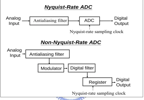
(17) ___________________________________________________________________________Chapter2: Fundamentals of SDM. In the viewpoint of system architecture shown in Figure 2.1, the Nyquist-rate ADC can cover signal directly, the relationship between digital output and analog input is one-on-one. On the contrast, non-Nyquist-rate ADCs (oversampling ADCs) need a register to store a sequence of digital output for one analog input. Another key point of non-Nyquist-rate ADCs is that, the operational frequency of the modulators and digital filters is above Nyquist-rate that is why they are called “oversampling”.. Nyquist-Rate ADC Analog Input. Antialiasing filter. ADC. Digital Output. Nyquist-rate sampling clock. Non-Nyquist-Rate ADC Analog Input. Antialiasing filter Modulator. Digital filter Register. Digital Output. Nyquist-rate sampling clock. Figure 2.1 System architectures of ADCs Assume discrete-level of a quantizer outputs are transferred to specific states by references, which has the same voltage level with input signal. It is easy to plot transfer curve, like Figure 2.2(a) next page, and this diagram helps to define several basic properties of ADCs. 1.. The number of output states can be estimated by binary and referred as N bits resolutions. Thus N bits ADCs can map input signals into 2N output levels.. 2.. The full scale input range which a quantizer can handle is called A. If the input signal exceed A, the quantizer is overload. The separation of output level is the least significant bit (LSB). Generally speaking, the linear gain of ADCs is one, so the relationship between A, N and LSB, can be written as: A = LSB × (2 N − 1) ≅ LSB × 2 N (2.1) The quantization noise (quantization error) is the diversity between the input and. 3.. 4.. __________________________________________________________________ The Design and Implementation of Sigma-Delta Modulator For CMOS Monolithic Temperature Sensors. 5.
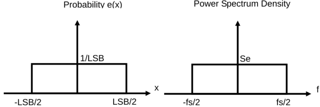
(18) ___________________________________________________________________________Chapter2: Fundamentals of SDM. output of the quantizer and can be plotted versus input signal, as Figure 2.2(b). If the magnitude of input is less than A, its noise error is less than a half of LSB. On the contrast, the noise error greatly grows when the quantizer is overload. Output Overload. LSB/2 Overload. LSB Input. Overload. -LSB/2 Overload. A. Figure 2.2 (a) Transfer curve of ADCs (b) Quantization noise The present trend of ADCs is focused on (a) high resolution, more than 14 bits (b) high speed, more than 100MHz (c) low power. A conflict, however, is likely to exist between each of them when design a real quantizer.. 2.2 Quantization Noise Previous study is focused on static characteristic of ADCs. Next we will focus on its dynamic characteristic. Before that, it is appropriate to use the “white noise approximation” when followed conditions are satisfied [14]: 1. The noise sequence is a sample sequence of a stationary random process. 2. The noise sequence is uncorrelated with the input. 3. The random variables of the noise process are uncorrelated. 4. The probability distribution of the noise process is uniform over the range of quantization noise. Power Spectrum Density. Probability e(x). 1/LSB. Se x. -LSB/2. f. LSB/2. -fs/2. fs/2. Figure 2.3 Probability and power spectral density function of quantization noise __________________________________________________________________ The Design and Implementation of Sigma-Delta Modulator For CMOS Monolithic Temperature Sensors. 6.
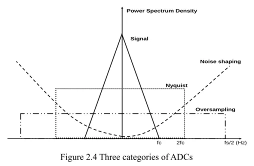
(19) ___________________________________________________________________________Chapter2: Fundamentals of SDM. Therefore the probability density function and the power spectral density function of quantization noise can be sketch in Figure 2.3. Above left figure shows the double side band frequency and leads into frequency domain analysis. On the other words, it is intended as an investigation of dynamic characteristic of ADCs. From Figure 2.3, the total noise power can be estimated by: fs / 2. Pe =. ∫. LSB / 2. Se ( f )df = Se × fs = 2. 2. - fs / 2. ⇒ Se =. 1 2 LSB 2 x dx = ∫ LSB 12 - LSB / 2. (2.2). LSB 2 12 fs. (2.3). Where the fs is the sampling rate and Se is the power spectral density. By the way, owing to an antialiasing filter, input signal of a quantizer is band limited, the bandwidth is referred as fc, the fs must more than double of fc. Because the transfer curve, like Figure 2.2(a), can not be found in frequency domain, we need to define the resolution of ADCs by signal to noise ration (SNR), which is expressed as: SNR = 10 × Log (. Input signal power ) = 6.02 ENOB + 1.76 Output noise power. (2.4) ENOB is the effective number of bits for ADCs. For a given fc, the quantizer can be classified into two groups according to sampling rate, Nyquist-rate and oversampling. Further speaking, oversampling ADCs can be divided into white noise and noise shaping. Three kinds of ADCs mentioned overhead are illustrated in Figure 2.4 and are explained below: 1. Nyquist-rate: the sampling rate is close to double of fc. 2. Oversampling: the sampling rate is more than double of fc. 3. Noise shaping: belong to oversampling group. The probability distribution of the noise process is various over the range of quantization noise. Power Spectrum Density. Signal. Noise shaping. Nyquist. Oversampling. fc. 2fc. fs/2 (Hz). Figure 2.4 Three categories of ADCs __________________________________________________________________ The Design and Implementation of Sigma-Delta Modulator For CMOS Monolithic Temperature Sensors. 7.
(20) ___________________________________________________________________________Chapter2: Fundamentals of SDM. The power spectrum density of white noise is altered from uniform to noise shaping by a noise transform function, NTF. Suppose NTF can be expressed as (1-z-1)m, then we call it m-order sigma-delta modulator (SDM) and the noise shaping can be illustrated in Figure 2.5. It is clear that most of quantization noises are restrained in low frequency and shaped out of band to sharp increase signal to noise ration (SNR) in Nyquist frequency for higher resolution. In order to evaluate its resolution, we estimate the noise power again: NTF ( e. jwTs. wTs ) = 2sin( ) 2. m = 2sin(. πf fs. m ). 2π f ≅ fs. m when f. fs. fc 2 Pe' = ∫ Se2 NTF ( f ) df , Pe' is shaped noise power − fc = Se2 ×. =. π 2 m 22 m +1 fc 2 m +1. × 2m +1. fs 2 m +1. , substitue Se2 by equation (2.2 − 2). LSB 2 π 2m fs − (2 m +1) , M is oversampling ratio = × m ×M 12 2 fc 2 +1. Ideal NTF. Ideal NTF. 8. (2.5). No shaping 1st shaping 2nd shaping 3rd shaping. 1st shaping 2nd shaping 3rd shaping. 0. −50. Magnitude. NTF Gain(dB). 6. 4. −100. −150. −200 2 −250 1. 0.1. 0.2. 0.3. 0.4. Normalized to Fs. −300. 0.5. 0. 0.0001. 0.01. Normalized to Fs. Figure 2.5 The magnitude and gain of NTF __________________________________________________________________ The Design and Implementation of Sigma-Delta Modulator For CMOS Monolithic Temperature Sensors. 8. 0.5.
(21) ___________________________________________________________________________Chapter2: Fundamentals of SDM. For a sinusoidal signal has full scale input, the input signal power is: Pin =. ( A / 2) 2 ( LSB × 2 N −1 ) 2 4 N = = × LSB 2 2 2 8. (2.6). Therefore, the SNR inside the Nyquist bandwidth is derived: SNR = 10 Log ( = 10 Log[. Pin ) = 6.02 ENOB + 1.76 Pe'. 4 N × 12 × (2m + 1) × M 2 m +1 ] 8 × π 2m. = 6.02 N + 1.76 + (2m + 1)10 LogM − 10 Log. π 2m (2.7). 2m + 1. From above equation, it is clear that: 1.. Without oversampling, without SDM structure, thus M=m=0 SNR = 6.02 ENOB + 1.76 = 6.02 N + 1.76. 2.. (2.8). With oversampling, without SDM structure, thus m=0. SNR = 6.02 ENOB + 1.76 = 6.02 N + 1.76 + 10 LogM 3.. (2.9). With oversampling, with SDM structure. SNR = 6.02 ENOB + 1.76 = 6.02 N + 1.76 + (2m + 1)10 LogM − 10 Log. π 2m 2m + 1. (2.10) Where N is the initial bits of ADCs without oversampling or SDM structure, and ENOB is the effective one. We can conclude that, (a) a Nyquist-rate ADC can be express by equation (2.8) and the ENOB is N bits, (b) the higher sampling rate makes the higher resolution, (c) the higher order of SDM makes the higher resolution. Finally, let us devote a table, Table 2.2 and Figure 2.6, to examine the SDM structure. Table 2.2 Summarize the SNR of SDM Structure. SNR. Description. First-order. 6.02N+1.76- 5.17+30LogM. doubling M , increase 9dB. Second-order 6.02N+1.76-12.90+50LogM. doubling M , increase 15dB. Third-order. 6.02N+1.76-21.38+70LogM. doubling M , increase 21dB. m-order. Equation (2.1-10). doubling M , increase (6m+3)dB. We may note, in passing, there are a lot of structures to implement noise shaping topology, SDM is just one of them but is also most feasible one. The reason is that recent CMOS VLSI technology focused on realizing high speed density packed __________________________________________________________________ The Design and Implementation of Sigma-Delta Modulator For CMOS Monolithic Temperature Sensors. 9.
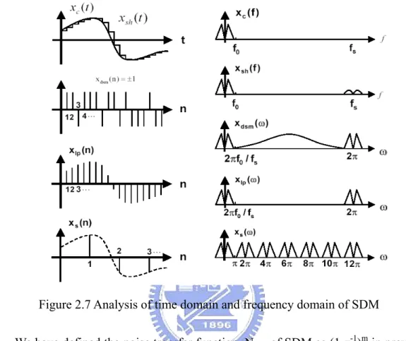
(22) ___________________________________________________________________________Chapter2: Fundamentals of SDM. digital circuits, SDM used only one bit ADC and related analog signal processing circuits are usually have less precision requirements than others.. OSR versus PSNR 98. 86. PSNR (dB). 1−order 2−order 3−order 74. 62. 50. 38 8. 16. 32. 64. 128. Oversampling Ration. Figure 2.6 The SNR of SDM. 2.3 SDM Architecture We shall now look more carefully into the principles of SDM. In practice, recalling Figure 2.1, SDM just one of building blocks of oversampling ADCs. A digital filter and a register are needed to complete fully architecture. From the viewpoint of signal processing, SDM converts continuous analog signals to a sequence digital code, it is like an ADC. The sequence of digital code, however, consists of original signals and shaped quantization noise, a digital filter must remove unnecessary noise to return to original signals. Capitalize Figure 2.7 to realize the correlation between the time domain and the frequency domain of SDM [15]. By contrast, a Nyquist-rate ADC directly maps an analog input into a digital output without further processing. In viewpoint of system level, the latter can effectively generate digital codes, but rarely practical to achieve better than 12 bits resolution without error correction due to mismatching in CMOS process. In order to accomplish high resolution, SDM are widely adopted, for example, DVD-ROM, audio codec, ADSL, cell phone and so on. Briefly speaking, SDM exchange resolution in time for __________________________________________________________________ The Design and Implementation of Sigma-Delta Modulator For CMOS Monolithic Temperature Sensors. 10.
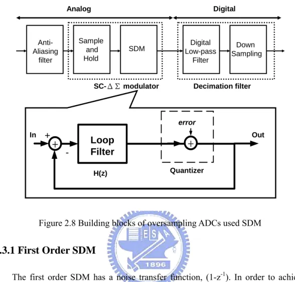
(23) ___________________________________________________________________________Chapter2: Fundamentals of SDM. that in amplitude by combining sampling at well above Nyquist rate with coarse quantizer embedded in order to suppress quantization noise appearing in signal band [16].. Figure 2.7 Analysis of time domain and frequency domain of SDM We have defined the noise transfer function, NTF, of SDM as (1-z-1)m in previous section. The use of feedback illustrated in Figure 2.8 next page to realize NTF of SDM is a familiar structure and has several advantages in CMOS technology, for instant: z Relax the requirements placed on the analog circuitry at the expense of more complicated digital circuitry. z High-resolution analog circuitry is complicated by low power and poor output impedance z Reduced requirements on matching tolerances and amplifier gain. z Simplify the requirements of anti-aliasing filter. z A sample-and-hold is usually not required at the input. Judging from above, SDM provide a robust structure to implement for (a) high resolution ADCs (b) low power system (c) disappointing environment. We need not elaborate on the points of the decimation filter, which are treated much more adequately in references. From the present, we shall confine our attention on various SDM architectures. __________________________________________________________________ The Design and Implementation of Sigma-Delta Modulator For CMOS Monolithic Temperature Sensors. 11.
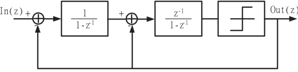
(24) ___________________________________________________________________________Chapter2: Fundamentals of SDM. Analog. Digital. Sample and Hold. AntiAliasing filter. Digital Low-pass Filter. SDM. SC-ΔΣ modulator. Down Sampling. Decimation filter. error In. +. +. -. Loop Filter. +. Out. Quantizer. H(z). Figure 2.8 Building blocks of oversampling ADCs used SDM. 2.3.1 First Order SDM The first order SDM has a noise transfer function, (1-z-1). In order to achieve high resolution, the oversampling ration (OSR), M, can be estimated by Table 2.2. Then it is clear that OSR more than 38 for 8 bits resolution, even more than 96 for 10bits resolution, therefore, the application is narrowed for ultra-low input bandwidth or unfavorable operational status. Refer to Figure 2.8, the loop filter has transfer function, H(z). The output can be written in term of input and quantization error as: ∵ Out ( z ) = E ( z ) + H ( z ) ⎡⎣ In ( z ) −Out ( z ) ⎤⎦ ∴Out ( z ) = STF ( z ) In ( z ) + NTF ( z ) E ( z ) H ( z )=. A( z ) B( z). H (z) A( z ) STF ( z ) = = 1+ H ( z ) A ( z ) + B ( z ) N TF ( z ) =. (2.11). B( z) 1 = A( z )+ B ( z ) 1+ H ( z ). (2.12). __________________________________________________________________ The Design and Implementation of Sigma-Delta Modulator For CMOS Monolithic Temperature Sensors. 12.
(25) ___________________________________________________________________________Chapter2: Fundamentals of SDM. Where NTF and STF is noise and signal transfer function, respectively. We can observe that, the zeros of the NTF are equal to the poles of the H(z). Therefore, in order to curtail noise power, maintain the H(z) is large and NTF(z) is small in the frequency band of interest. For instance, we can choose H(z) is a low-pass filter and NTF(z) is a high-pass filter to construct a low-pass sigma-delta modulator (LP-SDM). Toward that, the simplest case of H(z) is (z-1)-1, which is a discrete-time integrator, so the resulting output is : −1. Out ( z ) = z In ( z ) + (1 − z. −1. )E(z). (2.13) This shows that the output is delayed by one sample period. Ideally, a quantizer does not introduce amplitude distortion and has a linear phase characteristics [17].. Figure 2.9 A first order SDM. 2.3.2 Second Order SDM The second order SDM is widely used, and Figure 2.10 shows the building blocks, and the output is: −1. Out ( z ) = z In ( z ) + (1 − z. −1 2. ) E(z). (2.14) Note that, compared with first order SDM, the second order SDM provides more quantization noise suppression over the low frequency band, thus more noise power outside the input bandwidth [18]. Suppose OSR is 64, this structure can be a 12 bit ADC due to equation (2.10).. Figure 2.10 A second order SDM __________________________________________________________________ The Design and Implementation of Sigma-Delta Modulator For CMOS Monolithic Temperature Sensors. 13.
(26) ___________________________________________________________________________Chapter2: Fundamentals of SDM. 2.3.3 Higher Order SDM A high order SDM is often defined as a SDM with the number of order higher than three. It is obvious that higher order SDM requires lower OSR to achieve the same SNR, for instance, it can be a 13 bit ADC when OSR is 32. The order, however, is less than six is compatible in CMOS technology because of instability and mismatching problems. Stability of SDM is defined that as one in which the input to the quantizer remains bounded such that the quantization does not become overloaded. In fact, the stability of higher-order modulator is not well understood as they include a highly nonlinear element, especially embedded low-bit quantizers. A rule of thumb for a stable SDM is expressed in equation (2.15), but it has little rigorous justification. A useful stable criterion is proposed by [19]. NTF ( e jωT ) ≤ 1.5 for 0 ≤ ω ≤ π. (2.15) High order SDM is divided into signal-stage and multi-stage structures [20]. Single-stage structure contains Feed-forward (FF) modulator, Multiple-feedback (MF) modulator and others. Figure 2.11(a) and Figure 2.11(b) gives an example of them diagrammatically. Multi-stage structure (MASH) uses several stages instead of a single loop to reduce the quantization noise of the coarse quantizer. A second stage followed by a first order SDM shown in Figure 2.11(c) is used usually because it is insensitive to circuit performance.. Figure 2.11 Higher order SDM __________________________________________________________________ The Design and Implementation of Sigma-Delta Modulator For CMOS Monolithic Temperature Sensors. 14.
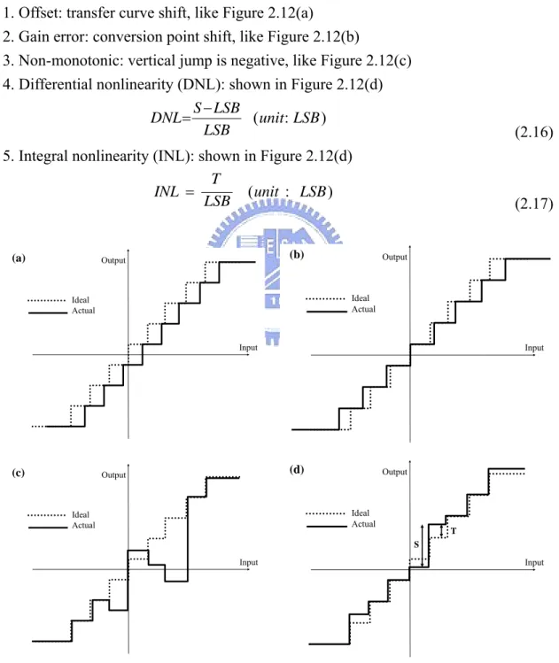
(27) ___________________________________________________________________________Chapter2: Fundamentals of SDM. 2.4 Performance Metrics In practice, transfer characteristics are different from Figure 2.2 and Figure 2.4 because imperfections in a practical implementation. Performance metrics are used to describe the deviation are fall into static and dynamic categories which are main subject here. Static performance metrics: 1. Offset: transfer curve shift, like Figure 2.12(a) 2. Gain error: conversion point shift, like Figure 2.12(b) 3. Non-monotonic: vertical jump is negative, like Figure 2.12(c) 4. Differential nonlinearity (DNL): shown in Figure 2.12(d) S − LSB DNL = ( unit : LSB ) LSB. (2.16). 5. Integral nonlinearity (INL): shown in Figure 2.12(d) T INL = ( unit : LSB ) LSB. (2.17). (a). (b). Output. Output. Ideal Actual. Ideal Actual. Input. Input. (c). (d). Output. Output. Ideal Actual. Ideal Actual. T S Input. Input. Figure 2.12 Static performance metrics. __________________________________________________________________ The Design and Implementation of Sigma-Delta Modulator For CMOS Monolithic Temperature Sensors. 15.
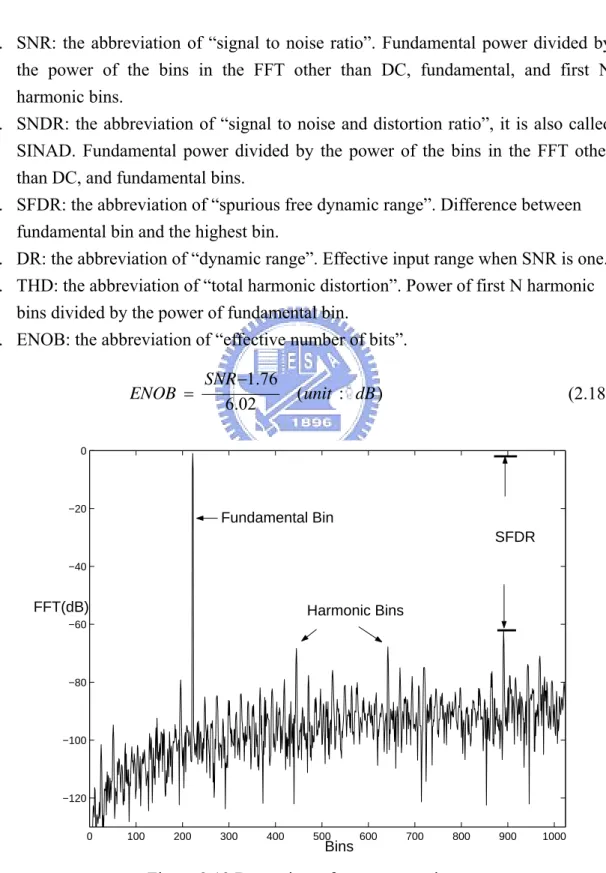
(28) ___________________________________________________________________________Chapter2: Fundamentals of SDM. Dynamic performance metrics is measured with a low-noise full scale sine wave to the ADC, performed continuous conversions on the input signal, collect the conversion results, performed a Discrete Fourier Transform (DFT) to map into Fast Fourier Transform (FFT) spectrum. Some of these are listed below and the unit is “dB”. 1. SNR: the abbreviation of “signal to noise ratio”. Fundamental power divided by the power of the bins in the FFT other than DC, fundamental, and first N harmonic bins. 2. SNDR: the abbreviation of “signal to noise and distortion ratio”, it is also called SINAD. Fundamental power divided by the power of the bins in the FFT other than DC, and fundamental bins. 3. SFDR: the abbreviation of “spurious free dynamic range”. Difference between fundamental bin and the highest bin. 4. DR: the abbreviation of “dynamic range”. Effective input range when SNR is one. 5. THD: the abbreviation of “total harmonic distortion”. Power of first N harmonic bins divided by the power of fundamental bin. 6. ENOB: the abbreviation of “effective number of bits”. ENOB =. SNR −1.76 6.02. ( unit : dB ). (2.18). 0. −20. Fundamental Bin SFDR. −40. FFT(dB). Harmonic Bins. −60. −80. −100. −120. 0. 100. 200. 300. 400. 500. Bins. 600. 700. 800. 900. 1000. Figure 2.13 Dynamic performance metrics __________________________________________________________________ The Design and Implementation of Sigma-Delta Modulator For CMOS Monolithic Temperature Sensors. 16.
(29) _____________________________________________________ __________Chapter3: System Level Design Considerations. Chapter3 System Level Design Considerations ___________________________________________________________ This chapter discusses defects of actual SDM caused by thermal noise, OPAMP finite gain, clock jitter, and so on. Several mathematical methods are proposes to estimate the curtailed Peak SNR of SDM. In addition to this, design issues to overcome high temperature impact and leakage current are discussed in section 3.2. Both of them are major problems for proposed SDM design. In the end of this chapter, several approaches to overcome above limitation are proposed and the detail mechanisms of such improvement are discussed.. ___________________________________________________________ 3.1 Limitations A SDM used noise shaping topology gives rise to an increase of in-band SNR, and the Peak SNR can be obtained by equation (2.7), and the Figure 2.5 shows the quantization noise is suppressed in low frequency and increased in high frequency. However, the NTF accomplished by switched-capacitor technology with OPAMP have two fundamental limitations, namely non-zero turn-on resistances of switches and non-ideal amplifier. The former generate the thermal noise, the latter contains finite gain, finite bandwidth, and slew rate.. Figure 3.1 A SC integrator A switched-capacitor integrator (SCI) is popularly adopted to accomplish NTF in SDM structures. Figure 3.1 shows a SC integrator which has transfer function: H (z) =. C1 z −1 z −1 × = × Ratio C2 1− z − 1 1− z − 1. (3.1). __________________________________________________________________ The Design and Implementation of Sigma-Delta Modulator For CMOS Monolithic Temperature Sensors. 17.
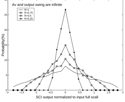
(30) _____________________________________________________ __________Chapter3: System Level Design Considerations. Above equation is satisfied when DC gain is infinite, but the finite gain of this amplifier is considered now, then equation 3.1 is altered as: H (z) = R ×. z −1. 1 (1 + R ) Av. α = 1+. (3.2). α − β z −1 1 Av. β = 1+. Where Av is open loop gain and R is the capacitor ratio of SCI. So the first order SDM has: Rz − 1 α − β z −1 (3-3) S TF = N = & −1 −1 TF α −(β − R ) z. α −(β − R ) z. Then, NTF can be calculated as equation below and illustrated in Figure 3.2: 1 (2+ R ) R Av ( 0.5 fs ) = = 1+ 1 1 ( 2− R )+ (2+ R ) ( 2− R )+ (2+ R ) Av Av 2+. N. TF. N T F ( dc ) =. (3.4). 1 1 R & N TF ( 3 dB ) ≅ 2 π Av + 1 Av + 1. (3-5). NTF Gain(dB). Effect of Integrator Leakage 0 −10 −20 −30 −40 −50 −60 −70 −80 −90 −100. R=1,Av=50dB R=1,Av=60dB R=1,Av=70dB R=1,Av=80dB R=1,Av=infinite. −6. 10. −5. 10. −4. −3. 10. 10. −2. 10. −1. 10. Normalized to Fs Effect of Integrator Leakage. NTF Gain(dB). 0. −20. −40. R=2/3,Av=80dB R=4/3,Av=80dB R=8/3,Av=80dB R=16/3,Av=80dB R=1,Av=infinite. −60. −80. −100 −6. 10. −5. 10. −4. −3. 10. 10. −2. 10. −1. 10. Normalized to Fs Figure 3.2 Effects of leakage in the SCI __________________________________________________________________ The Design and Implementation of Sigma-Delta Modulator For CMOS Monolithic Temperature Sensors. 18.
(31) _____________________________________________________ __________Chapter3: System Level Design Considerations. If the order of SDM and OSR are simultaneously invoked into integrator leakage, equation (2.5) can be expressed [21]: ⎫⎪ LSB 2 ⎧⎪ µ 2π 2 m−2 m ' π 2m ⎬ ×⎨ + Pe ≅ 12 ⎪⎩ (2 m −1) M 2 m−1 (2 m +1) M 2 m+1 ⎪⎭. (3.6). µ = R / Av. This error degrades the SNR and contributes the noise floor in-band. Figure 3.2 indicates us that the higher OPAMP gain and the higher capacitor ratio, the more quantization noise are repressed at low frequency. Nevertheless, the feedback factor has its ceiling to avoid two effects: (1) Overload of quantizers: Because limited input range of quantizers. Figure 3.3 shows the probability distortion of the integrators outputs, it implies that dynamic range is required more times of full scale input for larger ratio to ensure quantization noise is less than a half of LSB. This requirement restricts the input range of modulators when input range of quantizers is confined. 30. Av and output swing are infinite R=1 R=0.75 R=0.5 R=0.25. 25. Probability(%). 20. 15. 10. 5. 0 −2. −1.5. −1. −0.5. 0. 0.5. 1. 1.5. 2. SCI output normalized to input full scall. Figure 3.3 Comparison of SCI output probability densities for different feedback factor (2) SCI distortion: This distortion is caused by the limited output range of OPAMP, as sketched in Figure 3.4, warps SCI output waveform which reflects the sum of input signal and feedback signal and will bring about inaccurate bit-steam produced by quantizers. The higher resolution of quantizers, the worse SNR exists __________________________________________________________________ The Design and Implementation of Sigma-Delta Modulator For CMOS Monolithic Temperature Sensors. 19.
(32) _____________________________________________________ __________Chapter3: System Level Design Considerations. when SCI distortion happened.. SCI output waveform Normalized to input full scall. SCI output waveform Normalized to input full scall. Time Domain Analysis 1. 0.5. 0. −0.5. −1. 0. 100. 200. 300. 400. 500. Ts. 600. 700. 800. 900. 1000. 600. 700. 800. 900. 1000. 1. upper output range 0.5. 0. −0.5. lower output range −1. 0. 100. 200. 300. 400. 500. TS. Figure 3.4 Simulated integrator distortions The Z transform is good to describe SC integrator efficiently, the transform function indicates the stable states as well as low clock rate. Unfortunately, the final sample and setting voltage have deviation between the ideal cases calculated by equation (3.1) due to limited period and RC time constant, this error is called as “incomplete setting noise”. A transient model needs to be established for an accurately designed SDM. For simplicity, we assume a single-pole and limited output current model for OPAMP in the SC integrator. (a). Va. C1. Vo. C2. Cp. gmVa. ro. CL. Vo(t). (b). Incomplete setting error Va(Ts/2). Vo,n-1 Ts/2. to Integration phase. Sampling phase Saturation. Time. Sampling phase. linear. Figure 3.5 (a) Equivalent model for integration mode (b) Time evolution of vo __________________________________________________________________ The Design and Implementation of Sigma-Delta Modulator For CMOS Monolithic Temperature Sensors. 20.
(33) _____________________________________________________ __________Chapter3: System Level Design Considerations. An equivalent circuit during the integration phase is shown in Figure 3.5(a). Owing to the fact that C1 samples the input voltage and a feedback path provided by C2 and OPAMP, the vo jump in the opposite direction to the final increase, and a similar evolution occurs in the input node whose va experiences a jump in the instant in which switches S1 and S2 are just closed [21]. Depending on the value of va, we will distinguish two operational modes, (a) Linear: if │gmva│< Io, (b) Saturation: if │gmva│> Io, where Io is the maximum output current of OPAMP. Suppose t=0 at the end of sample phase, and t=to at the end of saturation mode, like illustrated in Figure 3.5(b). The output voltage is a function of time and we will discuss it in detail at next page and study the effect of this kind of voltage error by some equations. The initial value of va(t=0) and vo(t=0) can be obtained by charge conservation: v a ( t = 0 ) = v ai =. − C1. vi C C C1 + C p + 2 L C2 + C L. (3.7). C2 v o ( t = 0 ) = v oi = v o [( n − 1) Ts ] + v C 2 + C L ai. (3.8). Capitalize the RC time constant to derive vo(t), when linear mode: ⎡ ⎤ v o ( t ) = v o ( t = ∞ ) + ⎢⎣ v oi − v o ( t = ∞ ) ⎥⎦ e C v [( n −1) Ts ] + 1 vi C2 vo ( t = ∞ ) = C + Cp 1 1+ (1 + 1 ) Av C2 R e q = ( g o + gm ×. C2. C1 + C 2 + C p. ,. )−1. −t R e q C eq. (3.9). Av = gm ro. &. C eq = C L +. ( C1 + C p ) C 2 C1 + C p + C 2. At saturation mode, for go is much smaller than one, the va(t) is expressed by equation (3.7) and to can be calculated when this equation is equal to Io/gm, so: va (t ) =. t0 =. − C1 C2C L. vi +. C1 + C p + C2 + CL. C1 CL −C + (1 + ) vi gm Io C2. C2 Io × sgn( vi ) × t C eq C1 + C p + C 2. & C = C 1 + C p + C L (1 +. C1 + C p ) C2. (3.10) (3.11). For t > to, the SC integrator is operating at linear mode, we can get: ⎡ ⎤ v o ( t ) = v o ( t = ∞ ) + ⎢⎣ v o ( t = t o ) − v o ( t = ∞ ) ⎥⎦ e vo ( t = t o ) = vo [( n −1) Ts ] +. − ( t − to ) R e q C eq. − C1 Io × sgn( vi ) vi + × to C2C L C eq C1 + C p + C2 + CL − ( t − to ) R e q C eq. (3.12). (3.13). vo ( t = ∞ ) ⎡ v (t =∞ ) ⎤ e + ⎢ v a ( t = to ) − o − − Av ⎦⎥ Av ⎣ __________________________________________________________________ va ( t ) =. The Design and Implementation of Sigma-Delta Modulator For CMOS Monolithic Temperature Sensors. 21.
(34) _____________________________________________________ __________Chapter3: System Level Design Considerations. The time constant in equation (3.12) is the same with equation (3.9). Combing equation (3.9) and (3.12), we can obtain the value in the end of integration phase. Output voltage happen to another drop because va tend to analog ground during next sampling phase and the voltage stored in C2 keeps constant, as shown in Figure 3.5(b). General speaking, CL (Cp) is much smaller than C2 (C1), therefore: C1 = R C2. &. Av >> 1. v ai = − vi , v oi = v o [( n −1) Ts ] − vi , v o ( t = ∞ ) = v o [( n − 1) Ts ] + R × vi R e q C eq = C1 / gm =τ C C / C eq 1+ R t o = 1 vi −τ = 1 vi −τ = vi −τ Io Io / C eq SR. When linear mode:. −t. v o ( t ) = v o [( n − 1) Ts ] + R × vi − (1 + R ) vi × e. τ. (3.14). When saturation mode: ⎧⎪ v o ( t ) = v o [( n −1) Ts ] − vi + SR × t − ( t − to ) ⎨ ⎪⎩ v o ( t ) = v o [( n −1) Ts ] + R × vi − [(1 + R ) vi − SR × t o ] e τ. t ≤ to t ≥ to. (3.15). Above equations imply that, some error introduced in integrator output can be seen as the error term of SC integrator. This will make up distortion and harmonics at the modulator output, and this error exits a dependency between the leakage of the integrator, slew rate and its input voltage. Another noise source is thermal noise, which contribute principally to the overall thermal noise power are the non-zero turn-on resistance of switches, both sampling and integration phase, and the input-referred OPAMP. The total power of thermal noises is proposed by [21]. Pth ≅. kT kT 1 + ( + gm R on ) 4 M C1 2 M ( C1 + C p ) 3. (3.16). Where k is the Boltzman’s constant and its value is 1.38╳10-23, T is absolute temperature and Ron is the turn-on resistance of switches. Note that equation (3.16) should be multiplied by two when referred to fully-differential structures. For time domain simulation, thermal noise can be modeled as a noise source with n(t) denotes a Gaussian random process with unit standard deviation [22], which is: Vth =. kT kT 1 + ( + gm R on ) × n ( t ) 4 M C 1 2 M ( C1 + C p ) 3. (3.17). __________________________________________________________________ The Design and Implementation of Sigma-Delta Modulator For CMOS Monolithic Temperature Sensors. 22.
(35) _____________________________________________________ __________Chapter3: System Level Design Considerations. Clock jitter refers to the temporal variation of the clock period at a given point on the chip, thus the clock period can reduce or expand on a cycle-by-cycle basis. Jitter is a zero-men random variable [23]. Once the analog signal has been sampled, the SC circuit is a sampled-data system where variations of the clock period have no effect on the circuit performance. This also means that effect of clock jitter on a SDM is independent of the stricture and the order of the modulator. As a result, a non-uniform sampling time sequence produces an error which increases total error at x ( t + D )- x ( t ) d the quantizer output. ≅ x (t ) D. dt. if x ( t ) = Ain × sin( 2 π fin × t ) ⇒. d x ( t ) = 2 π fin [ Ain × cos( 2 π fin × t ) ] dt. ∴ x ( t + D ) = x ( t ) + D × 2 π fin [ Ain × cos( 2 π fin × t ) ] = input signal + error sorce (V jitter ) ⇒ P jitter =. Ain 2 ( 2 π fin ) 2 2. ⇒ Vjitter =. Ain 2 π fin × d ( t ) 2. (3.18). (3-19) Here, we suppose D is a Gaussian random process with standard deviation d [22]. A behavior model established in MATLAB with a sub-circuit, shown in Figure 3.6 and Figure 3.7, can be used to determine the sensitivity to analog sub-circuits, and the circuit level specifications are decided. The set of blocks takes in account of imperfection previous study.. Figure 3.6 A behavior model implemented in MATLAB __________________________________________________________________ The Design and Implementation of Sigma-Delta Modulator For CMOS Monolithic Temperature Sensors. 23.
(36) _____________________________________________________ __________Chapter3: System Level Design Considerations. Figure 3.7 The sub-circuit of loop filter It should be concluded, from what has been said above, the Peak SNR is reduced by: z OPAMP open loop gain, equation (3.6). z OPAMP slew rate and BW, equation (3.15). z Thermal noise of switches and OPAMP, equation (3.16). z Clock jitter, equation (3.18). z Others: OPAMP saturation voltages, Capacitors ratio.. 3.2 Higher Temperature Issues Current commercial CMOS technologies can be used without any process modifications to design circuits useful up to 250oC [24]. However, thermal effects on small signal parameters of CMOS are studied necessarily to figure out the design tradeoffs and considerations limitation for analog circuits. Table 3.1 lists some parameters with level 2 model [25], it is evident that the drain current have strong dependency on temperature, furthermore all of small signal models as transconductance and output resistance, are based on the amount of drain current. We may, therefore, reasonably conclude that the relationship between these parameters and temperature is quite close. Direct deriving correlations, however, bring about complex results and inefficiency on circuit design. Fortunately, some effectives equations proposed in [24] are present along with the temperature dependencies of key design parameters and represent sufficient information for first-order hand analysis prior to CAD design.. __________________________________________________________________ The Design and Implementation of Sigma-Delta Modulator For CMOS Monolithic Temperature Sensors. 24.
(37) _____________________________________________________ __________Chapter3: System Level Design Considerations. Table 3.1 Some parameters of NMOS with level 2 model Parameter. Equation. Drain current. ID =. µ Cox W 2. L. ×(VGS −VT )2 ×(1+ λVDS ). 2 kT N sub ln VT =VFB +φ + K1 (φ −VBS )0.5 ←φ = q ni. Threshold voltage Intrinsic carrier concentration. 15. ni = 7.785 × 10. Band gap of silicon. Eg =1.17 −. ×T. 3 2. ×e. − Eg 2 kT. 4.73×10⁻⁴ 2 T T + 636. µ is effective mobility ,ϕ is surface potential , K 1 is substrate effect coefficient. The effects of temperature on large signal parameters of the MOSFET are discussed first. Recalling the drain current, wherein threshold voltage and effective mobility are critical points. Whether both of them are analytical quantity, two good approximations can describe the temperature dependency, thus: Vth ( T ) = α T + β. µ ( T ) = µ ( To ) × (. (3.20) (3.21). T γ ) To. Where T is absolute temperature, (α, β, γ) are parameters depend on processing. Then we can estimate the Zero-Temperature-Coefficient (ZTC) bias points for saturation region, at which the drain current exhibits minimum temperature sensitivity, it is possible to write: ∂I D ∂ I D ∂ Vth ∂I D ∂µ ∂T. =. =. ∂ Vth. ∂T. +. ∂µ. ∂T. ∂I D ∂I γµ ×α + D × ∂ Vth ∂µ T. ⎛ −2α γ ⎞ = I D ×⎜ + ⎟ ⎝ Vgs − Vth T ⎠ if. ∂I D 2α = 0 ⇒ Vgs sat = Vth + T γ ∂T. (3.22). Another ZTC bias point over the range [T1, T2] is addressed in [24], that is: Vgs sat = β −. ( T1 + T2 ) α 6. (3.23). In 0.25μm CMOS technology, (α, β, γ) = (-0.9m, 800m, -1.5) and (+0.88m, -1124m, -1.5) for NMOS and PMOS respectively. Using equation (3.20), (3.22) and (3.23), the ZTC bias point for a NMOS during temperature [300k, 500k] is about 920mv. If we use HSPICE to fide out this ZTC bias point, shown in Figure 3.8, its value is 897mv. __________________________________________________________________ The Design and Implementation of Sigma-Delta Modulator For CMOS Monolithic Temperature Sensors. 25.
(38) _____________________________________________________ __________Chapter3: System Level Design Considerations. A similar result is exhibits in triode region can be expressed as: Vgs triode = β + **. ( T1 + T2 ) α 6. ztc. (3.24). **. 6m. 5.5m. 5m. 4.5m. Currents (lin). 4m. 3.5m. 3m. 2.5m. 2m. 1.5m. 1m. 500u. ZTC. bias. points. 0. 1.2. 1. 800m. 600m. 1.4. 1.6. 1.8. 400m Voltage. X. (lin). (VOLTS). Figure 3.8 ZTC bias points for NMOS (14μm/0.7μm) in 0.25μm process By the way, retuning to equations (3.20) and (3.21), the threshold voltage decreases with down scaling, the mobility have no effect with down scaling, and the ration of n to p inversion layer mobility μn(T)/μp(T) remains approximately constant between 25oC and 250oC [26]. Let us consider small signal models right now. Most important two parameters are transconductance and output resistance, which determine the gain and bandwidth of many circuits. It is easy to write that: gm =. 2 I D (T ). Vgs − Vth ( T ). ∂ gm gm γ ∂ I D 1 = × ( + ) ∂T ∂T I D 2 T rds = ∂ rds ∂T. (3.25). 1. λ ID =. ∂I D ∂T. ×. − rds ID. (3.26). __________________________________________________________________ The Design and Implementation of Sigma-Delta Modulator For CMOS Monolithic Temperature Sensors. 26.
(39) _____________________________________________________ __________Chapter3: System Level Design Considerations. Previous equations imply that the minimum variation of transconductance and output resistance occur at ZTC bias point. So, in order to maintain the same characteristic during temperature rise, bias at ZTC is the best choice, below are simulation results:. Figure 3.9 Id, gm, gds characteristics for ZTC, ZTC+0.2v, ZTC+0.6v If the temperature is higher than 250oC, sharp increases in the output conductance and body effect transconductance have consistently been observed [27], it has been determined that diffusion leakage current. The various leakage currents comprise the following: 1. The drain and source to body junctions’ bottom wall component, Ib(T), which is proportion to W and D, shown in Figure 3.10. 2. The drain and source to body junctions’ sidewall wall component, Isw(T), which is proportion to W and X, shown in Figure 3.10. 3. The inversion layer to body junctions component, Ich(T), which is proportion to the W and L, shown in Figure 3.10. __________________________________________________________________ The Design and Implementation of Sigma-Delta Modulator For CMOS Monolithic Temperature Sensors. 27.
(40) _____________________________________________________ __________Chapter3: System Level Design Considerations. D Gate Drain. Source L Isw. Isw. X. W. Ich Ib. Ib. Body. Figure 3.10 Leakage current components Leakage current, in particular, can be a significant source of impairment and is worthy of a more detail review. The ideal P-N diode current is described by: 2. I D iode = Aqn i K D ( e. qVF kT. − 1). A is the area of leaky diodes. If this diode is operated under strong reverse, it can be 2 reduced as: I D iode = − Aqn i K D. In addition to this, there is reverse bias current due to generation-recombination events within the depleted region, which is: I G R = − Aqn i K G R. So, the total leakage current in the reverse bias as shown [12]: 2 I L = − Aqn i K D − Aqn i K G R. (3.27) Figure 3.11 indicates that, the leaky diodes are sinks and sours at the drain or source node of NMOS and PMOS respectively. Although, we can use equation (3.27) to calculate leakage current, but the exactly amount is difficult to predict and hard to avoid. Design a compensation circuit is more effective to restrain thermal problems.. IL. IL. IL. IL. IL. IL. Figure 3.11 The leaky junction diodes are explicitly shown in CMOS __________________________________________________________________ The Design and Implementation of Sigma-Delta Modulator For CMOS Monolithic Temperature Sensors. 28.
(41) _____________________________________________________ __________Chapter3: System Level Design Considerations. The principle of compensation circuits is algebraic sum of all leakage current be zero at any given node. If one was not this case, net leakage current would flow into or out of this node, thus forcing an increase or decrease in drain current of adjacent transistors, which result in voltage shift from bias points and performance degrade. To this point, adding diodes or complementary structure are approaches to reduce leakage current, as sketches below. Compensation Diode. Voltage dividing string. Transmission gates. Figure 3.12 Compensation circuits for leakage current We should note that transmission gates, show in Figure 3.12, this structure is popular in the switches-capacitor system to be a switch. The leakage current is not matched all the time and keeps almost constant for any given node, thereby charging or discharging loading capacitors, so that setting or holding error as a result. Increasing clock rate, which can decrease the charging or discharging time, is one way to solve this problem. From previous study, we can make a conclusion below to minimize leakage current in high temperature environment: z Small diffusion area z Low leakage switches z Compensation devices, like diodes z Matching leakage area z Bias at ZTC points z External capacitors to increase the time constant z High clock rate. __________________________________________________________________ The Design and Implementation of Sigma-Delta Modulator For CMOS Monolithic Temperature Sensors. 29.
(42) _______________________________________________________________________ __Chapter4: Implementation of SDM. Chapter4 Implementation of Proposed Sigma Delta Modulator ___________________________________________________________ A prototype of proposed sigma delta modulation has been fabricated in TSMC 0.25μm single-ploy five-metal CMOS process. The circuitry is operating at a supply voltage of 3.3 volt. The design issues for this prototype in circuitry, transistors and physical levels are thoroughly discussed in this chapter. The whole circuitry blocks are described in Section 4.1. In Section 4.2 the sub-circuitry of each component is presented, which includes OPAMP, comparator, switch capacitors, integrator, feedback DAC, and output buffers. In Section 4.3, the final physical design of proposed SDM prototype is then described.. ___________________________________________________________ 4.1 Circuit Level Design The detail schematic design and system considerations have been present in earlier this thesis. Implementation of these principles to an actually monolithic chip is our objective here. Let us recall all of building blocks of SDM, they are a loop filter, a quantizer, the feedback path and an adder. We should notice that a loop filter and an adder can be carried out by a differential SC integrator, and another advantage of this is a sample and hold circuit call be omitted. In addition to this, a one-bit ADC is used be to be a quantizer for SDM. Therefore the SDM can be divided into three parts, which consist of sub-circuits, and we can summarize them in Table 4.1 below. Table 4.1 Organization of SDM Schematic. Building Block. Sub-circuit. Section. Adder. OPAMP. 4.2.1. Loop Filter. Differentia SC Integrator. Switches & Capacitors. 4.2.3. Quantizer. 1 bit ADC. Comparator. 4..2.2. Feedback Path. 1 bit DAC. Feedback DAC. 4.2.5. Output buffer. 4.2.6. A fully experimental SDM circuit is shown in Figure 4.1 at next page, input and output signal are illustrated simultaneously. The key point I wish to emphasize is that, output buffers are required due to parasitic package capacitors. __________________________________________________________________ The Design and Implementation of Sigma-Delta Modulator For CMOS Monolithic Temperature Sensors. 30.
(43) _______________________________________________________________________ __Chapter4: Implementation of SDM. S1. S2. S3. S4. C1 S1. S2. S3. S5. C2. Feedback DAC. OPAMP. Comparator. Output buffer. Cos S4. S5. C2 Output buffer. Feedback DAC. S/B PACKAGE. Input signal, Power Supply, Control voltages. SDM output. Figure 4.1 Circuit level of SDM Two topologies, switched-capacitor (SC) and correlated double sampling (CDS), are invoked, so there are ten switches and six capacitors are employed. We list device ration of switches and capacitors sizes in Table 4.2 first, the detail design considerations of them will be discussed at section 4.2.3 and 4.2.4 later. Table 4.2 Switches and comparators information Component. S1. Size 20μm/0.36μm. Type. NMOS. During Φ1d. S1. 20μm/0.36μm. PMOS. Φ2d. S2. 4μm/0.36μm. NMOS. Φ2d. S3. 4μm/0.36μm. NMOS. Φ1. S4. 20μm/0.36μm. NMOS. Φ2. S5. 20μm/0.36μm. NMOS. Φ1. C1. 0.4pF. MIM. Always. C2. 0.5pF. MIM. Always. Cos. 0.5pF. MIM. Always. __________________________________________________________________ The Design and Implementation of Sigma-Delta Modulator For CMOS Monolithic Temperature Sensors. 31.
(44) _______________________________________________________________________ __Chapter4: Implementation of SDM. Above table also lists operational period of switches in order to (a) sample input and add feedback signal (b) use CDS technology (c) avoid charge injection. In other words, Figure 4.1 is controlled by two phase, non-overlapping clocks, Φ1 andΦ2, a delayed clock phase Φ1d andΦ2d. A timing diagram illustrating these clock signals are shown in Figure 4.2.In practice, these clocks are generated by external circuit and will be described in Chapter 5. By the way, all of circuit level design and transistors level design are using the CAD simulation tool, HSPICE.. φ1. φ1d. φ2. φ2d time Figure 4.2 A timing diagram illustrating clock signals. 4.2 Transistors Level Design This section described the elaboration of sub-circuits that will be used to realize an actual integrated circuit, which covers an operational amplifier (OPAMP), a comparator, switches and capacitors, and feedback path. The simulation results and device ratios are given at each section.. 4.2.1 Differential OPAMP Utilizing switched-capacitor technology and an operational amplifier (OPAMP) to realize a loop filter in a SDM is a common circuitry for high speed and low power __________________________________________________________________ The Design and Implementation of Sigma-Delta Modulator For CMOS Monolithic Temperature Sensors. 32.
(45) _______________________________________________________________________ __Chapter4: Implementation of SDM. applications. It is clearly that, however, the performance of this loop filter dominates dynamic specifications of a SDM. Designing a high performance OPAMP is the main purpose in this section. In addition to a main circuit, a bias circuit and a common mode feedback circuit (CMFB) will be discussed. VDD. M17. M19. M22. M3. M4. M5. M6. Vb1. M18. M20. M23. Vo1. Vb2. CL. Vi1. Vcm. Vi2 M1. Vo2 M11 CL. M2. M12. M13. Vb3. M24. M7. M8. Vcmc. Vf. Vb4. Iref. M21. M16. M9. M10. M14. M15. VSS. Figure 4.3 Fully differential OPAMP Figure 4.3 shows the fully differential OPAMP including its bias circuit and CMFB. The OPAMP, which is a folded cascade amplifier, was chosen for its large dc gain and ability to drive capacitive loads [12]. The bias circuit supplies several internal bias voltages except Vcm. The CMFB determine the output common mode voltage and control it to be a specified voltage [15]. The OPAMP circuit consists of eleven transistors, from M1 to M10 and M16. The first stage including M1, M2, and M16; the remainders are second stage. It must be noted that the drain current of M16 determines the slew rate of this amplifier. Added to this, the drain current of M3 (or M4) should be more than M16 to avoid operating failed during slewing. By Naming the drain current of M3 and M16 is “Iss” and “Ir” respectively, the drain currents of M7 to M10, which are active loads, can be represented as Ir minus Iss. This shows that the device ratios of active loads don’t affect the quantity of current, but affect the voltage gain sufficiently. Briefly speaking, high output resistance is the critical issue to design these four transistors. And then __________________________________________________________________ The Design and Implementation of Sigma-Delta Modulator For CMOS Monolithic Temperature Sensors. 33.
(46) _______________________________________________________________________ __Chapter4: Implementation of SDM. higher output resistance, higher DC gain. From above discussions, we obtain the following results: If (. W ) =S i L i. If Vgs - Vth =Vov S16 =. 2× Iss. (4.1). µ nCoxVov 2. S 3,4,5,6 =. 2× Ir. µ nCoxVov 2. S 7,8,9,10 =. 2× ( Ir − 0.5 Iss ) µ nCoxVov 2. (4.2) (4.3). The device ratio of M1 and M2 are another critical issue for high DC gain. By the way, the unit-gain frequency (Fu) is also dependent on their sizes. It can be found that: Fu ≅. gm1,2 ⇒ gm1,2 = 2π FuCL 2π×CL. gm1,22 S1,2 = µnCoxIss. (4.4). The overall gain of this amplifier can be derived from Figure 4.4, and the detail procedure is given: R = ro7 + (1 + gm7ro7 )ro9 ≅ gm7ro7ro9 r RB= o5 1+gm5ro5 RA=ro3 // ro1 gm i1= 1×Vid 2 i=i1×. RA RA+RB. −Vo =−i×Rout 2 Rout =R// gm5ro5RA ∴ Gain =. gm1( gm7ro7ro9 // gm5ro5RA) r 1+( go1+go3)( o5 ) 1+gm5ro5. (4.5). __________________________________________________________________ The Design and Implementation of Sigma-Delta Modulator For CMOS Monolithic Temperature Sensors. 34.
(47) _______________________________________________________________________ __Chapter4: Implementation of SDM. Vb1. i1 RA Vid/2. RB Vb2 i R. -Vo/2 Rout. Vb3. Vcmc. Figure 4.4 Small signal equivalent circuit of OPAMP The bias circuit contains eight transistors, from M17 to M24. Its outputs are four independent voltage sources to drive OPAMP operating at active mode. Strictly speaking, M22 and M3 is a current mirror pair. Compared with the drain current of M3, the quantity of Vb1 is not the key point in design. In other words, the amount of current and minimum output voltage should be considered prior to Vb1 when design the size of M22 in order to ensure it could be a current mirror source. A similar result could be found in M21.On the other hand, using two skills for higher output swing [28]. First is minimizing the size of M18, second is connecting the gates of M23 and the source of M20. Figure 4.5 shows the results diagrammatically.. Traditional Vb1. Modified Vb1. S. Vb2=VDD-2Vgs. S/k2. Vb2=VDD-kVov-Vt Vb3= Vgs24. Vb3=Vss+2Vgs. Vb4. Vb4. Figure 4.5 Two types of the bias circuit __________________________________________________________________ The Design and Implementation of Sigma-Delta Modulator For CMOS Monolithic Temperature Sensors. 35.
(48) _______________________________________________________________________ __Chapter4: Implementation of SDM. Thus if VDD is 3.3V, Vov is 0.2V, and k is 3, the Vb1, Vb2, Vb3, and Vb4 is 2.4V, 2.0V, 1.0V, and 0.8V respectively. Equations for these device rations can easily be written as: 2 × Iref 2 S 17 ,19 ,20 ,22 ,23 = (4.6) 2 = k S 18 µ pC oxVov. S 21 =. 2 × Iref. (4.7). µ nC oxVov 2. S 22 =. 2 × Iref. µ nC ox ( Vb 3 − Vt ) 2. (4.8). From M11 to M15, there are five transistors comprise the CMFB. In order to simplify the description of operating, we recall that Voc= (Vo1+Vo2)/2, Vg15= Vf, Vg13=Vcm, and Vg10=Vcmc, as illustrated in Figure 4.3.If Voc raises (drops) slightly greater (less) than specified quantity, the drain currents flow through M11 and M12 will raise (drop) at the same time and then Vcmc will increase. After that Voc will drop (raise) cause of output resistance. This implies that there is a negative feedback loop to “latch” Voc at an immobile position if Vcmc is fixed. Figure 4.6 seeks to capture the fact.. R. Rup Rdown. Vcmc. Voc Gain. R = 2 gm2 ro 2 ro16 Rdown = gm8 ro 8 ro10 Rup = gm6 ro 6 ( ro 4 // R ) ∴ Gain = − gm10 ( Rup // Rdown ). Figure 4.6 Latch Voc by negative feedback On the other hands, the source follower, which is made up of M13 and M15, senses the Vcm and adjusts Vf to drive Vcmc at a designated voltage. Precisely speaking, Vcmc is a shift form Vcm and output voltage characteristics are controlled __________________________________________________________________ The Design and Implementation of Sigma-Delta Modulator For CMOS Monolithic Temperature Sensors. 36.
數據
+7
相關文件
11[] If a and b are fixed numbers, find parametric equations for the curve that consists of all possible positions of the point P in the figure, using the angle (J as the
A floating point number in double precision IEEE standard format uses two words (64 bits) to store the number as shown in the following figure.. 1 sign
A floating point number in double precision IEEE standard format uses two words (64 bits) to store the number as shown in the following figure.. 1 sign
Without using ruler, tearing/cutting of paper or drawing any line, use the square paper provided (Appendix A) to fold the figure with the same conditions as figure 8b, but the area
(1) Formation of event organizational structure (2) Event management. (3) Event promotion (4) Event production
• A sequence of numbers between 1 and d results in a walk on the graph if given the starting node.. – E.g., (1, 3, 2, 2, 1, 3) from
Figure 6.19 The structure of a class describing a laser weapon in a.
interpretation of this result, see the opening paragraph of this section and Figure 4.3 above.) 2... (For
