High orientation CdS thin films grown by pulsed laser and thermal evaporation
C. M. Dai, L. Horng, W. F. Hsieh, Y. T. Shih, C. T. Tsai, and D. S. ChuuCitation: Journal of Vacuum Science & Technology A 10, 484 (1992); doi: 10.1116/1.578175 View online: http://dx.doi.org/10.1116/1.578175
View Table of Contents: http://scitation.aip.org/content/avs/journal/jvsta/10/3?ver=pdfcov
Published by the AVS: Science & Technology of Materials, Interfaces, and Processing
Articles you may be interested in
Raman scattering investigations of CdS thin films grown by thermal evaporation
AIP Conf. Proc. 1506, 45 (2012); 10.1063/1.4772523
Optical and Structural Properties of Thermally Evaporated CdS Thin Films
AIP Conf. Proc. 1372, 313 (2011); 10.1063/1.3644462
Stimulated emission of CdS nanowires grown by thermal evaporation
Appl. Phys. Lett. 91, 193105 (2007); 10.1063/1.2807840
Raman investigations of the surface modes of the crystallites in CdS thin films grown by pulsed laser and thermal evaporation
J. Appl. Phys. 69, 8402 (1991); 10.1063/1.347405
Growth of highly oriented CdS thin films by laserevaporation deposition
High orientation CdS thin films grown
by
pulsed laser and thermal
evaporation
c.
M. Dai, L. Horng, W. F. Hsieh, and Y. T. ShihInstitute of Electro-Optical Engineering, National Chiao Tung University, Hsinchu. Taiwan. Republic of China
C. T.
TsaiandD.S.Chuu
Institute of Electro-Physics, National Chiao Tung University, Hsinchu, Taiwan. Republic of China
(Received 21 December 1990; accepted 28 December 1991)
Undoped CdS films have been grown by pulsed laser evaporation (PLE) and thermal evaporation (TE) techniques on Corning's 7059 glass at a substrate temperature between room temperature and 250"C. The deposition rates are 0.07 Als for PLE and 60 Als for the TE technique. These as-deposited films have high (002) preferred orientation by both techniques even without preheating the substrate. However, films deposited by PLE have more preferred orientation and larger grain size. These features make the PLE films have sharper Raman peaks, smaner Raman shift of surface mode and more overtones of longitudinal optical phonon mode observed than those in TE films. The transparency of PLE or TE films for wavelengths which are larger than that of absorption edge is around 90% on average.
I. INTRODUCTION
CdS is an important semiconductor with a direct band gap of 2.48 eV at room temperature. Thin polycrystalline films of CdS are of practical interest for solar cells, 1-3
photoconductors,4 laser materials, 5 and nonlinear inte-grated optical devices.6 It has been grown by thermal evap-oration (TE) (such as conventional evapevap-oration 7-9 and
flash evaporation 10, 11 ), chemical vapor depositionP rf
sputtering,13 and laser evaporation14 with varying degrees of crystallinity and optical quality, The basic requirements of the CdS thin films on these applications are high optical transparency, low electrical resistivity, and better crystal-linity (e.g" high orientation) for films deposited at room substrate temperature, Although undoped polycrystalline CdS films with low resistivity and high transparency have been prepared by thermal evaporation,7-11 there are two major drawbacks met in this method: first, crystallinity-amorphous CdS films were formed at low substrate tem-perature; second, stoichiometry-in thermal evaporation the starting powder of CdS has to be rendered deficient in sulphur for the purpose of keeping the films with the same stoichiometry. It is known that the film's crystallinity can be improved at higher substrate temperatures due to higher thermal energy of the adsorbed species. Nevertheless, higher substrate temperature will cause the interdiffusion effects and thus alter the stoichiometry. Furthermore, it is particularly necessary to prepare CdS films on low-temper-ature substrate when they are formed on the organic film substrate.15 These low-temperature growing CdS films are also used as the top electrode of various optoelectronic devices6 and applied in heterojunction solar cells. 1-3 There-fore, the growth of the highly oriented CdS film without postanneaIing at room substrate temperature is an impor-tant challenge in applications,
In the past years, the TE technique has been used to deposit CdS film 7-11 with polycrystalline structure at the
substrate temperature of more than 150°C. The
crystallin-ity of these films were poor (i.e., with more than two orientation andlor the unstable structure of zinc-blende type). Therefore, we propose a versatile technique, namely, pulsed laser evaporation (PLE) to grow highly oriented and transparent CdS films on Coming's 7059 glass at room substrate temperature, As it is known the PLE technique have been applied successfully for the deposition of thin films of semiconductors, dielectric materials and high-crit-ical temperature superconductors. 16 Recently, Dai et ai.
had successfully applied PLE technique to grow highly oriented Sn02 film 17 on Corning's glass at room substrate
temperature and to maintain the films with the same stoichiometry18 of target, Kwok et al.14
prepared the as-deposited CdS film on quartz substrate with high orienta-tion in (002) and transmittance about 70% on average at substrate temperature of 350°C by PLE technique. To our knowledge, the 350·C was the lowest substrate tempera-ture for depositing the highly oriented CdS films so far. In this article, we report that the as-deposited CdS films with high orientation and larger transmittance are able to be grown even on the Corning's 7059 glass substrate at room temperature,
In the present work, the undoped CdS thin films were prepared at different substrate temperatures on Corning's 7059 glass by using two different techniques, namely, PLE and TE. The properties of the as-deposited thin films be-tween these two techniques are compared and analyzed by x-ray diffraction (XRD) pattern, Raman spectrum, and transmittance. Our films have high orientation in (002) no matter which technique is used and even the substrate tem-perature is varied from the room temtem-perature to 250°C. This reveals that the structure of CdS films deposited by either TE or PLE technique have been improved with bet-ter crystallinity at lower substrate temperature. However, the films produced by PLE technique have larger grain size and better crystalline structure than those produced by TE technique. Our improvement of the structure of CdS films
485 Dal et sl.: High orientation CdS thin films
with better crystallinity at lower substrate temperature for the PLE films might mainly due to lower deposition rate while that for the TE films are possibly caused by the radiative heating from the evaporation source. We shall explain these points in detail in Sec. II.
II. EXPERIMENT
The system used for TE technique is a conventional vacuum evaporator evacuated by an oil-diffusion pump with a liquid-nitrogen trap. The lowest attainable pressure was 1 X 10 - 6 Torr. The heating current can rise very quickly by controlling the autotransformer. The deposition of films can be controlled by operating the shutter which was mounted between the spiral tungsten basket and the substrate. CdS powders of 99.999% purity was pressed into pellet before loaded into basket. The substrates were Coming's 7059 glass slices. The substrate was heated by a tantalum wire which was hidden inside the substrate holder. The substrate temperature was measured by a chromel-alumel K~type thermal couple attached beneath the substrate holder for continuous controlling of the sub-strate temperature by temperature controller (made by Eroelectronic). The substrate temperature was kept at room temperature (30·C) by allowing no current to flow into the tantalum wire and was varied in the range between 100 and 200·C by the temperature controlled tantalum heater. The accuracy of measured temperature which is calibrated by mercury thermometer is within ± 2 ·C. The deposition rate was determined by the thickness of the film and the time interval of evaporation. The thickness was measured by an if!terference microscope. The deposition rate was about 60 A/s at target temperature of 1030 "C for
the tungsten basket.
The PLE system consisted of a clean vacuum chamber with base pressure of 3 X 10 - 6 Torr. The pumping system
contains an Alcetel 20l2A mechanical pump and 25 tis
ion pump. A homemade Xe-ion laser19 (A
=
495 nm) op-erating at a repetition rate of 1 pps (pulse per second) with maximum pulse energy of 10 mJ was focused onto target at about 20' from the surface normal. The target was a pressed CdS pellet with a rough surface so that coupling of the laser into the target was quite efficient. It is known that the plume of evaporated species is emitted perpendicular to the target surface,16 this low angle arrangement rendered the window free from deposition, The laser fiuence was about 1 J/cm2 and the target was moved slightly after hundreds of shots. The substrate holder was located at - 20 mm above the target. The substrate heating system for the PLE technique is the same as those of TE tech-nique. The substrate temperature was controlled between room temperature and 250°C. The substrates were also the Coming:s 7059 glass slices.o Typical deposition rate was
-0.07 A/pulse (or -0.07 A/s). III. RESULTS AND DISCUSSION
By using the above-described conditions we have pre-pared the CdS thin films by TE and PLE techniques under different substrate temperatures. All the surfaces of the J. Vae. Sci. Techno!. A, Vol. 10, No.3, May/Jun 1992
485
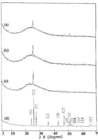
FIG. L XRD patterns of the as-deposited films prepared by PLE tech-nique at different substrate temperatures: (a) room temperature (30 'C), (b) l50'C, and (cl 250'C; (d) is the pattern of CdS powders.
films were smooth and the films adhered firmly to the sub-strate. The color of a film surface was transparently yel-lowish.
The structures of the as-deposited films were analyzed by x-ray diffraction (XRD) with Cu Ka source (A
=
1.54 A). Figure 1 shows the XRD results of the films deposited by PLE technique at substrate temperature of (a) 30°C, (b) 150 ·C, and (c) 250 ·C, and (d) is the XRD spectrum for the CdS powder. The thickness of these films are ~ 900 A, The pattern of powder agrees well with the previous result for the wurzite structure of CdS. The higher back-ground intensity in the Bragg angle of 20· to 3D· is due to the Corning glass. All the films have high orientation in (002) direction which increases as the substrate tempera-ture increases. K wok et al.14 reported that high oriented film in (002) and (004) was obtained by using Ar F exci-mer laser (193 nm and 10 pps) at substrate temperature higher than 350 ·C. Comparing our result with theirs, one can see we obtained a preferred orientation at lower growth temperatures. This improvement is mainly due to our deposition rate (-0.07 A/pulse, repetition rate 1 pps) is much lower than that of Kwok et al (~0.3 A/pulse, repetition rate 10 pps), The deposition of high orientation films at the low temperature substrate (room temperature to 250°C) which is able to avoid interditfusion should be regarded as a significant improvement in the PLE tech-nique. Figure 2 shows the XRD spectrum of as-deposited films by TE technique. Spectrum (a) represents the struc~486 Dai et sl.: High orientation CdS thin films
n
65 60 50 40 30 20 2
e
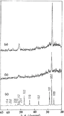
(degree)FIG. 2. XRD patterns of the as-deposited films prepared by TE technique
at different substrate temperatures: (a) without preheating and (b) 200 'C; (c) is the pattern of CdS powders. In case (a) the substrate temperature is measured before the deposition.
ture of film with thickness 3700
A
and substrate at room temperature, while spectrum (b), the thickness is 3200A
and substrate at 200 ·C. From these XRD pattern, they reveal that these films have high preference direction in (002) no matter what the substrate temperature is. Like-wise, these results are better than the previous works 7,9with the same TE technique. The reason for this improve-ment in our TE technique might be due to radiant heating (the surface of the substrate is estimated at -100 ·C) from the high temperature of the tungsten basket (-1030 ·C). However, when we compared our TE films with our PLE films which were deposited at nearly the same substrate temperature (150 ·C) and with same thickness (== 900 A), we found that the XRD spectra for both films are nearly the same except the linewidth of the XRD peak for the PLE films is sharper than that of the TE films. This dis-crepancy will be explained in detail in the following para-graphs.
The surface morphology of the as-deposited films were studied by scanning electron microscope. The surface of PLE samples were very smooth optically. No visible struc-ture could be observed under X 8000 multiplying. How-ever, there were a few whitish spots on the surface of TE samples. These particulates or precipitates are due to the rapidly heating effect of TE process (heating the basket to 1030 ·C within less than 1 min).
J. Vac. Sci. Technol. A, Vol. 10, No.3, May/Jun 1992
lLO
2LO
200 400 600 800 1000 1200 1400 Raman shift (em-i)
486
FIG. 3. The Raman spectra of the as-deposited films: spectrum (a) is the
result of PLE technique at substrate temperature of 250 ·C; spectrum (b) is the result of TE technique at substrate temperature of 200 ·Co
It is well known that Raman scattering spectra can give useful information about the crystalline of the film by eval-uating the spectral peak position and the spectral width of the Raman spectra. However, few work2o about the Raman study of CdS film is devoted. The 4880
A
line of an Ar +laser was used as an excitation source for the Raman ex-periment. Spectra were taken at room temperature in the 45° reflection geometry with the samples placed under the micrometer stage of a triple grating spectrograph (Spex 1877C) equipped with liquid nitrogen cooled CCD detec-tors array (Photometries CC200). The incident power on the sample was about 100 mW. The slit widths used led to a resolution of 3 em - I. The spectrum is corrected by neon
lamp. A typical Raman spectra of the as-deposited CdS thin films grown by PLE (spectrum a, substrate at 250 ·C) and TE (spectrum b, substrate at 200 ·C) techniques are shown in Fig. 3. The spectra show that there are four Raman peaks, which can be identified by comparing the spectra obtained by previous works (such as in the inves-tigation for bulk CdS crystals21 and for CdS crystallites in aqueous solution22 and in glass waveguides23), in PLE
films. However, three peaks are observed in TE films. It
should be noted that this is the first time for as many as four overtones to be observed by 4880
A
excitation on PLE films. The first peak is a lLO (longitudinal optical) pho-non peak and the others are 2LO, 3LO, and 4LO over-tones. The LO phonon frequency for a single crystal of CdS was given in the literature21 as 305 cm - 1, while thevalues measured by us were as low as 300 cm - I and 297
em - 1 in PLE and TE films, respectively. This lower
fre-quency shift is attributed to the effect caused by the grain size,20,21-23 i.e., the effect of dimensions on the vibrational properties in small crystalline. The manifested
discrepan-487 Cal et si.: High orientation CdS thin films
TABLE 1. Grain size (in angstroms) of the (002) plane deposited by PLE
and TE techniques at different substrate temperatures, Substrate temperature eC)
Techniques 30 150 200 250
PLE 291 A 408 A 510 A
TE 204 A 255 A
des on the shape and shift of Raman peaks between two deposition techniques are due to the structure and grain size of the films. As is well known, the crystallite size can be estimated by the formula d
=
Q,9AID cos it, where A is the x-ray wavelength, D is the angular line width at half-maximum intensity (in radian), and {} is the Bragg angle, The values of the grain size d were calculated as listed in Table I. For both deposition techniques, the grain sizes increase as the substrate temperature getting higher. This is because of the mobility of evaporants on the substrate in-creases when the substrate temperature inin-creases. Mean-while, the grain sizes of CdS films deposited by using PLE technique are larger than those grown by TE technique. This is due to the species from PLE evaporation have higher kinetic energy (-10 eV range) 16 than the thermalevaporation (~O.l eV range). The films deposited by PLE method obviously have larger crystallites size which is the major cause to have sharper peaks and smaller shifts in Raman spectra,
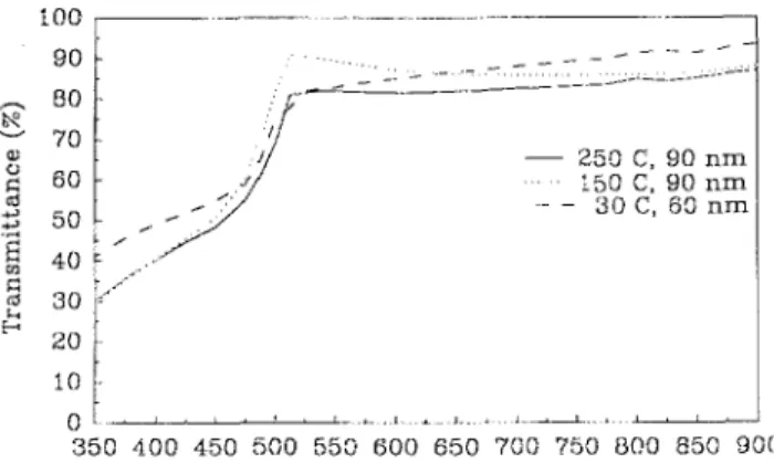
The transmittance T of the as-deposited films were mea-sured at normal light incidence in the wavelength range 350-900 nm using a double-beam spectrophotometer (Shi-madzu UV-21OA). Figs. 4 and 5 show representative ex-amples of the spectral dependence of the transmittance for several substrate-temperature dependence of CdS films by PLE and TE techniques, respectively. The absorption at ~ 510 nm agreed well with that of bulk materiaL The transmittance curves below absorption edge are highly thickness dependence which have the same tendency as the work by EI-Nahass et al.24 The substrate temperature is an insensitive parameter for both the methods as shown in
100 c -90 - --
---.~
. 'I
~l.·
",/1"
.~
40~//
~~~=-- ~-----
--- 250 C 90 nm 150 C: 90 nm .- - 30 C, 60 nm ~ 30 ~~/ H E-< 20 10 o ! ~L "1- .. ,,,-" L _ . " L_~" L . ~, ~-L-~ 350 400 450 500 550 600 650 700 750 800 850 900 Wavelength (nm)FIG. 4. The spectral dependence of the transmittance for the as-deposited films prepared by PLE technique at different substrate temperatures.
J. Vac. Sci. Technol. A, Vol. 10, No.3, May/Jun 1992
487
g
OJ C) .:: <J ... ...,'s
OJ ~ oj ... E-< Wavelength (nrn)FIG, 5, The spectral dependence of the transmittance for the as-deposited
films prepared by TE technique at substrate temperatures of 200·C (open
circles), 150'C (6,), lOO'C (A) and without preheating (e).
figures. The transmittances above the absorption edge from both methods are all in the range of 85%-95% which is much higher than that obtained by Kwok et al.14
High transparency properties of these films are able to be used as the window of solar cells_ Finally, we must point out that the absorption edge of the thinner films by TE tech-nique in Fig. 5 are shifted to lower wavelength. It can be a manifestation of a small degree quantum size effect due to confinement of electron or hole in small volume microcrystallites.25
IV. CONCLUSION
In conclusion, we have grown the undoped CdS films by PLE and TE techniques on Corning's 7059 glass at differ-ent substrate temperatures. The structure and optical transmittance of the as-deposited films are compared, The results show that films with highly orientation in (002) and transparency in the range of 85%-95% have been obtained by both methods. On the other hand, the PLE films have sharper peaks, more overtones and smaller Ra-man shift in the RaRa-man studies. These properties are con-tributed by larger grain size. Therefore, PLE method is suitable for the applications of depositing CdS thin film in which the substrate can be affected by high temperature process.
ACKNOWLEDGMENT
This work has been partially financed by the National Science Council, Taiwan (ROC), under the Grant No . NSC 80-0208-M-009-2S.
I ], A, Bragagnolo, A. M. Barnett, J, E. Phillips, R. H. Hall, A.
Roth-warf. and J. D. Meakin, IEEE Trans. Electron, Devices 27. 645
( 1980),
2S. Wagner, J. L. Shay, K. 1. Bachman, and E. Buehler, Appl. Phys.
Lett. 26, 229 (1975).
JR, R. Arya, P. M. Sarro, and J. J. Loferski, AppL Phys. Lett. 41, 355
(1982),
4c.
Cali, V. Daneu, A. Orioli, and S. Riva-Sansevirino, AppL Opt. 15,488 Oal et sl.: High orientation CdS thin films
5y. Daneu, D. P. DeGloria, A. Sanchez, F. Tong, and R, M. Osgood,
Jr., Appl. Phys. Lett. 49, 546 (1986).
oM. Dagenais and W. F. Shamn, Appl. Phys. Lett. 46, 230 (1985).
7N. Romeo, G. Sberveglieri, and L. Tarricone, Thin Solid Films, 43,
LIS (1977).
sR. R. Arya, R. Beaulieu, M. Kwietniak, and J. Loferski, J. Yac. Sci. Techno!. 20, 306 (1982).
9T. Hayashi, T. Nishikura, T. Suzuki, and Y. Ema, J. Appl. Phys. 64, 3542 (l988).
11'. H. Weng, J. Electrochem. Soc. 126, 1820 (1979).
lly. Canevari, N. Romeo, G. Sberveglieri, S. Azzi, A. Tosi, M. Curti,
and L. Zanotti, J. Yac. Sci. Techno!. A 2, 9 (1984).
12H. Uda, S. Ikegami, and H. Sonomura, Jpn. J. Appl. Phys. 29, 30 (1990).
131. Marti!, G. Gouzalez-Diaz, and F. Sanchez-Quesada, J. Yac. Sci. Techno!. A 2, 1491 (1984).
14H. S. Kwok, J. P. Zheng, S. Witanachchi, P. Mattocks, L. Shi, Q. Y.
Ying, X. W. Wang, and D. T. Shaw, App!. Phys. Lett. 52,1095 (1988).
J. Vac. Sci. Technol. A, Vol. 10, No.3, May/Jun 1992
488
ISB. Stjerna and C. G. Granguist, App!. Opt. 29, 447 (1990). 16J. T. Cheung, and H. Sankur, CRC Crit. Rev. Solid State Mater. Sei.
15, 63 (1988).
17C. M. Dai, C. S. Su, and D. S. Chuu, Appl. Phys. Lett. 57, 1879 (1990).
ISC. M. Dai, C. S. Su, and D. S. Chuu, J. App!. Phys. 69, 3766 (1991). 19C. M. Dai, K. S. Wu, W. F. Hsieh, and D. S. Chuu, Rev. Sci. Instrum.
61, 3713 (1990).
20J. F. Scott and T. C. Darnen, Opt. Commun. 5, 410 (1972). 21R, J. Briggs, and A. K. Ramdas, Phys. Rev. B 13, 5518 (1976).
22R, Rossetti, S. Nakahara, and L. E. Brus, J. Chern. Phys. 82, 552
(1985)
23H. Jerominek, M. Pigeon, S. Patela, Z. Jakubczk, C. Delisle, and R. Tremblay, J. Appl. Phys. 63, 957 (1988).
24M. M. EI-Nahass, O. Jamjoum, S. M. AI-Howaity, and K. Abdel-Hady, J. Mater. Sci. Lett. 9, 79 (1990).
251. Tanahashi, A. Tsujimura, T. Mitsuyu, and A. Nishino, Jpn. J. App!. Phys. 29, 2111 (1990).