www.MaterialsViews.com
COMMUNICATION
Ming-Shin Su , Chih-Yin Kuo , Mao-Chuan Yuan , U-Ser Jeng , Chun-Jen Su ,
and Kung-Hwa Wei *
Improving Device Effi ciency of Polymer/Fullerene
Bulk Heterojunction Solar Cells Through Enhanced
Crystallinity and Reduced Grain Boundaries Induced
by Solvent Additives
M.-S. Su , C.-Y. Kuo , M.-C. Yuan , Prof. K.-H. Wei Department of Materials Science and Engineering National Chiao Tung University
1001 Ta Hsueh Road, Hsinchu 30050, Taiwan, ROC E-mail: [email protected]
Dr. U.-S. Jeng , Dr. C.-J. Su
National Synchrotron Radiation Research Center 101 Hsin-Ann Road, Science-Based Industrial Park Hsinchu 30077, Taiwan, ROC
DOI: 10.1002/adma.201101274
Polymer solar cells based on bulk heterojunction (BHJ) struc-tures, featuring conjugated polymers as donors and fullerene derivatives as acceptors, [ 1 ] are being developed for their poten-tial application in the low-cost fabrication of large-area devices. In recent reports, BHJ solar cells incorporating crystalline or low-bandgap conjugated polymers [ 2 ] and fullerene derivatives have exhibited maximum power conversion effi ciencies (PCEs) of up to 8%. [ 3 ] The morphology [ 4 ] of the active layer in a BHJ solar cell incorporating a polymer/fullerene thin fi lm plays a critical role affecting the device performance; phase-separated domains in the active layer provide not only interfaces for charge separation of photogenerated excitons but also perco-lation pathways for charge carrier transport to the respective electrodes, critically affecting the device’s PCE. The nanoscale morphology of a polymer/fullerene thin fi lm is greatly affected by (i) the fi lm processing conditions, [ 5 ] (ii) the molar ratio (composition) of the polymer and the fullerene, [ 6 ] and (iii) the nature of the solvent additive (if any). [ 7 ] In particular, BHJ polymer solar cells can exhibit improved device performance after undergoing thermal or solvent annealing or the incorpora-tion of solvent additives, all of which alter the fi lm morphology to a more favorable state relative to that of the as-cast fi lm or the fi lm in the absence of the additive, presumably resulting from (i) self-organization of the polymer units into ordered structures and (ii) appropriate aggregation of fullerene domains to provide percolation networks for charge carrier transport. [ 6 , 8 ] Among these approaches, the addition of solvent additive during the processing of the active layer is the simplest and most effective means of optimizing a BHJ device’s morphology; it infl uences the size of the fullerene domains and enhances the crystallinity of the self-organized polymers by improving the solubility of
the fullerenes and slightly elongating the drying time of the active layer. Although chloroform and chlorobenzene provide good solubility for conjugated polymers, they are relatively poor solvents for asymmetric C 70 -fullerene derivatives such as PC 71 BM; therefore, the need exists for a solvent additive that can bridge the miscibility gap between the conjugated polymer and PC 71 BM so that more-homogeneous fi lms can be produced. Notably, 1,8-di( R )octanes, with different functional groups R , can signifi cantly improve the miscibility of PC 71 BM with the polymer. [ 7 ] Moreover, the alkyl chain length of the additive can have a substantial effect on the morphology of the active layer and, therefore, the device’s performance. [ 9 ] The precise effects of solvent additives on the morphologies of active layers consti-tuted by crystalline polymers and fullerenes are not fully under-stood because of insuffi cient structural information extending from the nano- and meso-range.
In this Communication, we demonstrate that the PCE of a device incorporating a PBTTPD/PC 71 BM (1:1.5, w/w) fi lm as the active layer can be improved from 5% to 7.3% – a rela-tive increase of 45% – after incorporating 1,6-diiodohexane (DIH), an additive of suitable alkyl chain length, during solu-tion processing. We also elucidated the precise active layer morphology with simultaneous synchrotron grazing-incidence small-/wide-angle X-ray scattering (GIWAXS/GIWAXS) and transmission electron microscopy (TEM) and found that the additive DIH not only induced higher polymer crystallinity (2.4 and 3.6 times in the out-of-plane and in-plane direc-tions, respectively), but also decreased the average size of the aggregated fractal-like PC71BM clusters to 30 nm (from 150 nm for the fi lm without additives) by removing their grain boundaries.
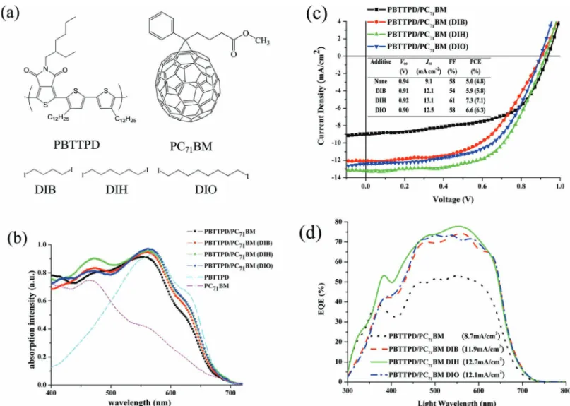
Figure 1 a presents the molecular structures of poly-{bi(dodecyl)thiophene-thieno[3,4- c ]pyrrole-4,6-dione} (PBTTPD), [ 10 ] {6}-1-(3-(methoxycarbonyl)propyl)-{5}-1-phenyl-[5,6]-C 71 (PC 71 BM), and the solvent additives DIH, 1,4-diiodo-butane (DIB), and 1,8-diiodooctane (DIO), which, along with chloroform (CF), we used to process the active layer. Figure 1 b displays the UV–vis absorption spectra of PBTTPD/PC 71 BM (1:1.5, w/w) fi lms cast with 0.5 vol% of DIB, DIH, and DIO in CF. The intensity of the signal between 400 and 500 nm for the PBTTPD/PC 71 BM fi lm increased substantially and the peak maximum blue-shifted relative to that of the pristine PBTTPD fi lm because of the additional absorption in this region provided
www.MaterialsViews.com
COMMUNICATION
the three solvent additives were all greater than 12 mA cm − 2 , signifi cantly increased from the value of 9 mA cm − 2 for the PBTTPD/PC 71 BM active layer that had been processed without any solvent additive. Specifi cally, the photovoltaic device based on PBTTPD/PC 71 BM processed with DIH as the solvent addi-tive exhibited the highest short-circuit current density; it was 40% greater than that obtained without solvent additives. More-over, the FF for the device containing the PBTTPD/PC 71 BM active layer that had been processed with DIH was the highest among all of these studied devices. As a result, the PCE of the device incorporating the PBTTPD/PC 71 BM active layer that has been processed with DIH as the solvent additive increased to 7.3% from 5.0% for the corresponding device prepared without any solvent additive. Thus, an optimum chain length exists for the solvent additives’ molecular structure to improve the mor-phology of the active layer and, therefore, device performance.
Figure 1 d displays the external quantum effi ciencies (EQEs) of the devices containing PBTTPD/PC 71 BM active layers that had been processed with solvent additives. The PBTTPD/PC 71 BM devices processed with solvent additives displayed signifi cantly by PC 71 BM and because the existence of PC 71 BM disrupted the
packing and ordering of PBTTPD. When we incorporated DIB, DIH or DIO as an additive for processing, the UV–vis absorp-tion peak of the resultant PBTTPD/PC 71 BM fi lms red-shifted slightly, relative to that of the PBTTPD/PC 71 BM fi lm prepared in the absence of any additives, but retained its vibronic peak at 630 nm. The PBTTPD/PC 71 BM fi lm processed using DIH dis-played slightly higher absorption between 400 and 500 nm than did the PBTTPD/PC 71 BM fi lms processed with DIB or DIO, presumably because of differences in the degrees of dispersion of PC 71 BM in PBTTPD.
Figure 1 c displays the photovoltaic performances of the devices incorporating PBTTPD/PC 71 BM fi lms that had been processed with the different solvent additives; the inset lists their open-circuit voltages ( V oc), short-current densities ( J sc ), and fi ll factors (FF). The open-circuit voltages of the devices featuring PBTTPD/PC 71 BM active layers were all approximately 0.9 V, regardless of whether they were processed with or without solvent additives. The short-current densities of the devices with PBTTPD/PC 71 BM active layers that had been processed with
Figure 1 . (a) Molecular structures of PBTTPD, PC 71 BM, and the solvent additives DIB, DIH, and DIO. (b) Absorption spectra of PBTTPD/PC 71 BM fi lms
processed from CF (square) and from CF containing 0.5 vol% DIB (circle), DIH (triangle), and DIO (inverted triangle). (c) Current density–voltage curves of PBTTPD/PC 71 BM devices processed from CF (square) and from CF containing 0.5 vol% DIB (circle), DIH (triangle), and DIO (inverted
tri-angle). The obtained values of V oc and J sc and the FFs and PCEs are listed in the inset table; averaged PCEs are presented in brackets. (d) EQE curves
of PBTTPD/PC 71 BM devices processed from CF (black dashed line) and from CF containing 0.5 vol% DIB (red dotted line), DIH (green line), and DIO
www.MaterialsViews.com
COMMUNICATION
different phases present in the same spot. Figure 2 b presents GISAXS profi les recorded along the in-plane direction, q x , of the 2D images for ca. 90-nm-thick PBTTPD/PC 71 BM (1:1.5, w/w) fi lms that had the same composition as those used in the active layers of the devices. The scattering intensity in the in-plane direction, I ( q x ), for the PBTTPD/PC 71 BM fi lms processed with or without additives exhibited the same power-law scattering behavior with respect to the in-plane wavevector q x [i.e., I ( q x )
μ q x − D ], with the fractal dimension D of approximately 3 (in the region of q x greater than ca. 0.01 Å − 1 ) indicating a fractal-like (porous) PC 71 BM aggregate. Notably, the values of I ( q x ) similarly measured for the P3HT/PC 61 BM (1:1, w/w) fi lm after thermal annealing (150 ° C, 15 min) revealed characteristically different scattering behavior in the q x region > 0.01 Å − 1 , due to denser packing of the PC 61BM aggregates. Additionally, the inset in the lower-left-hand corner of Figure 2 (b) displays a corresponding 2D GISAXS pattern, with strong interference peaks at a value of q x of 0.00183 Å − 1 , revealing a large mean enhanced EQEs relative to that for the device with the active
layer processed without any solvent additive. The measured short-circuit currents for the devices incorporating PBTTPD/ PC 71 BM active layers processed using DIB, DIH, and DIO were 12.1, 13.1, and 12.5 mA cm − 2 , respectively; the short-circuit cur-rents obtained from integrating the EQE curves were 11.9, 12.7, and 12.1 mA cm − 2 , respectively [inset to Figure 1d]; these values are within a 5% error range, indicating the accuracy of our measurements. The fact that the device incorporating the DIH-processed active layer exhibited the highest EQE is consistent with the strong absorption intensity it displays in Figure 1 b, implying that it might possess a more favorable active layer morphology.
Figure 2 a displays the coordinated GIWAXS and GISAXS set-up that we used to simultaneously deduce the orienta-tion and crystallinity of the PBTTPD crystal lamellae and the aggregation of PC 71 BM on length scales of up to a few tens of nanometers, respectively, in the thin fi lms; this setup can behave as a precise and statistically meaningful probe of the
Figure 2 . (a) Schematic representation of the GIWAXS and GISAXS set-up; q z and q x denote X-ray scattering in the out-of-plane and in-plane
direc-tions, respectively. (b) In-plane GISAXS profi les of the PBTTPD/PC 71 BM fi lms spin-cast in the absence (square) and presence of DIB, DIH or DIO, as
indicated. Insets showed GIWAXS patterns of the fi lms processed in the absence and presence of DIH. The data were fi tted (dashed or solid curves) using a model of fractal aggregates, as described in the text. The GISAXS spectrum of the P3HT/PCBM fi lm was fi tted (dashed curve) using polydisperse spheres. (c) TEM images of PBTTPD/PC 71 BM fi lms prepared (left) in the absence and (right) presence of the additive DIH. (d) Out-of-plane GIWAXS
www.MaterialsViews.com
COMMUNICATION
with and without the additive DIH; the bright and dark regions correspond to PBTTPD- and PCBM-rich domains, respectively, because the differences in the electron scattering densities of fullerenes (1.5 g cm − 3 ) and polymers (1.1 g cm − 3 ) are quite large. Large PC 71 BM grains (size: ca. 150 nm; mean spacing: ca. 340 nm) are evident in the image of the fi lm processed without any additive while the size of PC 71 BM grains reduced to ca. 30 nm for the PBTTPD/PC 71 BM fi lm prepared with DIH as the additive. These morphological differences induced by the additives in the mesoscale are consistent with our GISAXS results; the internal structures of the 150-nm grains (consisting spacing of 343 nm formed by a monolayer of aggregated
clus-ters in the in-plane direction of the fi lm. In contrast, the inset in the upper-right-hand corner of Figure 2 (b) reveals no such interference peaks for the PBTTPD/PC 71 BM fi lm prepared with DIH as the additive. Moreover, the power law scattering behavior for the scattering intensity in the in-plane direction of the PBTTPD/PC 71 BM fi lms processed with the additives fades out in this low- q x region ( < 0.007 Å − 1 ), implying a cluster size of a few tens of nanometers. To characterize the PC 71 BM fractal clustering size, 2 ξ , we fi tted the I ( q x ) data from the PBTTPD/ PC 71 BM fi lms processed with or without additives using a fractal model (see the Supporting Information) and a universal fractal dimension D of approximately 3. The fi tted PC 71 BM fractal cluster sizes (2 ξ ) for the PBTTPD/PC 71 BM fi lms proc-essed without any additive and with DIB, DIH, and DIO were 40, 36, 32, and 39 nm, respectively.
From the GISAXS analysis, we conclude that the active layers processed with the additives featured smaller and better-dispersed PC 71 BM domains and, therefore, formed better net-work morphologies than that the fi lm cast without any solvent additives. Among the tested additives, DIH provided the fi nest dispersion of PC 71 BM, presumably because it optimized the balance between the solubility of PC 71 BM and the interactions between the additive and the polymer molecules. Figure 2 (c) dis-plays TEM images of PBTTPD/PC 71 BM (1:1.5, w/w) fi lms cast
Table 1. Structure parameters for PBTTPD/PC 71 BM fi lms processed with
and without additives; 2 ξ is the size of the fractal clusters of PC 71 BM; χ
and L are the relative crystallinity and edge-on (or face-on) lamellar size, respectively, of the conjugate polymer.
Additive 2 ξ (nm) (PC 71 BM) χ (%) (edge-on lamellae) (100) out-of-plane L (nm) (edge-on lamellae) (100) out-of-plane χ (%) (face-on lamellae) (100) in-plane L (nm) (face-on lamellae) (100) in-plane None 40 ± 2 21 31 3 3 DIB 36 ± 1 26 24 9 11 DIH 32 ± 1 49 24 11 13 DIO 39 ± 1 41 24 10 13
Figure 3 . Schematic representations of mesograins in PBTTPD/PC 71 BM fi lms processed in the (left) absence and (right) presence of an additive.
In the presence of the additive, the mesoscale grains dissolved into smaller fractal clusters; the additive also intercalated with the PBTTPD lamellar nanodomains. The fractal-like P 71 CBM clusters were circular objects fi lled with interconnected PC 71 BM units.
www.MaterialsViews.com
COMMUNICATION
Acknowledgements
We thank the National Science Council for fi nancial support (NSC 99–2120-M009–003).
Received: April 5, 2011 Revised: May 6, 2011 Published online: June 14, 2011
of 40-nm clusters), respectively in the PBTTPD/PC 71 BM fi lms processed without any additive.
Figure 2 d presents the detailed out-of-plane and in-plane direction intensities of the PBTTPD/PC 71 BM (1:1.5, w/w) fi lms processed with and without additives. The strong out-of-plane (100) peak at a value of q z of 0.24 Å − 1 is due to edge-on PBTTPD lamellae; the amorphous halo centered at a value of q z of 1.26 Å − 1 corresponds to short-range ordering caused by the PC 71 BM aggregates in the PBTTPD/PC 71 BM fi lms. One additional char-acteristic peak was present for the PBTTPD/PC 71 BM fi lms that had been processed with DIB, DIH, and DIO as additive: an out-of-plane (010) signal at a value of q z of 1.7 Å − 1 . This weak signal resulted from face-on PBTTPD lamellae or from π – π stacking of the PBTTPD units; these face-on lamellae would also result in an in-plane (100) peak at a value of q x of ca. 0.24 Å − 1 . The inset to Figure 2 d reveals that the intensities of the in-plane (100) peaks at a value of q x of ca. 0.24 Å − 1 for the PBTTPD/PC 71 BM fi lms proc-essed with the additives were enhanced relative to that of the fi lm processed without any additives, with the largest increase in the case of DIH as the additive. Table 1 summarizes the corresponding lamellar spacings and sizes estimated from the Scherrer equation and the relative crystallinities from the integrated intensities of the (100) peaks for the edge-on and face-on PBTTPD lamellae. The introduction of the additives during processing enhanced the crystallinity of both the edge-on and face-on PBTTPD lamellae, with slightly reduced edge-on lamellar sizes and increased face-on lamellar sizes. The PBTTPD/PC 71 BM fi lm processed with DIH as the additive displayed higher crystallinity—2.4 times and 3.6 times for the PBTTPD edge-on lamellae and face-on lamellae, respectively—as large as that of the PBTTPD/PC 71 BM fi lm that had been cast without any additive. Therefore, DIH provided superior results, compared with DIB and DIO, when used as the additive for the PBTTPD/PC 71 BM fi lm. Nevertheless, the opti-mized chain length of this diiodoalkane might not necessarily be appropriate for other homologous systems; the polarity of the additive, with respect to the specifi c conjugate copolymer and PC 71 BM, must be taken into consideration.
Figure 3 presents schematic representations of the PBTTPD/ PC 71 BM morphologies that are consistent with the structural information obtained from the GISAXS, GIWAXS, and TEM analyses. These drawings depict the additive not only inducing higher polymer crystallinity in both the out-of-plane and in-plane directions but also removing the grain boundary of the aggregated fractal-like PC 71BM clusters, leading to superior pathways for carrier transport.
In conclusion, we have fabricated a BHJ solar cell device incorporating a PBTTPD/PC 71BM thin fi lm that exhibited a PCE of 7.3% when the active layer was processed with DIH, a diiodoalkane additive, which effectively induced higher polymer crystallinity and removed the grain boundary of the large PC 71 BM-rich grains, resulting in a more-uniform fi lm morphology on the mesoscale.
Supporting Information
Supporting Information is available from the Wiley Online Library or from the author.
[ 1 ] G. Yu , J. Gao , J. C. Hummelen , F. Wudl , A. J. Heeger , Science 1995 , 270 , 1789 .
[ 2 ] a) H. Y. Chen , J. Hou , S. Zhang , Y. Liang , G. Yang , Y. Yang , L. Yu , Y. Wu , G. Li , Nat. Photon. 2009 , 3 , 649 ; b) Y. Liang , Y. Wu , D. Feng , S. T. Tsai , H. J. Son , G. Li , L. Yu , J. Am. Chem. Soc. 2009 , 131 , 56 ; c) S. H. Park , A. Roy , S. Beaupre , S. Cho , N. Coates , J. S. Moon , D. Moses , M. Leclerc , K. Lee , A. J. Heeger , Nat. Photon. 2009 , 3 , 297 ; d) F. Huang , K. S. Chen , H. L. Yip , S. K. Hau , O. Acton , Y. Zhang , J. Luo , A. K. Y. Jen , J. Am. Chem. Soc. 2009 , 131 , 13886 ; e) C. V. Hoven , X. D. Dang , R. C. Coffi n , J. Peet , T. Q. Nguyen , G. C. Bazan , Adv. Mater. 2010 , 22 , E63 ; f) C. Piliego , T. W. Holcombe , J. D. Douglas , C. H. Woo , P. M. Beaujuge , J. M. J. Fréchet , J. Am.
Chem. Soc. 2010 , 132 , 7595 ; g) Y. Zhang , S. K. Hau , H. L. Yip ,
Y. Sun , O. Acton , A. K.-Y. Jen , Chem. Mater. 2010 , 22 , 2696 ; h) T. Y. Chu , J. Lu , S. Beaupré , Y. Zhang , J. R. Pouliot , S. Wakim , J. Zhou , M. Leclerc , Z. Li , J. Ding , Y. Tao , J. Am. Chem. Soc. 2011 , 133 , 4250 ; i) G. Y. Chen , Y. H. Cheng , Y. J. Chou , M. S. Su , C. M. Chen , K. H. Wei , Chem. Comm. DOI: 10.1039/c1cc10585j.
[ 3 ] M. A. Green , K. Emery , Y. Hishikawa , W. Warta , Prog. Photovolt: Res.
Appl. 2011 , 19 , 84 .
[ 4 ] a) H. Sirringhaus , P. J. Brown , R. H. Friend , M. M. Nielsen , K. Bechgaard , B. M. W. Langeveld-Voss , A. J. H. Spiering , R. A. J. Janssen , E. W. Meijer , P. Herwig , D. M. de Leeuw , Nature 1999 , 401 , 685 ; b) M. C. Quiles , T. Ferenczi , T. Agostinelli , P. G. Etchegoin , Y. Kim , T. D. Anthopoulos , P. N. Stavrinou , D. D. C. Bradley , J. Nelson , Nat.
Mater. 2008 , 7 , 158 ; c) H. Ma , H. L. Yip , F. Huang , A. K.-Y. Jen , Adv. Funct. Mater. 2010 , 20 , 1371 .
[ 5 ] a) G. Li , Y. Yao , H. Yang , V. Shrotriya , G. Yang , Y. Yang , Adv. Funct.
Mater. 2007 , 17 , 1636 ; b) F. Padinger , R. S. Rittberger , N. S. Sariciftci ,
Adv. Funct. Mater. 2003 , 13 , 85 ; c) R. Hamilton , C. G. Shuttle , B. O’Regan , T. C. Hammant , J. Nelson , J. R. Durrant , J. Phys. Chem.
Lett. 2010 , 1 , 1432 ; d) L. M. Chen , Z. Xu , Z. Hong , Y. Yang , J. Mater. Chem. 2010 , 20 , 2575 .
[ 6 ] a) M. Y. Chiu , U. Jeng , M. S. Su , K. H. Wei , Macromolecules 2010 , 43 , 428 ; b) S. S. van Bavel , M. Barenklau , G. de With , H. Hoppe , J. Loos , Adv. Funct. Mater. 2010 , 20 , 1458 ; c) A. C. Mayer , M. F. Tony , S. R. Scully , J. Rivnay , C. J. Brabec , M. Scharber , M. Koppe , M. Heeney , I. McCulloch , M. D. McGehee , Adv. Funct.
Mater. 2009 , 19 , 1173 .
[ 7 ] a) J. K. Lee , W. L. Ma , C. J. Brabec , J. Yuen , J. S. Moon , J. Y. Kim , K. Lee , G. C. Bazan , A. J. Heeger , J. Am. Chem. Soc . 2008 , 130 , 3619 ; b) J. M. Szarko , J. Guo , Y. Liang , B. Lee , B. S. Rolczynski , J. Strzalka , T. Xu , S. Loser , T. J. Marks , L. Yu , L. X. Chen , Adv. Mater. 2010 , 22 , 5468 ; c) J. T. Rogers , K. Schmidt , M. F. Toney , E. J. Kramer , G. C. Bazan , Adv. Mater. DOI: 10.1002/adma.201003690; d) M. S. Su , H. C. Su , C. Y. Kuo , Y. R. Zhou , K. H. Wei , J. Mater. Chem. 2011 , 21 , 6217 .
[ 8 ] M. Y. Chiu , U. Jeng , C. H. Su , K. S. Liang , K. H. Wei , Adv. Mater. 2008 , 20 , 2573 .
[ 9 ] J. Peet , J. Y. Kim , N. E. Coates , W. L. Ma , D. Moses , A. J. Heeger , G. C. Bazan , Nat. Mater. 2007 , 6 , 497 .
[ 10 ] M. C. Yuan , M. Y. Chiu , S. P. Liu , C. M. Chen , K. H. Wei ,