Electrical and Optical Reliability Improvement of HfOz Gate
Dielectric by Deuterium and Hydrogen Incorporation
C.
-Y.
Yu',T. C.
Chena,M. H.
Lee', S.-H. Huang", L.S.
Leeb, a n d C.W.
Liu"bb.* aDepartment o f Electrical Engineering and GraduateInstitute of Electronics Engineering,
National
Taiwan
University,Taipei, Taiwan
'Electronics Research & Service Organization, Industrial Technology Research Institute
(ERSOIITRI), Hsinchu, T a i w a n
Phone: 886-2-2363525 1 ext.5 15 Fax: 886-2-23638247 *Email: [email protected]
Absirael
Electrical and optical reliability characteristic of Pt/Ht02 gate stack have been investigated. Incorporating deuterium and hydrogen treatment during post-metallization annealing is employed to improve both the electrical and optical reliability of Pt/HfOz gate stack. For comparison, deuterium-treated technology provides slightly better reliability improvement on both the electrical and optical reliability of Pt/HfOZ gate stack devices.
1. Introduction
High dielectric constant (high-k) materials implemented in CMOS technologies as gate dielectrics will eventually be needed to relieve the rapid gate current increase associated with aggressive oxide thickness scaling. The increased dielectric constant allow for increased physical thickness at similar driving capability. Among the many potential high-k materials under investigation, Hf0, films have been widely considered one of the most promising candidates because of its relative high electric constant ( E
-
20) and low leakage current density (103-106less than SiOl of equivalent CET). Optimization of interfacial layer and hulk high-k layer is known to be important due to the instability is one of the most challenging issues to implement high-k gate dielectric. Several studies on HfOz have been reported with the polysilicon gates electrode [I, 21.
Metal gate electrodes are generally well accepted to eliminate gate depletion effect, additional polysilicon gatedhigh k interfacial layer, and high gate resistance problems that are associated with conventional polysilicon gates. In addition to gate depletion, recently polysilicon gates have also shown to suffer from Fermi level pinning on high-k dielectrics [ 3 ] . These issues warrant the investigation
ofmetallic gate electrodes on high-k dielectrics. In this paper, we will present both the electrical and optical reliability improvement of PtiHfO, gate stack by deuterium and hydrogen incorporation.
2. Experiment
The HfO, films were deposited by atomic layer chemical vapor deposition (ALCVD) [4] on the p-type, 1-10 n c m , (001) orientation silicon substrate wafers, followed by a post-deposition-annealing (FDA) at 600
"C
for 300 sec in NZ by rapid thermal annealing (RTA). ALD might be theleading deposition process for High-K gate dielectrics [5,6] due to its thickness control and good conformality. In ALD, materials are deposited layer by layer in a self-limiting fashion, allowing for inherent atomic scale control. The metal-insulator-silicon (MIS) capacitor structure had Pt gate electrode with circular areas defined by the shadow mask. Pt electrodes were deposited using DC magnetron sputtering. The area of capacitor was 3 x 10~4 cm2. The A I contact is on the back of the wafers. The furnace post-metallization annealing was done in forming gas to incorporate deuterium
(D2 / NZ=l / 9) and hydrogen (H2 / NZ=l / 9) at 400
"C
for 30 min. In this experiment, the C-V, I-V characteristics, and reliability measurement was carried out using an HP 41 56A semiconductor parameter analyzer. Time evolutions of light emission intensity measurement are employed to examine the optical reliability.3. Results and Discussion
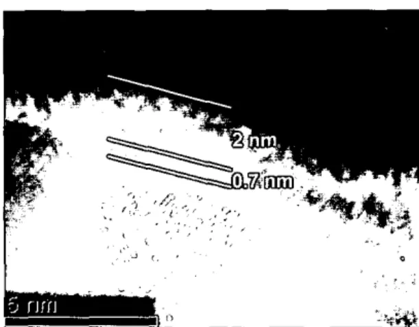
Fig. 1 Cross-section TEM micrograph of H m 2 onp-type Si
wafer, after 300 sec post deposition annealing at 600
"C.
It is clearly observed from the cross-section transmission electron microscopy (TEM) micrograph, as Fig.
1 shows, that -0.7 nm interfacial layer is formed in addition
to the 2nm (physical thickness) H f 0 2 film after 300 sec post deposition annealing at 600
"C.
The capacitance equivalent thickness (CET) is 1.3 nm. Note that the CET value isobtained by two-frequency (500 kHz & 100 kHz) correction method [7]. The CET have constant values before and after hydrogen and deuterium treatment ,indicating that it will not increase the interfacial layer thickness.
There are significantly reductions (more than 3 orders) of current density at inversion bias after post-metallization annealing incorporating deuterium and hydrogen at 400
"C
for 30 min (Fig. 2 and Fig. 3). The little difference of Jg -Vg curves before and after constant voltage stress at -3 V exceed
Gate Voltage (Volt)
J, -Vg curves of H f 0 2 gate stack MIS capacitors Fig. 2
incorporating H2 treatment.
-o-
after
stress
Gate Volt& (Vdt)
Fig. 3 J, -Vg curves of H f 0 2 gate stack MIS capacitors
incorporating Dz treatment.
0-7803-8454-7/04/$20.00 02004 IEEE. 166
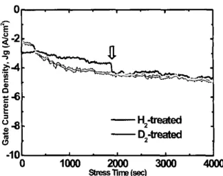
Fig. 4 Time evolutions of gate current of H f 0 2 gate stack MIS capacitors incorporating H2 and D2 treatment under -3 V constant voltage stress.
4000 sec show the good stability of H f 0 2 films after PMA to
incorporate deuterium and hydrogen treatment. Fig. 4 shows the time evolutions of H f 0 2 gate current after H2 and deuterium treatment under constant voltage stress (CVS) at gate voltage (Vg) of -3 volts. Note that the hydrogen-treated device shows the observable gate current discontinuous occurs during the CVS, as compared to the deuterium-treated device (the smoother curve) under the same conditions. The reliability of Pt/Hf02 gate dielectric
stack is effectively enhanced by introducing deuterium treatment PMA at 400
"C
for 30 min, as compared to hydrogen-e-
H2-treated
-n-
D2-treated
fresh
annealing
stress
Fig. 5 Interface trap density of Pt/Hf02 gate stack MISstructure beforeiafter H2 (D2) treatment and after stress,
respectively.
The interface trap density (Dit) at the midgap energy was estimated using the high-low (500 lcHz & 50 Hr)
frequency method (Fig. 5). The Dit values of as-deposited devices are about IO" cm-2ev", and are slightly decreased after deuterium and hydrogen treatment. The Dit value of hydrogen-treated devices increases significantly (one order of magnitude higher) after CVS at -3 V exceed 4000 sec, as compared to the constant Dit of deuterium-treated devices. That is another evidence for deuterium-technology to
provide a better
PVHf02
gate stack reliability improvement.C C U $
0.50
.-
s
E
0.75-
-
1.00
-
z
20.50
-
Yrad
;
\t
-(b)
fresh
" " "stress lime (sec)
higher after the first constant current stress at 100 mA for IO4
sec (the solid circle). After post-metallization annealing was done in forming gas to incorporate hydrogen (H2 I N2=l 1 9 )
at 400
"C
for 30 min, the significantly reductions of current. density is observed (triangle). The inversion current density degrades to high magnitude after another constant current stress at 100 mA for IO4 sec is carried out.The deuterium-treated samples were processed with the same procedure except replacing hydrogen by deuterium. Fig. 8 shows the similar recoverable characteristic of the
deuterium-treated devices.
Fig. 6 Time evolutions of light emission intensity for (a)H2-
and (b)D,-treated devices under constant current stress at
100 mA.
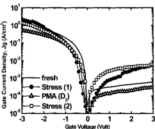
Fig. 7 Recoverable J,.V, curves incorporating H2 treatment
with constant current stress at 100 mA for IO4 sec.
To further investigate the optical characteristic of the
Pt/HfOZ gate stack, the time evolutions of light emission intensity due to the electron-hole plasma recombination is measured [SI. Fig. 6 shows the time evolutions of light
emission intensity for hydrogen-treated and deuterium- treated devices under constant current stress at 100 mA. The fresh devices are initially measured under constant current stress at 100 mA for IO4 sec, followed by the post-metallization annealing in forming gas at 400
"C
for 30 min to incorporate deuterium or hydrogen. As the Fig. 6shows, the normalized light emission intensity of
deuterium-treated device is stable and with less fluctuation
10"
(12.5%) compared to the fresh device (25%). Note that the
hydrogen-treated device shows small gate current
10'
fluctuation at the beginning, and a significantly drop and fluctuation after 5500 sec.
Nz
10'
2
;
1 ~ 1
.$
'
5$
2
3
-2 -10
1a
Voltase ( V 4It is interesting to note that the Jg-Vg characteristic of inversion current regarding to constant current stress with hydrogen and deuterium-treatment are recoverable. As Fig. 7 shown, solid line indicates .I-V, curve o f t h e fresh devices. The inversion current increased 5 orders of magnitude
Fig. 8 Recoverable J,-V, curves incorporating DZ treatment
with constant current stress at 100 mA for IO4 sec.
4. Conclusions
The Pt/HfOZ gate stack reliability is enhanced by introducing deuterium and hydrogen treatment during the post-metallization annealing. For comparison, deuterium -treated technology provides slightly better reliability improvement on both the electrical and optical reliability of
PtfHf02 gate stack devices. Due to the interfacial layers, the results are similar to SiO, gate dielectrics.
Acknowledgments
The HfO, deposition by ASM is highly appreciated
References
[ I ] G . D. Wilk, R. M. Wallace, and J. M. Anthony, “High-k gate
dielectrics: Current status and materials properties considerations”, J. Appl. Phys., vol. 89, pp. 5243-5275,2001. [2] C. Hobbs, H. Tseng, K. Reid, B. Taylor, L. Dip, L. Hebert, R.
Garcia, R. Hegde, I. Grant, D. Gilmer, A. Franke, V.
Dhandapani, M. Azrak, L. Prabhu, R. Rai, S. Bagchi, J. Conner, S. Backer, F. Dumbuya, B. Nguyen, P. Tobin, “80 nm poly-Si gate CMOS with Hf02 gate dielectric”, in IEDMTech.
Dig., 2001, pp. 30.1.1
-
30.1.4.C. Hobbs, L. Fonseca, V. Dhandapani, S. Samavedam, B. Taylor, I. Grant, L. Dip, D. Triyoso, R. Hegde, D. Gilmer, R. Garcia, D. Roan, L. Lovejoy, R. Rai, L. Hehert, H. Tseng, B. White, P. Tobin, “Fermi level pinning at the polySiImetal oxide interface”, in VLSl Tech. Symp., June 2003, pp. 9-10. [4] E. Vainonen-Ahlgren et al. Computational Materials Science,
27, pp. 65-69 Issue: 1-2 (2003).
[5] E. P. Gusev, D. A. Buchanan, E. Cartier, A. Kumar, D. DiMaria, S. Guha,A. Callegari, S. Zafaar, P. C. Jamison, D. A.
Neumayer, M. Copel, M. A. Grihelyuk, H. Okom-Schmidt, C. D’Emic, P. Kozlowski, K. Chan, N. Bojarczuk, L. -A.
Ragnarsson, P. Ronsheim, K. Rim, R. J . Fleming, A. Mocuta,
A. Ajmera, “Ultrathin high-K gate stacks for advanced CMOS devices”, in IEDM Tech. Dig., 200 I , pp. 20.1.1
-
20. I .4.[6] D. Barlage, R. Arghavani, G. Dewey, M . Doczy, B. Doyle, J.
Kavalieros, A. Murthy, B. Roberds, P. Stokley, R. Chau, “High-frequency response of 100 nm integrated CMOS transistors with high-K gate dielectrics”, in IEDM Tech. Dig.,
2001, pp. 10.6.1 - 10.6.4.
[7] K. J. Yang, Chenming Hu, “MOS capacitance measurements for high-leakage thin dielectrics”, IEEE Trans. Electron
Devices, vol.46,no. 7,pp. 1500-1501, 1999.
[8] C. W. Liu, M. -1. Chen, 1. C. Lin, M. H. Lee, and C. -F. Lin, ‘Temperature dependence of the electron-hole-plasma electroluminescence from metal-oxidesilicon tunneling diodes”, Appl. Phys. Lett., vol. 77, pp. 1 I 1 1-1 113, 2000. [3]