A
6MHz-130MHz
DLL with a Fixed Latency
of
One Clock Cycle Delay
Hsiang-Hui Chang, Jyh-Woei Lin, and Shen-Iuan Liu
Department of Electrical Engineering & Graduate Institute of Electronic Engineering, National Taiwan University Taipei, Taiwan 10617, R. 0. C.
Abstract
In this paper, a wide range delay-locked loop (DLL) with a fixed latency of one clock cycle is proposed. Using the phase selection circuit and the start-controlled circuit enlarges the operating frequency range of this DLL and eliminates the harmonic loclung problems. The operating frequency range of the DLL can be from l/T~,,,j,, to l / ( N x T h ) , where T& and TD, are the minimum and maximum delay of a delay cell, respectively, and N is the number of delay cells used in the delay line theoretically. Fabricated in a 0.35-um 1P3M standard CMOS process, the DLL occupies an active area of 880-umx515-um and consumes a maximum power of 132 mW at 130 MHz. The measurement results exhlbit that the operating frequency range is from 6MHz to 130MHz and the latency is just one clock cycle. From the entire operating frequency range, the maximum rms jitter would not exceed 25 PS.
introduction
The rapid and continuous advances of CMOS processes over the past twenty years have led to a highly-integrated level and a fast operation speed in electronic systems. As the system complexity and operation frequency increase, the issue of synchronization becomes of paramount concem since it strongly dominates the system performance. Phase- locked loops (PLLs) [ 11 and Delay-locked loops (DLLs) [2-
31 have been typically employed for the purpose of synchronization. Due to the difference of their configuration, the DLLs are preferred for their unconditional stability and faster locking time than PLLs. Besides, a DLL offers better jitter performance than a PLL because noise in the voltage-controlled delay line (VCDL) does not accumulate over many clock cycles.
Conventional DLLs may suffer from harmonic locking over wide operating range. If the DLLs want to operate at lower frequency without harn.mic locking, the number of delay stages must be increased to let the maximum deiay ofthe delay line equal to the period of the lowest frequency. However, the maximum operating frequency of a DLL will be limited by the minimum delay of the delay line.
If the delay different from an integer of clock periods is detected, the closed loop will automatically correct it by changing the delay time of the VCDL. However, the conventional DLL will fail to lock or falsely lock to two or more periods, Tclk, of the input signal if the initial delay of
the VCDL is shorter than 0.5 Tclk or longer than 1.5 Tclk as
Fig.1 The DLL in normal lock and false lock conditions shown in Fig. 1. Therefore, if the DLL is desired to lock a delay which it is just one clock cycle of input reference signal, the initial delay of VCDL needs to be located between 0.5 Tref and 1.5 Tref no matter what the initial voltage of the loop filter is. If the maximum and minimum delay of the VCDL are T V C D L - ~ ~ and TvcDL-,,~,,, respectively. As a result, the p eriod o f i nput s ignal should satisfy the following inequality [4]:
However, if TVCDL m x 23xTVCDL--, there is no range of TCLK that can satisfy eq. (1) and the DLL is prone to the false locking problem. It is difficult to design a VCDL in which TvCDL-~~ is just e qual t o 2 XTVCDL min when p rocess
variations are taken into account. Thus, some solutions
[4]-[8] have been proposed to overcome this problem. In thls work, an approach using the phase selection circuit to automatically decide what number o f d elay c ells s hould b e used. It can enable the DLL to operate in the wide frequency range Meanwhile, a new start-controlled circuit is presented for the DLL to solve false loclung problems and keep the latency of one clock cycle. Its duty cycle is not necessary to be exact 50%.
a.
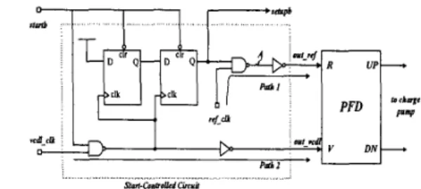
The architecture of the proposedDLL
The architecture of the proposed DLL is shown in Fig. 2. It is composed of a conventional analog DLL, a phase selection circuit and a start-controlled circuit. Before the DLL begins to lock, the phase selection circuit will choose an appropriate delay cell to be a feedback signal (vcdl-clk) according to different frequencies o f input signal. I n other words, the number of the delay cells may change at different input frequencies. The minimum delay, TD-, o f t he delay line is determined by one unit-delay cell. The maximum
4-3-
1
IEEE 2002 CUSTOM INTEGRATED CIRCUITS CONFERENCE
0-7803-7250-6/02/$10.00 0 2002 IEEE
-_
I
Fig.2 System architecture of the proposed DLL
delay is decided by NxTDmax where N is the number of unit- delay cells. Thus, the operating frequency range of the DLL can be from l/TD,,,i,, to l/(NxTD,,). As the input frequency is higher, the phase selection circuit will select the smaller number of delay cells and the gain o f t he V CDL w h c h i s proportional to the number of delay cells will become smaller. In order to have an adequate loop bandwidth for the DLL, the capacitances used in the loop filter must become smaller. In this work, 3-bits control signals generated from the phase selection circuit will switch the number of capacitors in the loop filter depending on the selected phase. After the vcdl-clk is decided, the DLL will start the locking process whch is controlled by the start-controlled circuit. First, the delay between input and output of the VCDL is initially set to the minimum value and then let the down signal of the PFD output activate, supposed that the VCDL's delay increases with control voltage decreasing. Therefore, the delay between input and output of the VCDL will increase until it reaches one clock period of the input signal. Thus, the DLL will not fall into false locking and the latency is fixed to one clock cycle no matter how long delay the VCDL can provide.
III.
Circuit descriptionA. Phase selection circuit
The phase selection circuit consists of two blocks: an edge detector and a multiplexer with a decoder, as shown in Fig.
3. The schematic and timing diagram of the edge detector are shown in Fig. 4 and Fig. 5, respectively. At the initial state, the signal startb is set to low to reset the edge detector outputs (i.e., d3
-
d10) and the delay of the VCDL is set to its minimum value. When the signal startb goes high, the edge detector will detect the rising edge of input signals in sequence during the next two rising edge of ref-clk. Referring to Fig. 5(a), suppose that the signals (phase 3-
phase 10) are all have rising edges in sequence during oneclock cycle, therefore, the outputs (d3
-
d10) are all high and the multiplexer will select the phase 10 as the output signal, vcdl-clk. However, if the input frequency is higher, suppose that the timing diagram is similar to Fig.5 (b). All the inputs have rising edges during one clock cycle, but only the rising edges of phases (1-
4) in sequence lead the selected phase to be 4. The vcdl-clk will be low until the selected phase is chosen. After the vcdl-clk is decided, the DLL will start the locking process, which is explained later. By the decoder, signals (d3-
d10) are decoded to generate 3-bits control signals which switch the number of capacitors used in the loop filter for tuning the loop bandwidth.Fig.3 Block diagram of the phase selection circuit
$
Ldl*$
Id, ...Id,,
b,
flue- 14"
Fig.4 Schematic of the edge detection circuit
.*
-
--
* a - %-* '1111-' 2 -( 0 ) P IFig.5 Timing diagram of the edge detection circuit
control voltage of the loop filter is directly feed to NMOS rather than PMOS. Therefore, the transfer curve of delay vs. control voltage is monotonic decreasing.
I
h.... . ., ...^. ^..,...^....^.... ...,., .. ... .. , ..
slu(-CmbolkdCkxil
Fig. 6 Schematic of start-controlled circuit associated with a PFD
Fig.7 Timing diagram of the start-controlled circuit
B. Start-controlled circuit
The schematic of the start-controlled circuit and the associated PFD are shown in Fig. 6. It composes only of two rising edge trigger DFFs, two NAND gates and two inverters. The timing diagram of this start-controlled circuit is shown in Fig. 7. Initially, startb is set to low in order to clear the two DFFs outputs. Therefore, setupb is low and
pulls the control voltage to VDD as shown in Fig. 3 (i.e., set
the VCDL delay to its minimum value). In this way, the two inputs of the PFD are in low level. When the startb goes to
high, the setupb will also go to high. After two consecutive
falling edges of vcdl-clk trigger the DFFs, the down signal of the PFD will be activated and let the delay of the VCDL increase. The delay of the VCDL will increase until it is equal to one clock period of the input signal due to the nature
of negative feedback architecture. In order to get equal delays for path1 and path2, some dummy loads should be added in point A. In comparison with [5], the start-controlled circuit has two advantages: one is that the proposed circuit is simple and the other is that the duty cycle of ref-clk and vcdl-clk does not require to be exact 50%.
C. Other-circuits
In t l u s work, the dynamic logic style PFD [9] is adopted to avoid the dead zone problem and improve the operating speed. To mitigate charge injection errors induced by the parasitic capacitors of the switches and current source transistors, the charge pump circuit developed in [lo] is used. here. The delay cell circuit is similar to [lo]. The
N.
Measurement results
The prototype chip is fabricated in a 0.35-um single-ploy
triple-metal standard CMOS process and the
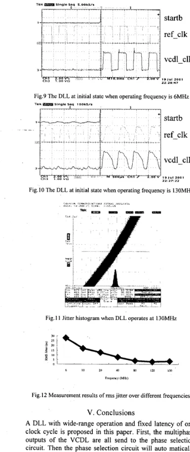
microphotograph of the chip is shown in Fig. 8. The capacitors used in the loop filter are integrated in the chip and formed by metal-to-metal capacitors. The experimental results show that the DLL can operate in the frequency range of 6 MHz
-
130 MHz. Fig. 9 and Fig. 10 show the locking process of the DLL as the operating frequency is 6 MHz and 130 MHz, respectively. From Fig. 9 and Fig. 10, show that the first four cycles of the DLL in the locking process as the operating frequency is 6 MHz and 130 MHz, respectively. After the signal, startb, is high, the phase selection circuit will select one of the outputs of the VCDL as close as possible to the next rising edge of the input clock, ref-ck. Fig. 9 and Fig. 10 also show that after the signal, startb, is high, the first rising edge of the output clock of the VCDL, vcdl-clk, leads that of the input clock, ref-clk. Since the signal, startb, will set the control voltage, Vctrl, in Fig. 2 to Vdd, the proposed phase detector and the current pump circuit will discharge the loop filter to increase the delay of the VCDL. It will align the phases between the input clock and output clock of the VCDL. Fig. 1 1 shows the jitter histogram when DLL operates in 130 MHz. Fig. 12 shows the measurement results of rms jitter over different frequencies. Table I gives the performance summary. As aresult, the proposed DLL indeed have a wide-operational range and a fixed latency of one clock cycle.
Fig.8 Microphotograph of the chip.
startb
ref-clk
Processvcdl-clk
1 9 J U I 2001 22 2s 4 7 3 . ct13 1 0 0 “‘il 0.35-~m 1P3M TSMC CMOS processselect one of the delayed outputs to feedback. As a result, this DLL can operate over the wide range without suffering from harmonic locking problems. Ideally, this DLL can operate from l/(NxTDmax) to I/T,,-. The experimental results also demonstrate the functionality of the proposed DLL. Moreover, at different operating frequencies, the jitter performances are all in an acceptable range and the latency is just one clock cycle.
Operating Voltage
Operating Frequency Range RMS Jitter
Fig.9 The DLL at initial state when operating frequency is 6MHz
Tek single seq 1 ooks/s
3.3
v
6 MHz-
130 MHz 24.77 ps @ 6 MHzstartb
ref-clk
Power Dissipation Active Area f , . . . . , . , , J l S l “ l 2 0 0 1 2 2 2 7 2 2 I t 3 500)1* c n 1 1 2 :E: IFlg.10 The DLL at initial state when operating frequency is I30MHz
24.3-ps
@ 130 MHz
132 mW @, 130 MHz880-umx515-um @ without pads
Fig. 11 Jitter histogram when DLL operates at 130MHz
6 I O 20 40 80 12U 130
Frequerq (Mth)
Fig. 12 Measurement results o f rms jitter over different frequencies
V. Conclusions
A DLL with wide-range operation and fixed latency of one
clock cycle is proposed in this paper. First, the multiphase outputs of the VCDL are all send to the phase selection circuit. Then the phase selection circuit will auto matically
- -
13.297 ps @ 130 MHz
1210 ps @ 6 MHz Peak-to-Peak Jitter
VI. References
[ 11 B. Razavi, “ Monolithic phase-locked loops and clock recovery circuits:
theory and design ”, IEEE press, 1996.
[2] R. L. Aguitar and D. M. Santos, “Multiple target clock distribution with arbitrary delay interconnects,” IEE Electronic Leffers., vol. 34, no. 22, pp. [3] R. B. Watson, Jr. and R. B. Iknaian, “Clock buffer chip with multiple
target automatic skew compensation”, IEEE J. Solid-Stute Circuits, vol. 30, no. 11, pp. 1267-1276, Nov. 1995.
[4] Y. Moon, J. Choi, K. Lee, D. K. Jeong, and M. K. Kim, “An all- analog multiphase delay-locked loop using a replica delay line for wide-range operation and low-jitter performance”, IEEE J. Solid-Sfute Circuits, vol. 35, no. 3, pp. 377-384, Mar. 2000.
[5] C. H. Kim et al, “A 64-Mbit, 64O-Mbytels bidirectional data strobed, double-data-rate SDRAM with a 40“ DLL for a 256-Mbyte memory system”, IEEE J. Solid-Stute Circuifs, vol. 33, no 11, pp. [6] D. J. Foley, and M. P. Flynn, “CMOS DLL-based 2-V 3.2-ps jitter 1-
GHz clock synthesizer and temperature-compensated tunable oscillator”, IEEE J. Solid-Stute Circuits, vol. 36, no. 3, pp. 417-423, Mar. 2001.
[7] H. Yahata, T. Okuda, H. Miyashita, H. Chigasaki, B. Taruishi, T. Akiba, Y. Kawase, T. Tachibana, S. Ueda, S. Aoyama, A. Tsukinori, K. Shibata, M. Horiguchi, Y. Saiki, and Y. Nakagome,” A256-Mb double- data-rate SDRAM with a 10-mW analog DLL circuit”, Symposium on
VLSI Circuits Digest of Technical Papers, pp. 74-75, June 2000. [SI Y. Okuda, M. Horiguchi, and Y Nakagome,” A 66-400 MHz,
adaptive-lock-mode DLL circuit duty-cycle error correction”, Symposium on VLSI Circuits Digest of Technical Papers, pp. 37-38,
June 2001,
[9] S. Kim, et al., “A 960-Mb/s/pin interface for skew-tolerant bus using low jitter P L Y , lEEE J. Solid-Stute Circuits, vol. 32, no 5, pp. 691- 700, May 1997.
[ 101 J. G. Maneatis, “Low-jitter process-independent DLL and PLL based on self-biased techniques”, IEEE J. Solid-Stufe Circuits, vol. 3 1, no 11,
21 19-2120, Oct. 1998.
1703-1710, NOV. 1998.
pp. 1723-1732, NOV. 1996.