A MULTI-BAND MULTI-STANDARD RF
FRONT-END FOR IEEE 802.16a and IEEE 802.11a/b/g
APPLICATIONS
Chao-Shiun Wang, Wei-Chang Li, and
Chorng-Kuang Wang
Graduate Institute of Electronics Engineering & Department of Electrical Engineering National Taiwan University, Taipei, Taiwan
Abstract—This paper presents a multi-band multi-standard
receiver architecture for wireless applications, such as 802.11 a/b/g WLAN, and 802.16a WMAN. The targeted frequency bands include licensed bands – 2.3 GHz, 2.5 ~ 2.7 GHz, and 3.5 ~ 3.7 GHz, and un-licensed bands – ISM 2.4 GHz and U-NII 5 GHz. The main advantages of the proposed receiver are using a single frequency synthesizer to perform entire frequency transferring, and each frequency band shares the identical LNA and mixer to reduce chip area. The maximum hardware
shared LNA and Mixer design are also presented. The S11 of
the proposed multi-band LNA is below -10 dB from 2 GHz to 6 GHz. The integrated NF of the RF-Front-End is 3.18 dB at 2.4 GHz, 3.47 dB at 3.5 GHz, and 5.47 dB at 5.4 GHz. The conversion gain and IIP3 are 35 dB and -16.7 dBm at 2.4 GHz, 34.3 dB and -17.4 dBm at 3.5 GHz, and 30.6 dB and -11.3 dBm at 5 GHz respectively. Using a 0.18µm CMOS process, the multi-mode RF front-end dissipates 56 mW from a 1.8V supply voltage.
I. INTRODUCTION
The wireless market is growing rapidly. Being pushed by market demands, various wireless communication systems are emerging. Wireless local area networks (WLANs) have been introduced in ISM and UNII bands for indoor wireless access. IEEE 802.16a Wireless Metropolitan Area Networks (WMANs) standard [1] published on 1 April 2003 for urban area coverage wireless access as the “last mile” solution. IEEE 802.16a system addresses frequencies from 2 to 11 GHz, including licensed and un-licensed bands while the dominant bands [2] are licensed bands of 2.3 GHz (WCS), 2.5 to 2.7 GHz (MMDS), 3.5 to 3.7 GHz (ETSI), and un-licensed bands of 2.4 GHz (ISM) and 5.8 GHz (U-NII) where WLANs operates as well [3][4].
In order to increase flexibility on the market and functionality of RF transceivers, band and/or multi-standard transceiver architecture solutions are pursued. A straight forward method is to use multi-input stage for each interested frequency. The advantage of the approach is that the performances of each RF front-end can be optimized for
each frequency band, but it suffers from area and cost issues. In this paper, a multi-band multi-standard receiver architecture with maximum hardware sharing for IEEE 802.16a and IEEE 802.11a/b/g is developed. A single wideband input matching LNA and a multi-band down conversion mixer are proposed and implemented to save the chip area and cost.
The paper is organized as following: in section 2, the architecture and the particular frequency plan of receiver for IEEE 802.16a and 802.11a/b/g band and multi-standard applications are proposed. The complete LNA and mixer design considerations are discussed in sections 3 and 4, respectively. The simulation results and performance summary are given in section 5. Finally, conclusions of this design are offered in section 6.
II. RECEIVER ARCHITECTURE
Fig. 1 shows the proposed multi-band multi-standard receiver for IEEE 802.11a/b/g and IEEE 802.16a. Dual-conversion architecture is used for IEEE 802.11a/b/g and IEEE 802.16a. But zero-IF technique is adopted for 3.5~3.7GHz the IEEE 802.16a ETSI band. Since IEEE 802.11b/g, and WCS and MMDS bands of IEEE 802.16a share adjacent frequency bands around 2.4 GHz, the RF filter can be used for these standards. For this band, the first local oscillator (LO) frequency is located at 3.45 to 4.05 GHz to convert the signal to IF band from 1.15 to 1.35 GHz and then the second LO frequency converts it to the baseband. IEEE 802.11a and U-NII band of IEEE 802.16a also share the same frequency band so that the RF filter can be used for these two standards. For the U-NII band, the first LO frequency is placed at 3.85 to 4.37 GHz to convert the signal to 1.282 ~ 1.457 GHz and then the second LO transfers the signal to the baseband. For the ETSI band, the received signal is directly converted to baseband through the first LO.
To maximize the level of the hardware sharing, the LNA is designed for multi-band reception. The mixers can also be
This program is supported by the National Science Council (NSC), Taiwan, R.O.C.
3974
0-7803-8834-8/05/$20.00 ©2005 IEEE.
shared for all the standards because of the wide-band characteristics of the transconductance. The low-pass channel select filters are programmable to change the cutoff frequency corresponding to each standard. To adjust the signal at appropriate level at the input of the ADCs, the gain range of the PGAs is determined considering the sensitivity and maximum input power for each standard. The ADCs are programmable for multi-standards. The digital baseband extracts DC offset level and feeds back to analog baseband through DACs (not shown in this figure) to subtract DC offset. / 3 1.15 – 1.457 GHz 3.45 - 4.37 GHz VCO Mixer LNA LO/2 LO Band Select Filter 2.3 / 2.4-2.485 / 2.5-2.7 GHz 3.5-3.7 GHz 5.13-5.35 / 5.725-5.825GHz 3.45~4.05 GHz 0 GHz 3.85~4.37 GHz 1.15 / 1.2-1.243 / 1.25-1.35 GHz / 3.5-3.7 GHz / 1.282-1.338 / 1.431-1.457 GHz Digital Baseband Gain Control Calibration Channel Select Filter PGA Channel Select Filter PGA 90o 0o ADC ADC / 3 1.15 – 1.457 GHz 3.45 - 4.37 GHz VCO / 3 / 3 1.15 – 1.457 GHz 3.45 - 4.37 GHz VCO Mixer LNA LO/2 LO Band Select Filter 2.3 / 2.4-2.485 / 2.5-2.7 GHz 3.5-3.7 GHz 5.13-5.35 / 5.725-5.825GHz 3.45~4.05 GHz 0 GHz 3.85~4.37 GHz 1.15 / 1.2-1.243 / 1.25-1.35 GHz / 3.5-3.7 GHz / 1.282-1.338 / 1.431-1.457 GHz Digital Baseband Gain Control Calibration Channel Select Filter PGA Channel Select Filter PGA 90o 0o 90o 0o ADC ADC ADC ADC
Fig. 1. Proposed multi-band multi-standard receiver
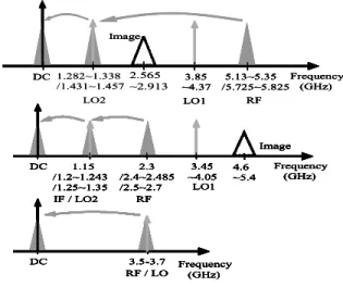
The developed frequency planning of each band is illustrated in Fig. 2. The feature of this architecture is the frequency synthesis for multi-band operation can be achieved by only one voltage control oscillator (VCO) operating from 3.45 to 4.37 GHz, which can be easily implemented by digitally switching binary weighted capacitances in current CMOS technology. In additional, The Local Oscillator 2 (LO2) can be generated by a divide-by-three circuit from the LO1 in this architecture.
Frequency (GHz) DC 3.5-3.7 RF / LO Frequency (GHz) DC Image 2.3 /2.4~2.485 /2.5~2.7 RF IF / LO2 3.45 ~4.05 1.15 /1.2~1.243 /1.25~1.35 LO1 4.6 ~5.4 Frequency (GHz) DC 3.5-3.7 RF / LO Frequency(GHz) DC 3.5-3.7 RF / LO Frequency (GHz) DC Image 2.3 /2.4~2.485 /2.5~2.7 RF IF / LO2 3.45 ~4.05 1.15 /1.2~1.243 /1.25~1.35 LO1 4.6 ~5.4 Frequency (GHz) DC Image 2.3 /2.4~2.485 /2.5~2.7 RF IF / LO2 3.45 ~4.05 1.15 /1.2~1.243 /1.25~1.35 LO1 4.6 ~5.4 Frequency (GHz) DC Image 5.13~5.35 /5.725~5.825 RF LO2 3.85 ~4.37 LO1 Frequency (GHz) DC Image 5.13~5.35 /5.725~5.825 RF 3.85 ~4.37 LO1 2.565 ~2.913 1.282~1.338 /1.431~1.457 Frequency (GHz) DC 3.5-3.7 RF / LO Frequency(GHz) DC 3.5-3.7 RF / LO Frequency (GHz) DC Image 2.3 /2.4~2.485 /2.5~2.7 RF IF / LO2 3.45 ~4.05 1.15 /1.2~1.243 /1.25~1.35 LO1 4.6 ~5.4 Frequency (GHz) DC Image 2.3 /2.4~2.485 /2.5~2.7 RF IF / LO2 3.45 ~4.05 1.15 /1.2~1.243 /1.25~1.35 LO1 4.6 ~5.4 Frequency (GHz) DC 3.5-3.7 RF / LO Frequency(GHz) DC 3.5-3.7 RF / LO Frequency (GHz) DC Image 2.3 /2.4~2.485 /2.5~2.7 RF IF / LO2 3.45 ~4.05 1.15 /1.2~1.243 /1.25~1.35 LO1 4.6 ~5.4 Frequency (GHz) DC Image 2.3 /2.4~2.485 /2.5~2.7 RF IF / LO2 3.45 ~4.05 1.15 /1.2~1.243 /1.25~1.35 LO1 4.6 ~5.4 Frequency (GHz) DC Image 5.13~5.35 /5.725~5.825 RF LO2 3.85 ~4.37 LO1 Frequency (GHz) DC Image 5.13~5.35 /5.725~5.825 RF 3.85 ~4.37 LO1 2.565 ~2.913 1.282~1.338 /1.431~1.457
Fig. 2. Frequency planning III. LNA DESIGN
One of the difficulties in the design of a multi-band application transceiver is how to realize a multi-band LNA. Many LNA topologies for multi-band applications have been
proposed. The most popular method [5] is to use an LNA for each band. The advantage of this approach is that the performances of each LNA can be optimized for each interested band, but this technique may suffer from area and cost issues. The common-gate stage is the other way to realize a wide-band LNA [6]. However, the common-gate topology usually has relative higher noise figure than the previous approach. A concurrent multi-band LNA [7] based on inductor degeneration technique can achieve a relative lower NF, therefore, this topology is usually adopted especially for the systems with less noise figure budget. Thus narrow-band CMOS LNA designs have employed inductive source degeneration technique to achieve good input matching, and yield nearly optimal noise performance at the high operating frequency of the input network.
A. Input Matching
In order to receive the desired frequencies operating at 2.4 GHz, 3.5 GHz and 5.8 GHz, LNA design adopts wide-band input matching topology. In Fig. 3, the input impedance Zin is embedded in 2nd-order band-pass LC-ladder filter to resonate its reactive part over the whole band, from 2 GHz to 6 GHz [8]. For flexibility of the design, an inductor (Lg) is placed in series with the gate, and a capacitor (Cpar) is added in parallel with the gate-source of the amplifying transistor. The cascode configuration improves the reverse isolation and the frequency response of the amplifier. Rs Ls2 =Ls+Lg Cp Lp Cs =Cpar+Cgs Zin Cpar Ls Lg R
Fig. 3. Input matching network using a 2nd-order band-pass LC-ladder
filter
The source degeneration topology synthesizes an input impedance with a real part equal to gmLs/Cp, where Cp =
Cpar+Cgs, to be matched with the source resistance Rs.
B. Band Selection
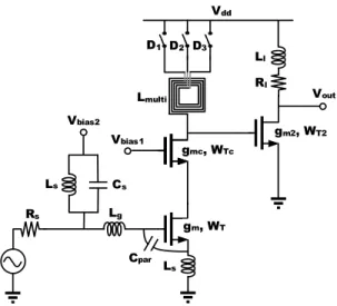
Load inductors, Lmulti as shown in Fig. 4, are switched for the desired band to tune the parasitic capacitor at the output node. To reduce the area occupied by the inductors, they are lumped together using a 5.5-turn spiral inductor with multi-tap. The schematic of the proposed multi-band LNA is shown in Fig. 4. The digital codes of D1D2D3 control the switches for the resonance frequency at each band, namely, for 5 GHz the U-NII band, D1D2D3 = 111, for 3.5 GHz the
ETSI band, D1D2D3 = 011, and D1D2D3 = 001 is for 2.3 GHz (WCS), 2.5~2.7 GHz (MMDS).
Due to the equivalent gate-source capacitor Cp of input device, the gain in 5 GHz band does not satisfy the specification, thus noise figure degrades. The broadband second amplifier stage is intended to solve this problem and relax specification budgets of circuit blocks. The inductance Ll and resistance Rl are designed to achieve that the overall LNA circuit has equal gains in all the frequency bands.
Rs Lg Ls gm, WT gmc, WTc Vdd Vbias1 Vbias2 Cpar D3 D2 D1 gm2, WT2 Ls Cs Lmulti Ll Rl Vout
Fig. 4. Simplified schematic of the proposed multi-band LNA
IV. MIXER DESIGN
Fig. 5 shows the schematic of the proposed dual-conversion mixer. The proposed mixer is composed of a double-balanced Gilbert-type mixer cascaded by two additional double-balance PMOS switching pair. The incoming RF voltage signal is firstly converted into a current signal by transistors M1 and M2 and then multiplied by transistors M3 ~ M6 in current domain to perform frequency translation. The transistors M3 ~ M6 are biased slightly above their threshold voltage. This results in the LO alternately switching M3 (M6) and M4 (M5) on and off. The first Gilbert-type stage translates the 5 GHz (U-NII band) and around 2.4 GHz (WCS, MMDS and ISM bands) signal to IF at 1.15 ~ 1.457 GHz and thus, the spiral inductors, Ll1 and Ll2 , are used as load to amplify the IF signal. Then the IF signal is folded into the two PMOS switching pairs, M7 ~ M14 , to generate the quadrature baseband signals. PMOS has less flicker noise than NMOS does, so it can relax the noise specification budget. The baseband load uses poly resistors, Rl1 ~ Rl4 , due to lacking for flicker noise. For the 3.5 GHz (ETSI band) signal, M4 and M5 are turned off and M3 and M6 are biased as cascoded devices. The second stage down-converts it to baseband signal through LO2 at 3.5GHz. The tank of the load in the first stage resonates at 3.5 GHz when the switch is off; otherwise, the resonance frequency is at 1.3 GHz. LO1 -LO1+ LO1+ LO2i+ LO2i+ LO2i -Vdd Vouti+ Vouti -RFin+ M1 M2 RFin -M3 M4 M5 M6 M7 M8 M9 M10 Ll1 Ll2 Rl1 Rl2 LO2Q -VoutQ -M11 M12 M13 M14 Rl3 Rl4 LO2Q+ LO2Q+ VoutQ+
Fig. 5. Schematic of the proposed dual-conversion mixer
V. SIMULATION RESULTS
The LNA and the mixer are designed in 0.18μm CMOS process using ADS® simulator. The active current of the multi-mode RF front-end is 31 mA from a 1.8 V supply voltage. The S-parameter simulation results of the proposed multi-band LNA are shown in Fig. 6. The insertion loss of each band is below -10 dB between 2 GHz and 6 GHz. The S21 is 14 dB at 2.7 GHz, 13.9 dB at 3.6 GHz, and 13.3 dB at 5.3 GHz.
Fig. 6. Simulations of insertion gain and insertion loss The noise figures (NF) for the three bands of the RF front-end is shown in Fig. 7. The NFs are 3.18 dB at 2.4 GHz, 3.47 dB at 3.5 GHz, 5.47 dB at 5.4 GHz, respectively.
Fig. 7. Noise figure simulations
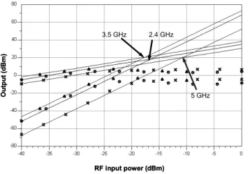
The linearity of the circuit characterized by the overall RF front-end is shown in Figs. 8. The conversion gain and IIP3 of the RF front-end are 35 dB and -16.7 dBm at 2.4GHz,
34.3 dB and -17.4 dBm at 3.5GHz, and 30.6 dB and -11.3 dBm at 5GHz, respectively.
The simulation results for the integrated multi-band RF front-end are summarized in Table 1.
RF input power (dBm) O u tpu t (dBm ) 2.4 GHz 3.5 GHz 5 GHz RF input power (dBm) O u tpu t (dBm ) 2.4 GHz 3.5 GHz 5 GHz
Fig. 8. IIP3 Simulations
Table 1. Performance summary of the RF Front-End simulated LNA Bands (GHz) S21 (dB) NF (dB) (dBm) IIP3 2.4 14 2.3 -15 3.5 13.9 3.2 -10 5.25 13.3 4.4 -1.5 Mixer Bands (GHz) Conversion gain (dB) NFDSB (dB) IIP3 (dBm) 2.4 6.5 15.2 +5.7 3.5 10 14.3 +3.4 5.25 6.0 15.7 +6.24 RF Front-End Bands (GHz) Conversion gain (dB) NF (dB) IIP3 (dBm) 2.4 35.0 3.18 -16.7 3.5 34.3 3.47 -17.4 5.25 30.6 5.47 -11.3 VI. CONCLUSION
A highly integrated multi-band multi-standard receiver with dual-conversion/Zero-IF architecture for IEEE 802.16a and IEEE 802.11a/b/g is proposed. With proposed receiver architecture and frequency plan, only single frequency synthesizer is required for multi-standard application. To maximum the level of component share in the multi-band receiver, the targeted three frequency bands share an LNA and a mixer. The wide input matching LNA with adjustable load has been developed. The wide input folding cascaded mixer is also presented for dual-conversion and Zero-IF architecture. All the circuits and the proposed receiver configuration are suitable for area-efficient multi-band and multi-standard receivers.
REFERENCES
[1] Air Interface for Fixed Broadband Wireless Access Systems-Amendment 2 : Medium Access Control Modifications and Additional Physical Layer Specifications for 2-11 GHz, IEEE std. 802.16a, Part 16, 2003.
[2] Adlane Fellah, “WiMAX, NLOS and Broadband Wireless Access (Sub-11 GHz) Worldwide Market Analysis 2004-2008”, Maravedis Inc., Feb. 2004.
[3] Wireless LAN Medium Access Control (MAC) and Physical Layer (PHY) specifications: Higher-speed Physical Layer Extension in the 2.4-GHz Band, IEEE std. 802.11b, Part 11, Sep. 1999.
[4] Wireless LAN Medium Access Control (MAC) and Physical Layer (PHY) specifications: Higher-speed Physical Layer in the 5-GHz Band, IEEE std. 802.11a, Part 11, Sep. 1999.
[5] Jussi Ryynanen, Kalle Kivekas, et al, “A single chip multimode receiver for GSM 900, DCS1800, PCS1900, and wcdma”, IEEE JSSC April 2003.
[6] Xiang Guan, Ali Hajimiri, “A 24-GHz CMOS Front-End”, IEEE JSSC Feb. 2004.
[7] Hossein Hashemi, Ali Hajimiri, “Concurrent Multiband low-noise amplifiers — theory, design, and applications ” , IEEE MTT transaction, Jan. 2002.
[8] A. Ismail, A. Abidi, “A 3 to 10 GHz LNA Using a Wideband LC-ladder Matching Network”, IEEE ISSCC 2004