Abstract—An all-digital cycle-controlled delay-locked loop (DLL) is presented to achieve wide range operation, fast lock and process immunity. Utilizing the cycle-controlled delay unit, the proposed DLL reuses the delay units to enlarge the operating frequency range rather than cascade a huge number of delay units. Adopting binary search scheme, the two-step successive-ap-proximation-register (SAR) controller ensures the proposed DLL to lock the input clock within 32 clock cycles regardless of input frequencies. The DLL operates in open-loop fashion once lock occurs in order to achieve low jitter operation with small area and low power dissipation. Since the DLL will not track temperature or supply variations once it is in lock, it is best suited for burst mode operation. Given a supplied reference input with 50% duty cycle, the DLL generates an output clock with the duty cycle of nearly 50% over the entire operating frequency range. Fabricated in a 0.18- m CMOS one-poly six-metal (1P6M) technology, the experimental prototype exhibits a wide locking range from 2 to 700 MHz while consuming a maximum power of 23 mW. When the operating frequency is 700 MHz, the measured peak-to-peak jitter and rms jitter is 17.6 ps and 2.0 ps, respectively.
Index Terms—All digital, cycle-controlled delay unit (CCDU), delay-locked loop (DLL), phase-locked loop (PLL), successive-ap-proximation-register (SAR).
I. INTRODUCTION
W
ITH advances in deep-submicron technologies, the demand for high-performance and short time-to-market integrated circuits has dramatically grown recently. Scal-able microprocessor and graphic-processor systems could cost-effectively port to advanced technologies to increase the clocking rate, lower the power dissipations, and reduce design turn-around time. The synchronization among IC modules will become an important issue. Thus, considerable efforts have been focused on high-performance digital interface circuits to communicate with these digital systems.Phase-locked loops (PLLs) [1]–[3] and delay-locked loops (DLLs) [4]–[8] have been widely used in many high-speed mi-croprocessors and memories. If the frequency synthesis is not needed, the DLLs are preferred for their unconditional stability, faster locking time, and better jitter performance [9]. The tra-ditional analog DLL [4], [6]–[8] generally has better jitter and skew performances, but it is process-dependent and needs a long design time. Conversely, the digital DLL can be migrated over different processes. Moreover, with benefits from scaling
Manuscript received April 1, 2004; revised October 9, 2004. This work was supported in part by MediaTek Inc. and the MediaTek Fellowship.
The authors are with the Graduate Institute of Electronics Engineering and Department of Electrical Engineering, National Taiwan University, Taipei, Taiwan 10617, R.O.C. (e-mail: [email protected]).
Digital Object Identifier 10.1109/JSSC.2005.843596
CMOS technologies, the digital DLL has a lower supply voltage and the potential for good power management [10]–[14].
To facilitate the digital DLL [10]–[14] for various clock-gen-eration circuits or phase-alignment circuits, the operating frequency range should be as large as possible to meet different product’s specifications. Furthermore, the wide-range DLL should tolerate wide variations for clock frequency, process, and temperature. The highest operating frequency of a DLL is limited by the bandwidth of a single delay unit while the lowest operating frequency is restricted by the length of delay line. In order to meet the maximum and the minimum speed requirement at the same time, the conventional digital DLL [10]–[14] demands a delay line composed of high-bandwidth delay units. However, to realize such a DLL by a reasonable chip area, the tradeoff between bandwidth of a single delay unit and length of the delay line will substantially limit the ratio of maximum to minimum operating frequency. In this paper, the proposed DLL incorporating with the cycle-controlled delay unit (CCDU) and the two-step successive-approxima-tion-register (SAR) controller achieves both wide range and fast lock operation. This DLL exhibits a wide locking range from 2 to 700 MHz without the limitations mentioned above and achieves an acceptable jitter performance as compared to the conventional analog DLL [8]. The DLL locks the input clock within 32 clock cycles regardless of input frequencies. The DLL operates in open-loop fashion once lock occurs in order to achieve low jitter operation with small area and low power dissipation. Since the DLL will not track temperature or supply variations once it is in lock, it is best suited for burst mode operation. The simulated sensitivity to temperature and supply variations are 1% change in delay value per 1% change in supply voltage ( ) and 0.16% change in delay value per 1 C change in temperature as changes from 90% to 110% and temperature from 40 C to 125 C, respectively.
Compared to the conventional digital DLL, the overall hard-ware complexity can be reduced at a given operating frequency range and timing resolution. This paper is organized as fol-lows. Comparisons between the conventional and proposed dig-ital DLL are discussed in Section II. The architecture of the pro-posed DLL is addressed in Section III. Circuit implementation is described in Section IV. Measurement results are given in Sec-tion V. Finally, the conclusions are given in SecSec-tion VI.
II. COMPARISONSBETWEEN THECONVENTIONAL ANDPROPOSEDDIGITALDLL
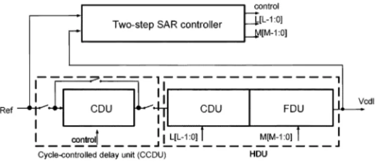
Fig. 1 shows a conventional digital DLL. It consists of three major blocks: a phase detector, a controller, and a digitally con-trolled delay unit, called hierarchical delay unit (HDU).
Fig. 1. Block diagram of the conventional digital DLL.
ally, the HDU can be divided into two parts: one is the coarse delay unit (CDU) and the other is the fine delay unit (FDU). The number of the control bits for the CDU and the FDU is -bits and -bits, respectively. Since the FDU usually inter-polates 1 LSB delay time of the CDU to generate a finer delay, the minimum timing resolution of the FDU could be expressed as
(1) When the DLL locks and the delay time equals to one clock period, the maximum operating frequency range of the conven-tional digital DLL could be expressed as
(2) where is the period of the input clock and is the in-trinsic delay of the conventional digital DLL when all control bits are low. The intrinsic delay is mainly contributed by mul-tiplexers, phase selector, and phase interpolators. As indicated from (1) and (2), the operating frequency range trades off the hardware complexity and the timing resolution. One may either increase or to extend the operating frequency range. How-ever, the former will increase the hardware complexity and the latter will decrease the timing resolution.
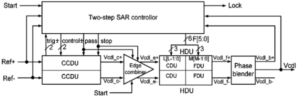
The simplified architecture of the proposed DLL is shown in Fig. 2. It is composed of the CCDU, the two-step SAR con-troller, and the delay line with a CDU and a FDU. The number of the control bits for the CDU and the FDU is -bits and -bits, respectively. The delay units used in the CCDU and the CDU are similar except that the gate length is slightly different. If the initial phase error between Ref and is significantly large, the input clock can reuse delay units in the CCDU to increase the delay time. The maximum cycles that the input clock can circulate in the CCDU are , where is the number of control bits of the programmable counter used in the two-step SAR controller. After the optimum cycles of the CCDU are de-termined, the phase error between Ref and could be fur-ther reduced within one cycle delay of the CCDU. If the total variable delay of the HDU is larger than one cycle delay of the CCDU, the residue phase error could be compensated within 1 LSB delay time of the FDU. Thus, the proposed DLL could
Fig. 2. Simplified architecture of the proposed DLL.
achieve the same timing resolution, , as the conventional dig-ital DLL. Similarly, the maximum operating frequency range of the proposed one could be given as
(3) where is the intrinsic delay of the proposed DLL. If and are slightly different and relatively small, the ratio of the maximum operating frequency range of the proposed DLL to that of the conventional digital one could be approximated as
(4) From (4), the conventional digital DLL should cascade
delay units in the CDU in order to accomplish the same operating frequency range of the proposed one at a given timing resolution. For example, when and , the con-ventional digital DLL requires 2048 delay units in the CDU as shown in Fig. 1. However, the total number of the delay units in the proposed DLL is only 32, which will be explained in Sec-tion IV. Since the hardware complexity of the controller is pro-portional to the operating frequency range, the overall hardware complexity of the proposed DLL could be significantly reduced compared to the conventional digital one at a given operating frequency range and timing resolution. From another view of (4), if , the proposed DLL could improve the operating frequency range by a factor of without decreasing the timing resolution.
Since conventional digital DLLs utilize sequential search scheme to find the optimal value of control bits, the lock time is usually longer than 100 clock cycles [10], [13], [14]. Fur-thermore, the sequential search scheme is not suitable for the wide-range DLL because the initial delay time between input and output clock will be significantly larger or smaller than the period of the input clock in the worst case, resulting in a long lock time. Conversely, the proposed DLL adopting binary search scheme locks the input clock within 32 clock cycles regardless of input frequencies.
III. ARCHITECTURE OF THEPROPOSEDDLL
Fig. 3 is the architecture of the proposed DLL, composed of two CCDUs, an edge combiner, two HDUs, a two-step SAR controller, and a phase blender [15]. In this design, the number
Fig. 3. All digital cycle-controlled DLL.
Fig. 4. Locking procedure of the proposed all-digital DLL.
of control bits for the programmable counter in the two-step SAR controller and the HDU is set to 8-bits and 6-bits, respec-tively. In other words
(5) In order to generate an output with 50% duty cycle, a dual struc-ture, as reported in [13]–[15], is adopted and a pair of comple-mentary inputs, and , with a phase shift of 180 de-grees is required. If the inputs are differential rather than com-plementary, the DLL merely preserves the input duty cycle. The locking procedure is illustrated in Fig. 4. After Start goes high, the initialization will take two cycles. In the cycle-tuning mode, the two-step SAR controller will block into the DLL for power saving and keep constant. The controller will ad-just the value of corresponding to the phase relationship between and the feedback clock, , once every two clock cycles [16], [17]. If the initial delay time between and is relatively smaller than the period of the input clock, the proposed DLL can reuse delay units in the CCDU to increase the delay time. After 16 cycles, the phase error be-tween and could be reduced within one cycle delay of the CCDU and Stop will go high. The locking proce-dure will move to the switching mode, which takes two clock cycles. Meanwhile, the controller will let enter the DLL for generating an output with 50% duty cycle. In the phase-ad-justing mode, the DLL will align the phase of to
within 1 LSB delay time of the FDL by adapting the value of [16], [17]. Since the phase adjustment requires 12 cycles, the total lock time of the proposed DLL is equal to cycles regardless of input frequen-cies. After Lock becomes high, and will be fixed. Therefore, the assertion of lock freezes the delay value setting, so that the DLL then becomes sensitive to supply and temper-ature variations. However, such open-loop design obviates the demand for a dither or lock detector, and hence lowers the power dissipation. is generated by blending itself to match the delay time from to [10], [15].
If the total variable delay of the HDU is larger than one cycle delay of the CCDU, the proposed DLL can improve the op-erating frequency range by a factor of without decreasing timing resolution theoretically. Moreover, the proposed DLL can provide an output, , with the duty cycle of 50%. At the slow–slow process corner with temperature of 100 C, the sim-ulated results indicate and are around 1 ns and 28 ps, respectively. According to (3), the operating frequency range of the proposed DLL can be estimated to be from 2.21 MHz to 1 GHz.
IV. CIRCUITIMPLEMENTATION
A. Cycle-Controlled Delay Unit (CCDU)
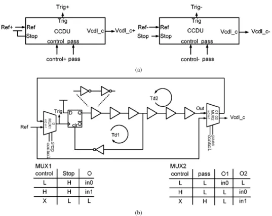
Fig. 5 shows the schematic of the CCDU. Each CCDU is composed of two multiplexers, 13 inverters, and one DFF. The
(b) Fig. 5. (a) Block diagram of the CCDUs. (b) Schematic of the CCDU.
Fig. 6. Timing diagram of the CCDU.
basic operation principle is similar to [18] and [19]. The timing diagram is illustrated in Fig. 6. , generated from the two-step SAR controller, will control the multiplexers to select or the delayed signals, , into the delay line. Once the signals propagate the CCDU, will be triggered to make the programmable counter count upward. will be high until the output of the programmable counter is equal to that of 8-bit SAR register, which will be explained in the next subsection. As shown in Fig. 6, since Td2 is larger than Td1, the delay time between and can be digitally adjusted. It allows the input clock to circulate in the CCDU according to different input frequencies. The delay time between and
can be expressed as
(6) where is the times that the CCDU is reused. The delay time of the CCDU can be increased by reusing the delay units rather than cascading extra delay units.
The undesired duty cycle distortion of the delay line may cause the disappearance of in the low-frequency oper-ation due to mismatches of the driving capability of NMOS and
PMOS in the CCDU. To resolve the problem, the edge-triggered DFF is placed in the front of the delay line so that it only re-sponds to input edges. When the input frequency is high enough to make pass go high, will directly bypass the CCDU. In this case, the optimal cycle of the CCDU is 0. The operation of the other CCDU is the same except that Stop will block into the CCDU for power saving in the cycle-tuning mode.
B. Hierarchical Delay Unit (HDU)
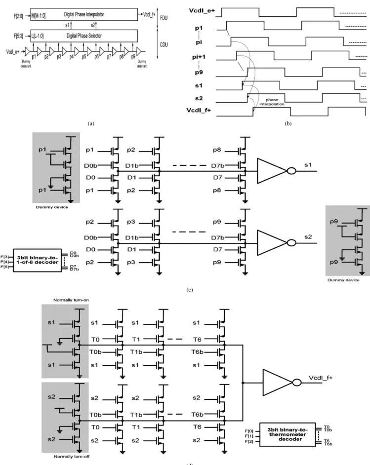
Assuming the total variable delay of the HDU is larger than one cycle delay of the CCDU, the HDU can further compensate the residue phase error between and within 1 LSB delay time of the FDU. A fully digital HDU has been imple-mented by adopting the inverter-base structure of the digital phase selector, the digital interpolator, and the 10-stage delay line as shown in Fig. 7. The dummy delay units are inserted in the first and last stage of the delay line to match the loading of each delay stages. Thus, the total number of delay units in the
proposed DLL is only .
The digital phase selector will choose the two adjacent phases from – , according to the value of . Using the struc-ture of the two-level inverter stage and the 3-bit binary-to-1-of-8 decoder reduces the latency of the digital phase selector as com-pared to the tree structure [20]. The first level inverter stage is composed of eight equal-sized parallel sets. Similarly, the dummy devices are added to compensate the unbalanced par-asitcs in the digital phase selector.
The digital phase interpolator will adjust the output phase of by mixing and , with a weight factor of , determined from the value of . Normally turn-on and turn-off devices could be added in the upper and lower part of the digital phase interpolator, respectively, to improve the
(a) (b)
(c)
(d)
Fig. 7. (a) Block diagram of the HDU. (b) Timing diagram of the HDU. (c) Schematic of the digital phase selector. (d) Schematic of the digital phase interpolator.
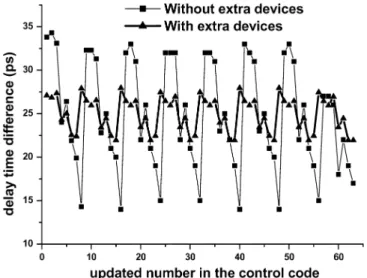
linearity of the characteristic of the HDU. At the slow–slow process corner with temperature of 100 C, the simulated char-acteristic of the HDU is indicated in the Fig. 8. Without the extra
devices, for example, when the value of is switched from 000111 to 001000, the increased delay time of the HDU is rela-tively small, resulting in a larger jump in next phase adjustment.
Fig. 8. Simulated characteristic of the HDU at slow-slow process corner with temperature of 100 C.
The timing resolution of the HDU is less than 28 ps and the total variable delay of the HDU is larger than one cycle delay of the CCDU.
C. Two-Step SAR Controller
Adopting binary search scheme, the two-step SAR controller can provide a fixed lock time of 32 clock cycles over the entire operating frequency range. It is composed of two initialization circuits [8], two phase detectors, 8-bit and 6-bit SAR registers [16], [17], two 8-bit programmable counters, and two control logics as shown in Fig. 9. The outputs of the 8-bit programmable counter, , triggered by , will be compared with that of the 8-bit SAR register, , to decide the state of . The optimal cycles of the CCDU are determined se-quentially one bit per adjustment from the MSB of in the cycle-tuning mode. For example, in the first adjustment, the value of and is set to the initial value, respectively, as shown in Fig. 9. After the input clock circulates 128 times in the CCDU, the counter will reach its final value and
will select as the output of the CCDU, . If the pe-riod of is larger than the delay of the DLL, the rising edge of will lead that of and the MSB of will remain 1, vice versa. Since the duty cycle of is not 50% and the initial delay time between and may be out of the normal operating range [7] for a simple phase detector, the initialization circuit [8] and the edge-triggered phase detector are required. Fig. 10 shows the schematic and the timing dia-gram of the edge-triggered phase detector, . In order to have enough response time for the CCDU, the input frequency is divided by two. A DFF is placed in the signal path of
to match the Clock-to- delay. Some dummy devices, which are not shown in the Fig. 9, are added to balance the loading of each node in the controller.
After Stop goes high, the controller will enter the switching mode and phase-adjusting mode sequentially. In the phase-ad-justing mode, the DLL will align the phase of to within 1 LSB delay time of the FDL by changing the value of
(a)
(b)
Fig. 9. (a) Block diagram of the two-step SAR controller. (b) Example of the timing diagram of the two-step SAR controller.
(a)
(b)
Fig. 10. (a) Schematic of the phase detector(PD C). (b) Timing diagram of the phase detector(PD C).
once every two clock cycles. Thus, the two-step SAR controller ensures the proposed DLL to lock the input clock within 32 clock cycles regardless of input frequencies.
(a)
(b)
(c)
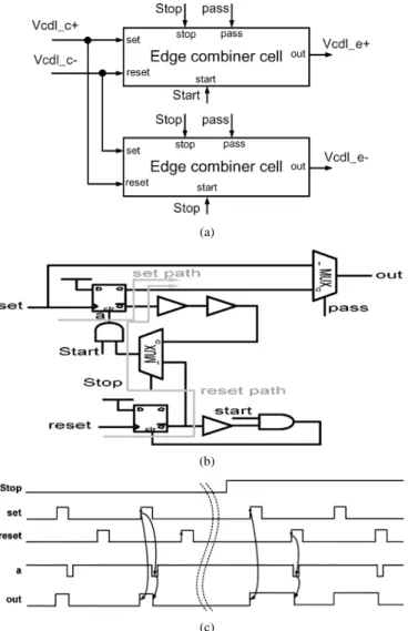
Fig. 11. (a) Block diagram of the edge combiner. (b) Schematic of the edge combiner cell. (c) Timing diagram of the edge combiner cell.
D. Edge Combiner
For the convenience of following signal processing, the duty cycle of and should be recovered to nearly 50%. The schematic and timing diagram of the edge combiner is depicted in Fig. 11. In the cycle-tuning mode, only the upper counterpart is activated to save the power dissipations. Fig. 12 illustrates how the proposed DLL can generate an output with 50% duty cycle. After Stop goes high, is then allowed to enter the DLL. The edge combiner will start to recover the duty cycle of to nearly 50%. The rising edge of is set by that of while the falling edge of is reset by the rising edge of . The operation of the other counterpart is similar but opposite. Assume that both paths consisting of CCDUs, the edge-combiner cells, CDUs, and FDUs are matched. and will be complementary clocks. Incorporating with the phase blender [15], an output with 50% duty cycle is thus generated. If the signal “pass” is high, and will directly bypass the edge combiner. The reason that the duty cycle of and slightly deviating from 50% is caused by the unmatched propagation time be-tween the set and reset path as shown in Fig. 11. However, this error could be corrected by using the phase blender [15].
Fig. 12. Time diagram of generating a 50% duty cycle output.
Fig. 13. Microphotograph of the chip.
V. EXPERIMENTALRESULTS
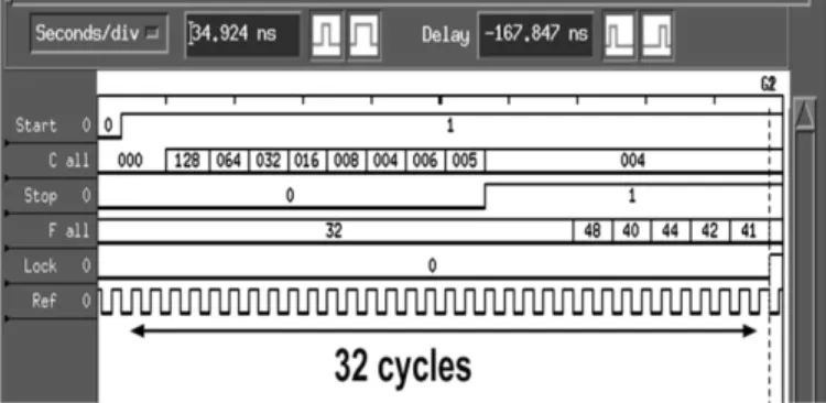
Fig. 13 shows the die microphotograph. The experimental prototype has been fabricated in a 0.18- m one-poly six-metal (1P6M) CMOS technology and occupies a chip area of 1.5 1.5 mm including I/O interfaces. The active area is 0.8 1.1 mm . As indicated from the measured results, the proposed DLL can operate from 2 to 700 MHz at the supply voltage of 1.8 V. Figs. 14 and 15 show the DLL in the locked state when the input clock is 2 and 700 MHz, respectively. The highest operating frequency is limited by the circuit operating speed while the lowest operating frequency is restricted by maximum cycles that the input clock can circulate in the CCDU. Fig. 16 shows the locking procedure, measured by the Agilent Logic Analysis System 16702B, at 100 MHz. After Start goes high, the DLL begins to lock the input clock by adjusting sequentially the value of and and achieves the
Fig. 14. Locked state of the DLL at 2 MHz.
Fig. 15. Locked state of the DLL at 700 MHz.
Fig. 16. Locking process of the DLL at 100 MHz.
locked state within 32 clock cycles. Figs. 17 and 18 show the measured jitter histogram when the DLL operates at 2 MHz and 700 MHz, respectively. When the input frequency is 700 MHz, the measured rms and peak-to-peak jitter is 2.02 ps and 17.6 ps, respectively. Fig. 19 shows the measured results of the jitters and the duty cycle of output clock over different operating frequencies. From Fig. 19, the proposed DLL exhibits a relative jitter performance as compared to the conventional analog DLL [8]. The duty cycle of output clock varies less than 2%. Since the number of cycle times of the CCDU is proportional to the period of the input clock, the clock propagation path will be longer in the low-frequency operation. Thus, the absolute jitters in low frequency are worse than those in high frequency.
Fig. 17. Measured jitter histogram when the DLL operates at 2 MHz.
Fig. 18. Measured jitter histogram when the DLL operates at 700 MHz.
Fig. 19. Measured jitters and the duty cycle of output clock.
But the jitters normalized by the period of the input clock are relatively small. Table I gives the performance summary of the proposed DLL.
VI. CONCLUSION
A wide-range and fast-locking all-digital DLL is presented in this paper. The CCDU enlarges the operating frequency range of the proposed DLL by a factor of without decreasing timing resolution. The two-step SAR controller ensures the DLL to lock the input clock within 32 clock cycles regardless of the input frequencies. The DLL operates in open-loop fashion once lock occurs in order to achieve low jitter operation with small area and low power dissipation. Since the DLL will not track temperature or supply variations once it is in lock, it is best suited for burst mode operation. Given a supplied reference input with 50% duty cycle, the DLL generates an output clock with the duty cycle of nearly 50% over the entire operating frequency range and achieves an acceptable jitter performance as compared to a conventional analog DLL [8]. The proposed all-digital DLL is suitable for the advanced deep-submicron technologies. If more advanced technologies were used, the performance of the DLL such as operating frequency range and jitters could be improved with a little design effort. The power consumption and the total die area would be reduced as well.
ACKNOWLEDGMENT
The authors would like to thank National Chip Implementa-tion Center, Taiwan, for chip implementaImplementa-tion.
REFERENCES
[1] B. Razavi, Monolithic Phase-Locked Loops and Clock Recovery
Cir-cuits: Theory and Design. New York: IEEE Press, 1996.
[2] F. M. Gardner, “Charge-pump phase-lock loops,” IEEE Trans.
Commun., vol. COM-28, no. 11, pp. 1849–1858, Nov. 1980.
[3] R. E. Best, Phase-Locked Loops: Theory, Design and
Applica-tions. New York: McGraw-Hill, 1998.
[4] R. L. Aguitar and D. M. Santos, “Multiple target clock distribution with arbitrary delay interconnects,” Electron. Lett., vol. 34, pp. 2119–2120, Oct. 1998.
[5] R. B. Watson Jr. and R. B. Iknaian, “Clock buffer chip with multiple target automatic skew compensation,” IEEE J. Solid-State Circuits, vol. 30, no. 11, pp. 1267–1276, Nov. 1995.
[6] C. H. Kim, J. H. Lee, J. B. Lee, B. S. Kim, C. S. Park, S. B. Lee, S. Y. Lee, C. W. Park, J. G. Roh, H. S. Nam, D. Y. Kim, D. Y. Lee, T. S. Jung, H. Yoon, and S. I. Cho, “A 64-Mbit, 640-Mbyte/s bidirectional data strobed, double-data-rate SDRAM with a 40-mW DLL for a 256-Mbyte memory system,” IEEE J. Solid-State Circuits, vol. 33, no. 11, pp. 1703–1710, Nov. 1998.
[7] Y. Moon, J. Choi, K. Lee, D. K. Jeong, and M. K. Kim, “An all-analog multiphase delay-locked loop using a replica delay line for wide-range operation and low-jitter performance,” IEEE J. Solid-State Circuits, vol. 35, no. 3, pp. 377–384, Mar. 2000.
[8] H.-H. Chang, J.-W. Lin, C.-Y. Yang, and S.-I. Liu, “A wide-range delay-locked loop with a fixed latency of one clock cycle,” IEEE J. Solid-State
Circuits, vol. 37, no. 8, pp. 1021–1027, Aug. 2002.
[9] M.-J. E. Lee, W. J. Dally, T. Greer, H.-T. Ng, R. Farjad-Rad, J. Poulton, and R. Senthinathan, “Jitter transfer characteristics of delay-locked loops-theories and design techniques,” IEEE J. Solid-State Circuits, vol. 38, no. 4, pp. 614–621, Apr. 2003.
[10] B. W. Garlepp, K. S. Donnelly, J. Kim, P. S. Chau, J. L. Zerbe, C. Huang, C. V. Tran, C. L. Portmann, D. Stark, Y.-F. Chan, T. H. Lee, and M. A. Horowitz, “A portable digital DLL for high-speed CMOS interface circuits,” IEEE J. Solid-State Circuits, vol. 34, no. 5, pp. 632–644, May 1999.
[11] K. Minami, M. Mizuno, H. Yamaguchi, T. Nakano, Y. Matsushima, Y. Sumi, T. Sato, H. Yamashida, and M. Yamashina, “A 1 GHz portable dig-ital delay-locked loop with infinite phase capture ranges,” in IEEE Int.
Solid-State Circuits Conf. Dig. Tech. Papers, Feb. 2000, pp. 350–351.
[12] J.-B. Lee, K.-H. Kim, C. Yoo, S. Lee, O.-G. Na, C.-Y. Lee, H.-Y. Song, J.-S. Lee, Z.-H. Lee, K.-W. Yeom, H.-J. Chung, I.-W. Seo, M.-S. Chae, Y.-H. Choi, and S.-I. Cho, “Digitally-controlled DLL and I/O circuits for 500 Mb/s/pin2 16 DDR SDRAM,” in IEEE Int. Solid-State Circuits
Conf. Dig. Tech. Papers, vol. 431, Feb. 2001, pp. 68–69.
[13] T. Matano, Y. Takai, T. Takahashi, Y. Sakito, I. Fujii, Y. Takaishi, H. Fujisawa, S. Kubouchi, S. Narui, K. Arai, M. Morino, M. Nakamura, S. Miyatake, T. Sekiguchi, and K. Koyama, “A 1-Gb/s/pin 512-Mb DDRII SDRAM using a digital DLL and a slew-rate-controlled output buffer,”
IEEE J. Solid-State Circuits, vol. 38, no. 5, pp. 762–768, May 2003.
[14] J.-T. Kwak, C.-K. Kwon, K.-W. Kim, S.-H. Lee, and J.-S. Kih, “Low cost high performance register-controlled digital DLL for 1 Gbps2 32 DDR SDRAM,” in Symp. VLSI Circuits Dig. Tech. Papers, 2003, pp. 283–284.
[15] K. Nakamura, M. Fukaishi, Y. Hirota, Y. Nakazawa, and M. Yot-suyanagi, “A CMOS 50% duty cycle repeater using complementary phase blending,” in Symp. VLSI Circuits Dig. Tech. Papers, 2000, pp. 48–49.
1994, pp. 298–299.
[20] A. Momtaz, C. Jun, M. Caresosa, A. Hairapetian, D. Chung, K. Vakilian, M. Green, T. Wee-Guan, J. Keh-Chee, I. Fujimori, and C. Yijun, “A fully integrated SONET OC-48 transceiver in standard CMOS,” IEEE
J. Solid-State Circuits, vol. 36, no. 12, pp. 1964–1973, Dec. 2001.
Hsiang-Hui Chang (S’01) was born in Taipei,
Taiwan, R.O.C., on February 4, 1975. He received the B.S., M.S., and Ph.D. degrees in electrical engi-neering from National Taiwan University, Taipei, in 1999, 2001, and 2004, respectively.
His research interests are PLL, DLL, and high-speed interfaces for gigabit transceivers.
circuits and systems.
Dr. Liu received the Engineering Paper Award from the Chinese Institute of Engineers in 2003, the Young Professor Teaching Award from MXIC Inc., the Research Achievement Award from NTU, and the Outstanding Research Award from National Science Council in 2004. He has served as Chair of the IEEE SSCS Taipei Chapter since 2004. He has served as General Chair of the 15th VLSI Design/CAD Symposium, Taiwan, 2004, and as Program Co-Chair of the Fourth IEEE Asia-Pacific Conference on Advanced System Integrated Circuits, Japan, 2004.