行政院國家科學委員會專題研究計畫 期中進度報告
總計劃(1/3)
計畫類別: 整合型計畫 計畫編號: NSC91-2218-E-009-008- 執行期間: 91 年 08 月 01 日至 92 年 07 月 31 日 執行單位: 國立交通大學電子工程研究所 計畫主持人: 任建葳 共同主持人: 李鎮宜,黃家齊,周景揚,陳紹基 計畫參與人員: 李坤儐、張彥中 報告類型: 完整報告 處理方式: 本計畫可公開查詢中 華 民 國 92 年 5 月 26 日
行政院國家科學委員會補助專題研究計畫
□ 成 果 報
告 ■期
中進度
報
告
用於軟體無線電基頻處理之系統晶片設計技術-總計畫
(1/3)
計畫類別:□ 個別型計畫 ■ 整合型計畫
計畫編號:NSC 91-2218-E-009-008
執行期間:91 年 8 月 1 日至 92 年 7 月 31 日
計畫主持人:任建葳
共同主持人:李鎮宜、周景揚、陳紹基、黃家齊
計畫參與人員: 李坤儐、張彥中
成果報告類型(依經費核定清單規定繳交):□精簡報告 ■完整報告
一、總計畫: 用於軟體無線電基頻處理之系統晶片設計技術-總計畫(1/3) 計畫編號:NSC 91-2218-E-009-008 二、子計畫一: 以 OFDM 為基礎之 DAB 與 DVB-T 系統整合型接收機架構設計 (1/3) 計畫編號:NSC 91-2218-E-009-009 三、子計畫二: 以正交分頻多工為基礎之多模式基頻收發機研製(1/3) 計畫編號:NSC 91-2218-E-009-010 四、子計畫三: 數位訊號處理器與可重置加速器之設計(1/3) 計畫編號:NSC 91-2218-E-009-011 五、子計畫四: OFDM FFT 架構下軟體無線電訊處理之軟、硬體輔成設計及其數 附件一位通信之應用設計(1/3) 計畫編號:NSC 91-2218-E-009-012 六、子計畫五: 針對無線通訊上佈局驅動的資料路徑合成器之研究(1/3) 計畫編號:NSC 91-2218-E-009-013
執行單位:國立交通大學電子工程研究所
國立交通大學電信工程學系
中 華 民 國 92 年 5 月 22 日
中文摘要
本研究計畫的目的在設計適合 DAB 與 DVB-T 兩標準之廣播無線電系統 — DXB — 的軟體無線電基頻處理系統單晶片。計畫目標是發展下列關鍵技術:可重置性軟 體無線電架構平台、SoC 系統層次設計技術、高性能、低功耗矽智財設計、SoC 邏輯與實體合成設計、SoC 整合設計與設計流程。第一年完成了 DXB 系統架構、 驗證計畫與系統層次的驗證環境。此外我們也完成了 DXB 所需的關鍵模組與技 術:(1)具單指令多資料(SIMD)及可變長度之 VLIW 能力的高效能、高指令密度的 數位訊號處理器架構與指令集模擬器、(2)低記憶體需求與可變長度的快速傅利 葉轉換處理器、(3) 由誤差大小來決定硬體,並以時間為考量繞線和電路配置 (placement)的自動乘法產生器。 關鍵詞:軟體無線電基頻處理系統單晶片、SoC 整合設計與設計流程、數位訊號 處理器、指令集模擬器、快速傅利葉轉換處理器、乘法產生器。Abstract
This project is to design a dual mode DXB software-defined radio (SDR) baseband system-on-a-chip (SoC) for the two standards DAB and DVB-T. The goals are to develop the following technologies in three years: configurable architecture platform of SDR, SoC system-level design, high-performance low-power silicon IPs, combined
logic-level and physical-level synthesis, SoC integrated design and verification flow. In this year, the general project has outlined the design and verification flow of DXB. In addition, the associative five subjects have completed the following key modules and technologies: (1) design of the architecture and instruction set simulator (ISS) for a high performance, high code density, variable-length VLIW DSP with SIMD capability, (2) Low-memory requirement and variable-length FFT processors, (3) an automatic error-controlled hardware-configurable multiplier generator with timing driven routing and placement considerations.
Keyword: Software-defined radio (SDR) baseband SoC, SoC integrated design and
verification flow, DSP, instruction set simulator, FFT processor, multiplier generator.
1. 簡介
通訊技術的發展,為目前各國家與各公司積極推動的項目,其中又以支援 multiservice、multistadard、multiband 的高速資料傳輸無線通訊為前瞻技術
的主流。例如 IMT-2000 的系統家族觀念(FSC, Family of Systems Concept),
就規定一些共通性的技術規範,以兼容並蓄各種不同的系統標準。因此,不論對 系統設備供應商或是終端設備製造商而言,如何能提供支援多模系統的解決方 案,將會是未來研發技術的重心。軟體無線電技術所欲發展的高彈性軟、硬體系 統平台與正交分頻多工傳輸所提供的高速資料傳輸,正是提供多模系統解決方案 的關鍵技術,因此成為許多大型計畫的重點研發項目,包括政府積極推動的矽導
計 畫 與 歐 洲 的 IST(Information Society Technologies,
http://www.ist-mind.org/) 計畫等等。預計 2005 年時,全球將會有應用軟體 無線電技術之相關產品,而在 2010 年時更是軟體無線電大放異彩的時候。 本研究計畫的目的在發展適合數位音響廣播系統(以下簡稱 DAB)與數位影 像廣播地面廣播系統(以下簡稱 DVB-T)兩標準之廣播無線電系統 — DXB — 的 軟體無線電基頻處理系統單晶片。DAB 與 DVB-T 之運作有甚多相似之處,因此可 將這些功能做適當參數化的設計,即可達到硬體共用之目的;而在不共用的功能 可由軟體實現或軟體控制專屬硬體來運作。由此方式可達到軟體定義無線電 (SDR)之應用。由圖 1可以清楚看到 DXB 系統共用的部份,在不同的運算方式 則區分為不同處理路徑,而對應到的軟、硬體平台則如圖 2 所示。DXB 不但系統 設計本身複雜,所研究的技術更含括軟體、硬體、設計自動化等,因此完善的設 計、驗證與整合規劃更形重要,才能夠讓研究人員有效率的研究、發展各自負責 區塊的細部功能與行為。 本總計畫期中報告主要內容分兩部份。第一部份我們將描述我們在總計畫工 作中所規劃和擬採用的 SoC 設計驗證流程,其中包括各階層驗證方法與所採用的 設計平台工具。第二部份包括五個子計畫在第一年執行到目前為止之工作中英文
摘要,至於詳細內容請參考各子計畫之個別報告。 Front End A/D Guard Interval Removal Symbol Timing &
Fractional Frequency Offset Detection FFT Inner De-interleaving Inner Decoding (Viterbi Decoding) Outer De-interleaving Outer Decoding (R-S Decodeing) Demultiplexing and Source Decoding Frame Synchronization by Using Null Symbol
DVB-T DAB DAB DVB-T Mode Detector One-Tap Equalizer Frame Synchronization Integral Frequency Offset Detection Integral Frequency Offset Detection Channel Estimation DVB-T DAB Symbol-by-Symbol Differential Detection Data Detection 圖 1. DXB 接收機系統之功能區塊圖 ARM922T DSP Configurable accelator DAB IP DVB-T IP Memory AMBA User Interface Protocol PHY API RTOS HAL Software Modem Hardware platform Software platform 圖 2. DXB 接收機系統之軟、硬體平台
2. 設計驗證流程
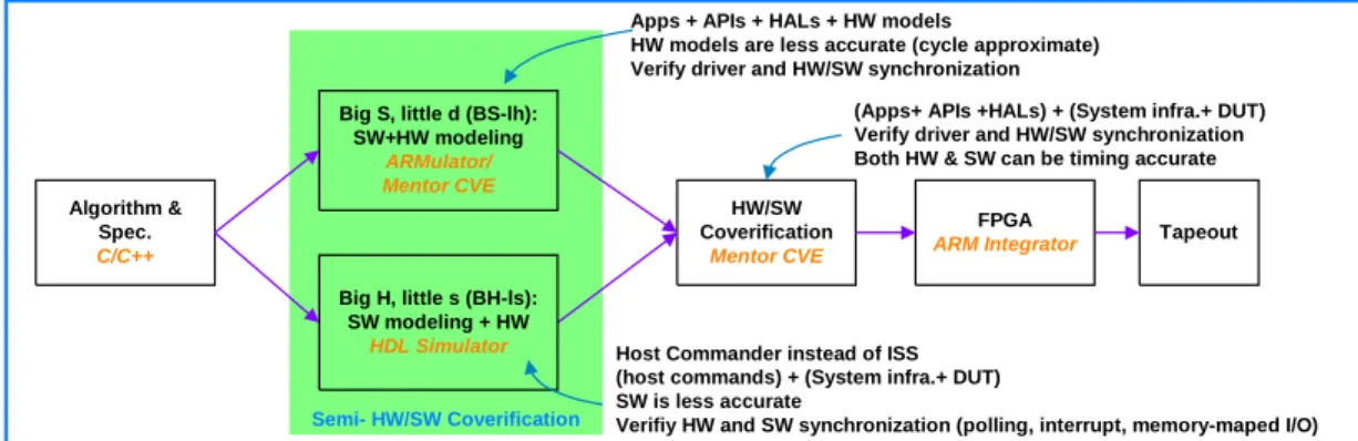
我們採用的是平台式設計驗證流程,如圖 3。平台式驗證流程的主要想法是上一 階段的驗證環境盡量與下一階段的環境相同,因此驗證環境裡的驗證元件需要具 有多個 level 的抽象層,如圖 4。這樣的作法可以盡早達到軟硬體共同設計與驗 證階段,也可減少驗證環境遷移時所要花費的心力。此外,由於是採平台式的設 計(platform-based design)方法學, 所建立的模型 都可在 未來衍生 性設計 (derivative design)中重複使用。圖 3 中: Algorithm & spec.的階段使用 untimed functional model
在以軟體為主(Big Software – little hardware, BS-lh)的驗證環境,是 使用 virtual prototyping
在以硬體為主(Big Hardware – little software, BH-ls)的驗證環境,是 使用 AMBA bus functional model
在 HW/SW coverification 時,結合了 ARM Example of ARM System 裡的系 統週邊與 Mentor Seamless XRAY ARM ISS。
在 FPGA 驗證時,採用 ARM Integrator 這套 rapid prototyping 系統
最後是 tape out 所需的 physical verification
Algorithm & Spec. C/C++ Big S, little d (BS-lh): SW+HW modeling ARMulator/ Mentor CVE Semi- HW/SW Coverification HW/SW Coverification Mentor CVE FPGA
ARM Integrator Tapeout
Big H, little s (BH-ls): SW modeling + HW
HDL Simulator
Apps + APIs + HALs + HW models
HW models are less accurate (cycle approximate) Verify driver and HW/SW synchronization
Host Commander instead of ISS (host commands) + (System infra.+ DUT) SW is less accurate
Verifiy HW and SW synchronization (polling, interrupt, memory-maped I/O) (Apps+ APIs +HALs) + (System infra.+ DUT) Verify driver and HW/SW synchronization Both HW & SW can be timing accurate
ISS ISS +BFM BS-lh Coverification HW/SW Coverification
Application-specific IP, e.g., JPEG encoder, MPEG4 Shape Encoder
Mmeory Organization, e.g., Cache, SRAM, ROM, SDRAM
Basic System Peripherals, e.g., timer, interrupt controller, DMA
Bus Infrastructure, e.g., Arbiter, Decoder, Bridge Standard I/O, e.g., UART, GPIO
Os, Driver, API, HAL
Application Programs, e.g., JPEG encoder
Performance Moniter, e.g., Profiler, Stack Tracker Protocol Moniter, e.g., Bus protocol checker External Model, e.g., UART external model, off-chip memory commander BH-ls Coverification FPGA HW/SW Coverification 圖 4. 平台式驗證裡軟硬體共同驗證環境所函蓋的驗證元件。
2.1 演算法的驗證
無線電應用與一般應用最大不同的地方在於資料傳遞的通道(channel)會隨使用 環境而有所不同,因此 DXB 系統模擬平台必須能夠種模擬現實環境的效應,例如 多重路徑模組(multipath fading channel) 時變杜普勒效應模組(time variant Doppler Effect) 發射接收端無線電頻率偏移效應(CFO)
基頻系統之時脈偏移效應(Clock offset)
此外,如何在混和的效應中清楚地分辨出各種效應對於資料傳輸的影響,與 無線電接收端的變數考量,都是這個模擬環境必須要有的能力。而此演算法環境 也將成為後續設計流程的 golden result 參考資料。目前整個工作平台是使用 MathWorks 的 Matlab 與 Synopsys CoCentric 平台來建構,著重的地方在於整個 系統的整合、模擬,接收端內部各個階段功能區塊的研究以及數種環境效應變數 的建構。因為上述的要求,此一平台發展成為可以提供多組環效應境組合,另外 可以更換不同的時域、頻域同步化演算法、發展多重模式錯誤更正演算法,同時 驗證研究之演算法效能的模組化模擬平台。對於演算法改良的部分,各種效能評 估、統計數字等,都是在這個階段先驗證過,再進行下一階段。此外,我們也為 一些不容易由一般正常的驗證情況,以 constrained random 方式產生測試事
件,來測試 corner cases。
2.2 虛擬原型(Virtual prototyping)的驗證
虛擬原型環境包括 ARM 處理器指令集模擬器 (Instruction Set Simulator, ISS) ARMulator 與 DSP 處理器指令集模擬器、硬體加速器與系統其它週邊、記憶體的 高階模型。這個環境讓我們可以在還沒真正開始做 IP 的硬體細部設計前,可以 先將 IP 以 C 語言描述方式建立硬體模型,與其他系統模型,微處理器(在此是
ARM922T 指令集模擬器,可選擇其他 ARM core)、記憶體(如 ROM, RAM, Flash)、
系統基本周邊(如 timer, interrupt controller, DMA)、coprocessor (如 floating point unit、MMU)等一起做模擬。由於 ARMulator 有 profiler,因此 我們可以知道一些系統行為的統計資訊,例如記憶體存取次數、微處理器的的各 種運算時間、cache miss 次數。使用 C 語言來描述 SoC platform 不但可大幅簡 化模型建立的時間與複雜度,也可提早軟硬體的初步效能與程式碼大小等評估。 另一方面由於模擬速度很快,這個環境下非常適合硬體驅動程式與應用程式的發 展、以及 RTOS 的移植。由於在真正 IP 硬體還未實現前,即可做初步的軟硬體共 同驗證,因此可大幅縮減整體設計流程所需的時間。
2.3 RTL 驗證
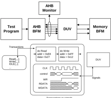
此階段的驗證,著重在 IP 硬體整體及其次模組(sub-module)的完整驗證,驗證 是否符合預期的結果與時序,預期的結果可與上一階段所得結果作比對,時序則 是次模組彼此整合在一齊時,是否符合制訂的介面。此外,在 IP 功能驗證上, 我們列出了所有必須驗證的功能項目(directed verification),也藉助了演算 法階段產生的 constrained random stimulus 來驗證 corner cases。在 AMBA AHB 介面上的功能驗證,使用 Synopsys bus functional model(BFM) 搭 配 monitor 來 驗 證 , 其 驗 證 環 境 如 圖 5 。 這 個 階 段 的 驗 證 是 採 transaction-based,也 就是把傳統驗證時直 接面對 signal 層次 ,提升到
transaction 的層次。這樣的作法可以讓驗證人員更專注於 IP 功能上驗證,而 不必直接面對訊號,再由驗證人員在訊號與功能裡做思考上的轉換。 AHB BFM DUV Memory BFM Test Program AHB Monitor Read(,,,); Write(,,,); IDLE(,,); ... DUV Transactions Signals do Read addr = 0xE8 data= 0x27 do Write addr = 0xFF data = 0x12 CLK control WR RDATA WDATA Transactions to signals 圖 5. Transaction-based AMBA 相容性驗證方法學
2.4 次系統整合(Sub-system integration)的驗證
我們將 DXB 整合到一個基本的 ARM-based SoC: ARM922T Example ARM SYstem (EASY),不過我們將原本 ARM 附的 Design Sign-off Model(DSM)以 Mentor Seamless 的 ARM922T XRAY ISS 取代,這樣做的目的是因為 ARM DSM 不容易作軟 體部份的 debugging,而 Seamless 的 tool 則提供了 source level 與 diassembly level 的 debugging 能力,此外,Seamless 也對系統模擬作了一些最佳化設計, 可加快系統的模擬,又不其準確性。
2.5 FPGA verification
我們利用 ARM Integrator 這套 rapid prototyping 系統來驗證 DXB,使用這套 系統的最大好處是系統上的諸多基本功能模組,如 timer、interrupt controller 等,與上個階段的環境一致,容易作驗證結果的比對,而在這一階段發現的問題, 可回到上一階段 debug,可補一般 FPGA 驗證不易 debug 的缺點。
2.6 Test plan/methods and testability measurement
Functional Coverage
我們將 DXB 內各子模組的功能經過仔細討論後,列出需要驗證的項目, 並逐一完成驗證,所以在我們所列的功能下 coverage 是 100%。 在 AMBA 介面,使用 Synopsys bus functional model(BFM)與 monitor
來檢驗。在支援的功能下,coverage 必須達到 100%。
Code Coverage
使用 TransEDA VN-Cover 產生的 coverage、必須符合下列條件:
Measurement Coverage(%) Statement 100 Branch 100 Path >50 Triggering 100 Toggle 100
使用 Debussy nLint 或 TransEDA VN-Check,檢查 coding style 是否 符合 XXX
Fault Coverage
test pattern,此 test pattern 的 fault coverage 至少為 95%以上。 測試考量與為測試所做的設計 由於 DXB 單晶片包含了多個複雜的次模組,如 DSP、FFT/IFFT、DAB/DVB accelerator IP 等等,測試晶片時要知道內部的訊號就會十分困難。因此 我們為測試所做的設計(Design-For-Testability, DFT)的解決方法就是針 對每個模組再包一層測試模組(test module),這個測試模組主要是由若干 個多工器及一些暫存器所組成,可以操作在正常模式和測試模式。當操作在 正常模式,要輸入的資料會透過測試模組直接送給次系統的輸入埠,其輸出 埠也是直接連接到其他相鄰次系統的輸入埠;操作在測試模式下時,被測試 的次系統輸入埠會改用測試的資料,而次系統測試輸出的結果會被存放在暫 存結果的暫存器內。 Module Under Test (MUT) 0 1 Normal Input Test Mode Input Normal output Test Mode Output TEST MODE Test Module 圖 7 測試模組和被測試模組的關係示意圖
3. 各子計畫摘要報告
本總計畫包括下列五個子計畫:
子計畫一: 以 OFDM 為基礎之 DAB 與 DVB-T 系統整合型接收機架構設計
A Unified Receiver Architecture Design for OFDM-based DAB and DVB-T Systems
計畫主持人:黃家齊教授
計畫編號:NSC 91-2218-E-009-009
子計畫二: 以正交分頻多工為基礎之多模式基頻收發器研製
The Study if an OFDM-Based Multimode Baseband Processor for Wireless Communications
計畫主持人:李鎮宜教授
計畫編號:NSC 91-2218-E-009-010 子計畫三: 數位訊號處理器與可重置加速器之設計
The Design of DSP Processor Core and Configurable Accelerator 計畫主持人:任建葳教授
計畫編號:NSC 91-2218-E-009-011
子計畫四:OFDM FFT 架構下軟體無線電訊處理之軟、硬體輔成設計及其數位通 信之應用設計
Efficient FFT-Based Software and Hardware Co-Design for OFDM-based SDR and its Application to Digital Communication 計畫主持人:陳紹基教授
計畫編號:NSC 91-2218-E-009-012
子計畫五: 針對無線通訊上佈局驅動的資料路徑合成器之研究
The Study on Layout-Driven Datapath Synthesis for Wireless Communication
計畫主持人:周景揚教授
計畫編號:NSC 91-2218-E-009-013
3.1 子計畫一:以 OFDM 為基礎之 DAB 與 DVB-T 系統整合型接收
機架構設計
中文摘要:本計畫將以三年的時間完成一個整合數位音響廣播和數位影像廣播地 面廣播系統基頻接收機架構的設計,以做為軟體定義無線電設計的參考。今年是 第一年,主要的工作是完成整合這兩個系統的訊號同步子系統接收機。在數位音 響廣播系統中,訊號同步子系統接收機將依次完成碼框同步、符元同步、小數載 波頻率偏移偵測以及整數載波頻率偏移偵測。而在數位影像廣播地面廣播系統 中,訊號同步子系統接收機則將依次完成符元同步、小數載波頻率偏移偵測、整 數載波頻率偏移偵測以及碼框同步。這兩個系統的訊號同步子系統接收機運作的 順序雖然不同,但是其架構相似,可以使用軟體控制的方法把這兩個訊號同步子 系統接收機整合起來。在這篇報告中,我們將提出一個整合這兩個訊號同步子系 統接收機的架構。然後以數位音響廣播系統的訊號同步子系統接收機架構為例, 用電腦模擬的方式測試這些訊號同步方法的效能。 關鍵詞:數位音響廣播,數位影像廣播地面廣播,基頻接收機架構,軟體定義無 線電,訊號同步子系統接收機,碼框同步,符元同步,小數載波頻率偏 移偵測,整數載波頻率偏移偵測。Abstract: This three-year project will be focused on designing an integrated receiver architecture in baseband for the DAB and the DVB-T broadcasting system. This integrated receiver architecture will be provided as a reference for the design of the SDR (Software Defined Radio). This is the first year and our major job is to completely integrate the receiver architectures of the signal synchronization subsystems for the two broadcasting systems. The receiver of the DAB signal synchronization subsystem will perform the frame synchronization, the symbol synchronization, the fractional frequency offset detection and the integral frequency offset detection sequentially. However, in the DVB-T system, the symbol synchronization, the fractional frequency offset detection, the integral frequency offset detection and the frame synchronization will be performed sequentially by the receiver of the signal synchronization subsystem. Although the receivers of these two subsystems do not perform in the same orders, their architectures are similar. We can use the software control method to integrate the receiver architectures of the two signal synchronization subsystems. In this report, we will propose an integrated receiver architecture for the two subsystems. Then, we will simulate these signal
synchronization methods based on the receiver architecture of the DAB signal synchronization subsystem, and discuss the performance of these methods.
Key Word: DAB, DVB-T, SDR (Software Defined Radio), signal synchronization
subsystem, frame synchronization, symbol synchronization, fractional frequency offset detection, integral frequency offset detection.
3.2 子計劃二:以正交分頻多工為基礎之多模式基頻收發器研製
中文摘要:此期中報告,主要針對數位視訊廣播系統(DVB-T)的正交分頻多工基頻 系統,進行關鍵技術的研究,包含同步子系統的演算法,高點數 FFT 處理器的設計, 和 FEC 中的 Viterbi 解碼器設計.為有效提供同步演算法的系統效能分析,系統 模擬平台的建立頗為重要,因此報告中包含三部份,分別為 DVB-T 系統模擬平台 的建構和開發,高點數 FFT 處理器的設計,和 Viterbi 解碼器設計.另外也包含出 國開會的會議論文和相關報告. 關鍵字: 數位視訊系統 正交分頻多工 同步演算法 FFT 處理器 Viterbi 解碼器 系統模擬平台Abstract: This report describes the project progress in developing core technologies for OFDM-based digital video broadcasting (DVB) system. The research tasks include the following: synchronization algorithm, high-point FFT processor design, and Viterbi decoder used in FEC processor. To provide a better environment for performance analysis of synchronization algorithms, a system simulation and design platform should be constructed first. And then all the rest key modules can be designed and simulated. There are 3 parts in this report, including DVB-T simulation platform, high-point FFT processor, and Viterbi decoder design. In addition, a technical report for attending an international conference (ESSIRCC2002) is appended for reference.
Keywords: DVB System, OFDM, Synchronization Algorithm, FFT processor,
3.3 子計畫三:數位訊號處理器與可重製加速器之設計
中文摘要:我們的計畫目標為設計一個應用在無線通訊的可程式化數位訊號處理 器(programmable DSP, or DSP processor),它擁有以下特性:(1) 高效能 (>2,000MOPS)、(2)高程式密度(good code density)、(3) 低功率(<1mW/MOP) 及(4) 可重新組態。超長指令字元(VLIW)處理器使用靜態排程而擁有可精準預估 的程式執行行為,故非常適用於高效能即時數位訊號處理的應用中。我們在本計 畫之第一年提出了一個嶄新的數位訊號處理器架構,它擁有單指令多資料(SIMD) 及可變長度之 VLIW 能力。我們同時也完成了指令集模擬器並評估了此處理器的 效能。此處理器解決了 VLIW 架構上兩個主要的問題:「指數成長的暫存器組」及 「極差的程式密度」。指令模擬結果顯示我們所提出的新架構擁有目前與市面上 高階數位訊號處理器可比擬的運算效能,但我們所使用的環狀暫存器組僅需要一 般架構不到一成(8.12%)的面積,速度卻是其 4.4 倍。另外,我們所提出的階層 式超長指令字元編碼更可省去 32%~50%的指令空間。 關鍵詞:數位訊號處理器、矽智產、暫存器組、可變長度之超長指令字元
Abstract: This project is to develop a programmable digital signal processor (programmable DSP or DSP processor) for wireless communications, which features: (1) high performance (> 2,000MOPS), (2) good code density, (3) low power (<1mW/MOP), and (4) configurability. VLIW processors with static instruction scheduling and thus deterministic execution times are very suitable for high-performance real-time DSP applications. In the first year of this project, we propose a novel variable-length VLIW DSP with SIMD capability and constructed its instruction set simulator (ISS) and evaluated the performance. The two major weaknesses in VLIW processors have been improved, which prevent the integration of more functional units (FU) for a higher instruction issuing rate – the exponentially growing complexity in the register file (RF), and the poor code density due to the NOP instructions. First, our proposed novel ring-structure RF partitions the centralized RF into 2N sub-blocks with an explicit N-by-N switch network for N FU. Each sub-block only requires access ports for a single FU. Second, we propose the hierarchical VLIW encoding with variable-length RISC-like instructions and NOP removal. The simulations show that our proposed instruction set architecture with the exposed ring-structure RF has comparable performance with state-of-the-art high-performance DSP processors. The ring-structure RF saves 91.88% silicon area and reduces 77.35% access time of the centralized RF. Moreover, the hierarchical VLIW encoding saves 32%~50% code sizes.
Keywords: digital signal processor (DSP), silicon IP, register file, variable-length
3.4 子計畫四:OFDM FFT 架構下軟體無線電訊號處理之軟、硬體
輔成設計及其數位通信之應用設計
中文摘要:在這個計劃中已經得到了五個進展成果。第一個部分是關於可變長度 的快速傅利葉轉換處理器所使用的資料位址產生器設計;另一方面,對於傅利葉 轉換中所需要的旋轉因數指標產生器亦是可變長度快速傅利葉轉換處理器中的 重要設計,在這裡共有二個用於固定基數演算法與一個用於分裂基數演算法的旋 轉因數指標產生器設計將會在第二部分提出。為了減少儲存旋轉因數所佔用的硬 體成本,第三部份會介紹一個以遞迴方程式來產生正弦與餘弦函數的旋轉因數產 生器設計。第四部份是一個範例性質的可變長度快速傅利葉轉換處理器整合實 作。最後一部份是一個結合 DCT 技術設計出之一新的高效能之 OFDM 通道估測演 算法。 關鍵字:快速傅利葉轉換、位址產生器、係數產生器、正交分頻多工、數位聲訊 廣播、數位視訊廣播。Abstract: There are five intermediate results generated so far from our on-going project. The first four results are related to the IFFT processor design for the demodulation of OFDM-based wireless/wireline communication systems including DAB, DVB, 802.11a, 802.16 and VDSL systems. The four IFFT related results are: (1) a data address generator designed for memory-based, variable-length FFT processor; (2) three new architectures for coefficient index generation, which can work efficiently with the mentioned variable-length data address generator, where the first two are for fixed-radix FFT algorithm and the third one is for split-radix 2/4 FFT algorithm; (3) a new coefficient generator which can replace conventional high-cost coefficient ROM; (4) a variable-length FFT processor which integrates the advance technologies is proposed in part 4. Finally, we also developed a high-performance channel estimation algorithm based on DCT.
3.5 子計畫五:針對無線通訊上佈局驅動的資料路徑合成器之研究
中文摘要:由於半導體技術的突飛猛進,單晶片系統(SoC)已經變成了二十一世 紀裡的主流科技,藉由單晶片系統的技術,可以加速促成三 C(電腦、通訊、民 生家電)之間的整合,這不管對企業或是科技來說,都是一股不可避免的潮流, 對整個人類社會來說,三 C 的整合應用更是一個非常重要的進步。 以往人們的期望只是一個快速、可靠且容易使用的無線通訊系統,但現在人 們的要求已不僅僅如此,他們期待能有更快速的方法來透過無線通訊存取資料, 以便應付現在的各種應用,例如收發電子郵件、檔案傳輸協定、網路瀏覽器、甚 至即時影像傳輸等等,對無線服務提供的廠商來說,它們若想繼續保有競爭力, 就必須跟上這個時代潮流。在這個整合計畫中,我們主要就是針對 Beyond 3G(B3G) 的無線通訊網路來做研究,特別是其中的單晶片系統技術。 在 B3G 的無線通訊系統中,如何設計一個速度又快、面積又小的乘法器是非 常重要的,因為乘法器是系統中許多重要部分如中央處理器(CPU)、數位訊號處 理器(DSP)、快速傅立業轉換器(FFT)裡的關鍵元件。 在前一年的研究中,我們提出了一個以佈局導向為考量的自動乘法產生器。 對於時序的計算,我們採用了以單位元件為基礎的延遲模型(cell-based delay model),而非傳統電路設計中被廣為使用的互斥邏輯閘的延遲模型(XOR-based delay model);同時,在電路合成的過程中,加入了繞線延遲(wire delay)的效 應,使得時序的計算將能更貼近實際電路的情形。除此之外,在電路配置 (placement)的過程當中,不僅對於時序做了最佳化,還同時考慮了電路的形狀, 使其能趨近於方正。藉由將電路合成、配置以及再合成等步驟整合在乘法產生器 的流程,我們將可以得到優於其它傳統作法所產生的乘法器。 在此次計畫中,我們提出了由誤差大小來決定硬體的自動乘法產生器。藉著 容許些許的誤差,我們可以用更小的面積來實現更快速的乘法器。考慮到信號到 達時間的曲線圖,我們也為以時間為考量的繞線和電路配置(placement) 提出一 些技巧,來做時序最佳化。在乘法產生器的流程中,藉由整合電路合成、配置以 及再合成的步驟,我們將可得到優於其他傳統作法產生的乘法器。Abstract: With the advent of semiconductor technology, the System-on-a-chip (SoC) becomes a mainstream and focus of technologies on coming 21st century. The integration of Computing, Communication and Consumer Electronics will be speeded up through SoC, which causes the unavoidable trend of new era for technology and enterprises. Especially, the application of 3C integration is very important to the progress of human being society.
People all over the world have come to expect fast, reliable, and easily accessible wireless communications and now they are demanding faster ways to access data with applications as diverse as e-mail, file transfer protocol, Internet browsers, and even real-time video teleconferencing. Wireless service providers who want to remain competitive must keep pace with this demand. In this integrated project, we are targeting on the study of beyond 3G wireless networks. Particularly, we are focusing on SoC technologies for OFDM-based SDR baseband processing.
To design fast, area-efficient and low power multipliers is important because multiplication is a key operation in many processors such as CPU, DSP and
FFT/IFFT processors for the wireless communications.
In previous research, we presented an automatic layout-driven multiplier generator. The cell-based delay model, rather than the XOR-based model, is used for timing estimation and the wire delay is also considered in the synthesis process. The timing optimization, by considering the shape of the circuit, is conducted in the placement process. Final adder is produced together with the column compression tree for getting the simpler structure. By integrating synthesis, placement and resynthesis processes in the multiplier generation flow, the multipliers generated by our layout-driven multiplier generator outperform other previous works as shown in our experimental results.
In this project, we present an automatic error-controlled hardware-configurable multiplier generator. The determination of the hardware of a multiplier is based on the error constraint given by users. With allowing some rounding errors, a significant reduction in area and delay can be achieved. By considering signal arrival profile, we also proposed several techniques for timing driven routing and placement to optimize the timing. By integrating synthesis, placement and resynthesis processes in the multiplier generation flow, the multipliers generated by our multiplier generator outperform other schemes used for comparison as shown in our experimental results.