國立交通大學
光電工程學系博士班
博 士 論 文
新穎矽量子點薄膜應用於太陽能電池之開發
Development of Novel Si Quantum Dot Thin Films
for Solar Cells Application
博士生:郭光揚
指導教授:李柏璁 教授
新穎矽量子點薄膜應用於太陽能電池之開發
Development of Novel Si Quantum Dot Thin Films
for Solar Cells Application
研 究 生:郭光揚 Student:Kuang-Yang Kuo
指導教授:李柏璁 Advisor:Po-Tsung Lee
國 立 交 通 大 學
光電工程學系博士班
博 士 論 文
A ThesisSubmitted toDepartment of Photonics,
College of Electrical Engineering and Computer Science National Chiao Tung University
in partial Fulfillment of the Requirements for the Degree of Doctor of Philosophy
in
Electro-Optical Engineering Aug. 2013
Hsinchu, Taiwan, Republic of China
中華民國一百零二年八月
I
新穎矽量子點薄膜應用於太陽能電池之開發
學生:郭光揚
指導教授:李柏璁 博士
國立交通大學光電工程學系博士班
摘 要
『溫室效應』與『能源危機』乃攸關未來人類生存的兩大重要議題,永續再 生能源加速發展已刻不容緩,而太陽能電池(Solar Cell, SC)一直被視為極具潛力 的再生能源之一。於考量電池效率、成本和壽命等關鍵因素下,矽基 SC 仍是最 具有優勢可達到普及化的電池種類;為了達到高效率低成本(第三代 SC)矽基 SC, 開發具有多重能隙的多接面元件結構以有效減低光損耗是不可或缺的要件。 有鑒於矽量子點的獨特光學特性,我們提出並開發『漸變矽過多氧化矽多層 膜』與『氧化鋅矩陣材料整合』,期望能在保有矽量子點特性下,同時克服目前 應用於 SC 所遭遇的載子傳輸效益明顯受限的瓶頸,以製作出更具應用潛力的新 穎矽量子點薄膜。此篇論文首先即介紹 SC 的重要性和發展現況,與目前矽量子 點應用於 SC 的優勢與挑戰,並提出我們的研究目的且簡介此研究過程中的相關 製程與分析儀器。 為製作出超高密度矽量子點薄膜,我們捨棄傳統的[二氧化矽/矽過多氧化矽] 多層膜結構,改以『漸變矽過多氧化矽多層膜』做為新沉積結構;實驗結果顯示, 藉由週期性矽氧原子濃度差異分佈,可使矽過多原子於退火過程中自組織形成超 高密度且均勻尺寸的奈米結晶矽量子點,此外,該新結構亦大幅提升矽量子點薄 膜的光吸收係數與電傳輸效益,證明利用此新結構,可有效縮短矽量子點間距, 以大幅提升矽量子點薄膜的光伏特性。 為形成更佳的載子傳輸機制,我們亦開發『氧化鋅矩陣材料整合』,因氧化 鋅薄膜除具備直接寬能隙半導體特性之外,更罕見地同時擁有高透明度和高可調 電性等優勢,故相當適合做為矽量子點矩陣材料並應用於 SC;實驗結果指出,II 針對該矽量子點埋入式氧化鋅薄膜,除在長與短波長波段皆可分別保有氧化鋅的 高光穿透與高光吸收特性之外,中波長波段亦具有來自矽量子點的光吸收與光激 發光特性,證實來自矽量子點貢獻的光學次能隙形成;此外,相較於使用傳統矽 相關介電矩陣材料,該矽量子點薄膜具有更高的導電度,且其載子主要經由氧化 鋅矩陣傳輸而非傳統的量子點間穿隧效應傳輸,此經矩陣傳輸機制將可大幅提升 矽量子點薄膜的載子傳輸效益,未來亦可更提升矽量子點應用於 SC 的優勢。 因此,此篇論文中,藉由分別開發新沉積結構與新矩陣材料,我們成功製作 出更具潛力且更適合整合於矽基 SC 的新穎矽量子點薄膜,而根據此研究成果, 我們更深信未來若能成功整合此新穎矽量子點薄膜,將可有利於矽基 SC 的發展, 並加速邁向第三代 SC 的目標。
III
Development of Novel Si Quantum Dot Thin Films
for Solar Cells Application
Student: Kuang-Yang Kuo
Advisor:Dr. Po-Tsung Lee
Department of Photonics
National Chiao Tung University
Abstract
In order to resolve the critical issues of “Green House Effect” and “Energy
Crisis” for humanity’s future, the accelerated developments of renewable energies are
necessary. Among all of the renewable energies, solar cells (SCs) are highly considered as the most potential one. To ponder these key factors of efficiency, cost, and lifetime, undoubtedly, the Si-based SCs have the most advantages on popularized developments in the future. However, to successfully achieve high efficiency and low cost, also called the third generation SC, the tandem Si-based SCs with multi-bandgap is required to efficiently reduce the mismatched photon energy loss.
Based on the unique properties of Si quantum dot (QD), we propose to develop the novel Si QD thin films by utilizing a gradient Si-rich oxide multilayer
(GSRO-ML) structure and integrating with ZnO matrix material to overcome the
bottlenecks of the largely limited carrier transport efficiency in the Si-based SCs integrating Si QDs. In the beginning of this dissertation, we talk about the importance and recent developments of SCs, and then, the advantages and challenges of SCs integrating Si QDs are discussed. After that, our motivations, fabrication process, and apparatus are also introduced in details.
To achieve the formation of super-high density Si QD thin films, we forsake the traditional [SiO2/SRO]-ML structure and develop a new one, GSRO-ML. In our
IV
deposition, the Si QDs with super-high density and good size control can be self-assembled from the uniform aggregations of Si-rich atoms during annealing. Besides, the considerable enhancements on photovoltaic properties are also obtained by using a GSRO-ML structure due to the improved carrier transport efficiency and larger optical absorption coefficient.
To obtain the better carrier transport path for the Si QD thin films, we also develop a new matrix material, ZnO, because it has many desirable features, such as
wide and direct bandgap, high transparency, and highly tunable electrical properties. In our results, though embedded with Si QDs, the optical properties of
ZnO thin film can be preserved in the long- and short-wavelength ranges. In the middle-wavelength range, the significantly enhanced light absorption and the unusual PL emission peak, owing to embedding Si QDs, are observed. These results represent the sub-bandgap formation in ZnO thin film by utilizing Si QDs while maintaining the essential optical properties of ZnO matrix. In the electrical properties, the Si QD embedded ZnO thin film reveals the significantly higher conductivity than that using SiO2 matrix material. Besides, the carriers transport mainly via ZnO matrix, not
through Si QDs, is clearly observed. This unique transport mechanism differing from those using the traditional Si-based dielectric matrix materials has great potential on leading to the much better carrier transport efficiency and electrical properties for SC applications.
In this dissertation, we had demonstrated the proposed novel Si QD thin films,
utilizing a GSRO-ML structure and integrating with ZnO matrix material, are
more suitable and advantageous for the Si-based SCs integrating Si QDs. Therefore, the high-efficiency Si-based SCs integrating Si QDs can be most definitely expected using the novel Si QD thin films.
V
Acknowledgements
首先,要特別感謝我的指導教授-李柏璁 教授,這些年在實驗和研究上給我 許多寶貴建議與發揮空間,以及在報告技巧、期刊寫作與思考邏輯各方面的諸多 指導,經過這幾年的歷練後,能力著實增進不少,非常感謝李教授這些年不辭辛 勞的教誨,也很慶幸自己能來到交大,來到李教授的實驗室。 在實驗執行上,感謝這幾年合作過的學弟妹們-書維、文齡、品睿、權政與佑 政,因為有你們的盡心盡力,不僅讓實驗與計畫皆得以順利執行,也幫我分攤不 少儀器管理上的負擔;感謝學長們-Dr.盧贊文與 Dr.張資岳在我博班期間提供許多 建議與協助,以及浪人品佐於部份實驗上的支援,公務員家揚的定期刺激,拼命 三郎佳裕於儀器管理上的協助;也感謝已經畢業的學弟妹們-逸華、欣育、怡先、 韋德、宜恆、又瑋、鈞隆、君源、立勛、雋崴、哲堯與小朱哥等,以及實驗室充 滿朝氣的生力軍-坤達、家瑞、擇恩與聖諺以及新生們,讓我在交大博士班充滿 許多難忘回憶,也替我的學生生涯畫下一個非常漂亮的句點。 在研究經費上,要感謝國科會-能源國家型整合計畫(計畫編號: NSC 98-3114- E-009-004-CC2 與 NSC 99-2120-M-009-009),以及國立交通大學的綠色能源中心 與特色計畫所提供的計畫經費,讓我的博班研究工作能順利進行。 最後,我更要特別感謝我的家人,諒解我這些年來的執著,讓我在整個求學 的漫漫長路上沒有過多的經濟壓力,且總是適時的關心,你們依舊是我最堅強的 後盾!另外,我的好朋友們-威浤、信智、宗諭、翊翔、宇倫、廣騰、應文、文 賢與若軒等等,感謝你們總是在我最需要幫助的時候,二話不說的伸出雙手雙腳, 情義相挺,真的是太夠朋友了! 在此,對於這一路上曾經幫助過我的貴人們,獻上最誠摯的謝意,沒有你們, 沒有今天的我! 郭光揚 2013/09/09VI
Table of Contents
Abstract (in Chinese) ……….I Abstract (in English) ………III Acknowledgements ……….V Table of Contents ………VI Figure Captions ………...IX Table Captions ………XVII
Chapter 1 Introduction of Si Quantum Dot (QD) Thin Films for Solar Cells
Application 1
1-1 Background of Solar Cells ………..1
1-2 Solar Cells Integrating Si QD Thin Films ………4
1-2.1 Energy Loss Mechanisms ………4
1-2.2 Advantages of Using Si QD ……….6
1-2.3 Literatures Review ………...7
1-3 Applications on Other Optoelectronic Devices ……….11
1-4 Motivation for Solar Cells Application ……….12
1-4.1 Si QD Thin Films Utilizing a Gradient Si-rich Oxide Multilayer (GSRO-ML) Structure ……….13
1-4.2 Si QD Thin Films Utilizing ZnO Matrix Material ……….14
1-5 Summary ………...16
Chapter 2 Experimental Apparatus 17
2-1 Apparatus for Sample Fabrication ………17
2-1.1 Wet-Bench and Ultrasonic Cleaner ……….17
2-1.2 Radio-Frequency Magnetron Co-Sputtering System ………18
2-1.3 Furnace Annealing System ………20
VII
2-1.5 Thermal Evaporator ………...23
2-2 Apparatus for Characterization Measurement ………...24
2-2.1 Micro-Raman Spectroscopy ………..24
2-2.2 Micro-Photoluminescence Spectroscopy ………..25
2-2.3 X-Ray Diffractometer ………26
2-2.4 Ultraviolet/Visible/Near-Infrared Spectroscopy ………27
2-2.5 Atomic Force Microscope ……….28
2-2.6 Transmission Electron Microscope ………...29
2-2.7 Semiconductor Device Measurement System ………...31
2-2.8 Solar Simulator Measurement System ………..32
2-2.9 Quantum Efficiency Measurement System ………...33
Chapter 3 Si QD Thin Films Utilizing a Gradient Si-rich Oxide Multilayer (GSRO-ML) Structure 34
3-1 Sample Fabrication ………...34
3-2 Nano-Crystalline and Structural Properties ………...36
3-3 Photoluminescence Emission and Optical Absorption Properties …………39
3-4 Photovoltaic Properties and Carrier Transport Mechanism ………..42
3-5 Summary ………...45
Chapter 4 Si QD Thin Films Utilizing ZnO Matrix Material 47
4-1 [ZnO/Si] ML Thin Films Annealed by Rapid Thermal Annealing ………...47
4-1.1 Sample Fabrication ………47
4-1.2 Nano-Crystalline Properties ……….47
4-1.3 Formation Mechanism ………..49
4-1.4 Summary of Section 4-1 ………...52 4-2 [ZnO/Si] ML Thin Films Annealed under a Shorter Duration by Furnace
VIII
Annealing ………53
4-2.1 Sample Fabrication ……….53
4-2.2 Nano-Crystalline Properties ……….53
4-2.3 Optical Properties and Sub-Bandgap Formation ……….56
4-2.4 Summary of Section 4-2 ………59
4-3 [ZnO/Si] ML Thin Films Annealed under a Longer Duration by Furnace Annealing ………60
4-3.1 Sample Fabrication ………60
4-3.2 Nano-Crystalline Properties ………60
4-3.3 Optical Transmittance Improvement ……….62
4-3.4 Local Film Prominences ………63
4-3.5 Electrical Properties and Carrier Transport Mechanism ………64
4-3.6 Summary of Section 4-3 ………67
4-4 Summary ………...69
Chapter 5 Conclusion and Future Works 70
5-1 Conclusion ………..70
5-2 Future Works ………72
5-2.1 All Si QD Thin Film Solar Cells Utilizing a GSRO-ML Structure …...72
5-2.2 Si QD Embedded ZnO p-n Homojunction Devices ……….73
Appendix: Developments of Heavily B- and P-doped Si QD Thin Films 74
A-1 Heavily B-doped Si QD Thin Films ……….74
A-2 Heavily P-doped Si QD Thin Films ……….77
A-3 Summary ………..78
References 79
IX
Figure Captions
Chapter 1
Fig. 1-1: Prediction for the development of the global energy mix (~2100). [1] ...2 Fig. 1-2: (a) Prediction of the market shares 2015 for the main kinds of SCs. [2] (b) Composition of the main elements in the earth’s crust. [3] ………2 Fig. 1-3: Best research-cell efficiencies recorded by NREL (~2013). [5] ……..3 Fig. 1-4: Efficiency versus cost for three generations of SCs. [5] ………4 Fig. 1-5: Main energy loss mechanisms in SCs with single bandgap, including the (1) over-high photon energy loss, (2) junction loss, (3) recombination loss, (4) metal-semiconductor contact loss, and (5) over-low photon energy loss. ……….5 Fig. 1-6: Difference of photon absorption between SCs with (a) single- and (b)multi-bandgap. ………..5 Fig. 1-7: Solar irradiance spectrum above atmosphere and at surface. [6] ……..5 Fig. 1-8: Illustration of band diagrams for Si QDs embedded in a wide bandgap matrix material under different QD sizes. ………..6 Fig. 1-9: Illustration of a possible design for an all Si-based tandem SC integrating Si QDs with different QD sizes. ……….7 Fig. 1-10: Illustration of the fabrication process for the Si QD thin films using a [SiO2/SRO]-ML structure. [13] ……….8
X
Fig. 1-11: (a) Low and (b) high magnification TEM images of the Si QD thin films using a Si3N4 matrix material. [13] ………8
Fig. 1-12: Bandgap energy versus QD size using SiO2 and Si3N4 matrix materials
from different groups’ works. [13] ………9 Fig. 1-13: Illustration of a n-type Si QDs/p-type c-Si SC. [16] ………10 Fig. 1-14: Internal quantum efficiency (IQE) and corresponding absorption spectra of the fabricated n-type Si QDs/p-type c-Si SCs. [16] ………..10 Fig. 1-15: Illustration of the Si QD thin film fabricated by using a [SiO2/SRO]-ML
deposition structure. ……….12 Fig. 1-16: Illustrations of the main carrier transport process in the Si QD thin films fabricated by using the (a) traditional [SiO2/SRO]-ML and (b) novel
deposition structures. The thicker lines in (b) than that in (a) represent the larger tunneling probability obtained. ………..14 Fig. 1-17: Illustration of the Si QD thin film fabricated by using our proposed GSRO-ML deposition structure. ………14 Fig. 1-18: Illustrations of the main carrier transport process for Si QDs embedded in an (a) insulated or (b) semi-conductive matrix material. The lines with different color represent the different carrier transport mechanism. ….15
Chapter 2
Fig. 2-1: Images of the (a) wet-bench and (b) ultrasonic cleaner. ………17 Fig. 2-2: (a) Outside and (b) inside images of the RF magnetron co-sputtering system. ………...19
XI
Fig. 2-3: Illustration of a sputtering deposition process. ……….19 Fig. 2-4: Images of the furnace annealing system and its main components. …..20 Fig. 2-5: Illustration of a furnace annealing process. ………21 Fig. 2-6: Image of the reactive ion etching system (RIE200L, SAMCO). ……22 Fig. 2-7: Illustration of a reactive ion etching process. ((1) and (4): two electrodes, (2): F- ions, (3): electric field, (5): samples) [4] ………22 Fig. 2-8: Image of the thermal evaporator. ………..23 Fig. 2-9: Illustration of a thermal evaporation process. [5] ……….23 Fig. 2-10: Image of the micro-Raman and micro-photoluminescence (PL) spectro- scopy (Horiba LabRam HR). ……….24 Fig. 2-11: Illustration of a micro-Raman spectroscopy system and its measurement process. [6] ………24 Fig. 2-12: Illustration of a micro-PL spectroscopy system. [7] ……….25 Fig. 2-13: Image of the X-ray diffractometer (Bede D1). ……….26 Fig. 2-14: Illustration of the grazing incident X-ray diffraction method. [8] ……26 Fig. 2-15: Image of the ultraviolet/visible/near-infrared spectroscopy (Hitachi U- 4100). ………27 Fig. 2-16: Illustration of an ultraviolet/visible/near-infrared spectroscopy. [9] …27 Fig. 2-17: Image of the atomic force microscope (D3100). ………..28
XII
Fig. 2-18: Illustration of an atomic force microscope using a beam deflection detection method. [10] ………..28 Fig. 2-19: Image of the transmission electron microscope (JEOL JEM-2010F). …29 Fig. 2-20: Illustration of a transmission electron microscope. [11] ………...30 Fig. 2-21: Image of the precision ion polishing system (Gatan 691). ………30 Fig. 2-22: Image of the semiconductor device measurement system. …………...31 Fig. 2-23: Images of the main components of the semiconductor device measure- ment system: (a) measurement station, (b) Agilent E5270B precision measurement mainframe, and (c) halogen light source. ……31 Fig. 2-24: Image of the solar simulator measurement system (Newport). ………32 Fig. 2-25: Illustration of the solar simulator measurement system. ………..32 Fig. 2-26: Image of the quantum efficiency measurement system (Hitachi QE- 3000). ………..33 Fig. 2-27: Illustration of a quantum efficiency measurement system. [12] ……..33
Chapter 3
Fig. 3-1: Fig. 3-1: Variations of the Si and SiO2 sputtering powers during
deposition for sample GSRO-ML. ……….35 Fig. 3-2: Illustrations of film structures for samples (a) GSRO-ML and (b) [SiO2/SRO]-ML before and after annealing. ………36
XIII
Fig. 3-4: High-resolution TEM images of samples (a) [SiO2/SRO]-ML and (b)
GSRO-ML. (c) The corresponding QD size distributions. ………38 Fig. 3-5: PL spectra and the fitting curves of samples GSRO-ML and [SiO2/SRO]-
ML. ……….40 Fig. 3-6: I-V curves of samples GSRO-ML and [SiO2/SRO]-ML with and without a
488 nm laser illumination. ………..41 Fig. 3-7: Absorption spectra of samples GSRO-ML and [SiO2/SRO]-ML. Inset
shows the corresponding Tauc plots for indirect allowed transition. ….42 Fig. 3-8: (a) Illustration of the device structure for I-V measurements and (b) the dark I-V curves of samples GSRO-ML and [SiO2/SRO]-ML. Inset shows
the corresponding light I-V curves under a halogen lamp illumination. ...43 Fig. 3-9: Dark forward I-V curves in log-log scale for samples (a) [SiO2/SRO]-ML
and (b) GSRO-ML. ………44 Fig. 3-10: Temperature-dependent dark I-V curves of samples (a) [SiO2/SRO]-ML
and (b) GSRO-ML. Inset of (b) shows the parameter B in region II. ………45
Chapter 4
Fig. 4-1: (a) Raman spectra and (b) XRD patterns of the annealed [ZnO/Si] ML thin films under different PSi. Inset of (a) shows the curve-fitting result of
Raman spectrum for sample S110. ………..48 Fig. 4-2: AFM images of (a) the ZnO single-layer with a 5 nm thickness and the [ZnO/Si] single-bilayer thin films under (b) 25, (c) 75, (d) 90, and (e) 110 W of PSi after deposition. ………50
XIV
Fig. 4-3: The overall and zoom-in cross-sectional TEM images of the [ZnO/Si] ML thin film. (a) and (b) are as-deposited, and (c) and (d) are after annealing for sample S110. ………...51 Fig. 4-4: Illustration of the formation of nc-Si QDs embedded in the crystalline ZnO matrix with a high enough PSi by using a [ZnO/Si] ML
structure. ………...…52 Fig. 4-5: (a) The curve-fitting result of Raman spectrum for sample FA-1000. (b) Raman spectra of the [ZnO/Si] ML thin films under different Tann. Inset
shows the XRD pattern for sample FA-1000. ………54 Fig. 4-6: Cross-sectional TEM images of the (a) as-deposited and (b) 1000°C- annealed (sample FA-1000) [ZnO/Si] ML thin films. Insets show the corresponding overall images. ………...56 Fig. 4-7: PL spectra of sample FA-1000 and pure ZnO thin film after annealing at 1000°C. ………..57
Fig. 4-8: (a) Transmission, reflection, and (b) absorption spectra of sample FA-1000 and pure ZnO thin film on quartzes. (c) PL spectrum and Tauc plot for indirect allowed transition of sample FA-1000. Inset shows the Tauc plot for direct allowed transition of sample FA-1000. …………59 Fig. 4-9: Raman spectra of the Si QD embedded ZnO thin films under different Tann.
Inset shows the corresponding crystalline volume fractions of Si (fc-Si). ……….61
Fig. 4-10: (a) XRD patterns fine-scanned from 30° to 40° of the Si QD embedded ZnO thin films under different Tann. (b) Full XRD pattern of the Si QD
embedded ZnO thin film annealed at 700°C. Inset of (b) shows the curve-fitting result for the main diffraction signal. ………..62
XV
Fig. 4-11: Optical transmittance spectra of the Si QD embedded ZnO thin films under different Tann. ……….63
Fig. 4-12: (a) Cross-sectional SEM image and (b) local film prominence density and diameter in average for the Si QD embedded ZnO thin films after annealing. ……….64 Fig. 4-13: (a) Resistivity of the Si QD embedded ZnO thin films under different Tann.
(b) Logarithmic I-V curve of sample annealed at 700°C, and inset shows the linear I-V curve in magnification. ………65 Fig. 4-14: (a) Forward I-V curves for different measurement temperatures, (b) the parameter B, and (c) Arrhenius plot of ln(Is) versus 1000/T for the Si QD
embedded ZnO thin film annealed at 700°C. ………67
Chapter 5
Fig. 5-1: Illustration of device structure and band diagram for the single- and multi-junction Si-based tandem SCs integrating Si QDs. ……….73
Appendix
Fig. A-1: (a) Hole concentration and mobility and (b) resistivity of the heavily B-doped Si QD thin films on n-type Si wafers under different B sputtering powers. ………..74 Fig. A-2: Solar simulator (AM 1.5G) illuminated I-V curves of the heavily B-doped
Si QD thin films on n-type Si wafers under different B sputtering powers. ………75 Fig. A-3: Parameters of (a) VOC and JSC and (b) F.F. and η of the heavily B-doped Si
QD thin films on n-type Si wafers under different B sputtering powers. ……….76
XVI
Fig. A-4: (a) Absorption coefficient spectra and (b) the corresponding optical bandgaps of the heavily B-doped Si QD thin films on n-type Si wafers under different nucleation layer thicknesses. ………76 Fig. A-5: (a) Full and (b) magnified internal quantum efficiency spectra of the
heavily B-doped Si QD thin films on n-type Si wafers under different nucleation layer thicknesses. ……….77
XVII
Table Captions
Chapter 3
Table 3-1: Curve-fitting results from Raman spectra for the crystalline properties of samples GSRO-ML and [SiO2/SRO]-ML. ……….37
Table 3-2: Curve-fitting results from PL spectra of samples GSRO-ML and [SiO2/SRO]-ML. ………40
Chapter 4
Table 4-1: Parameters of the curve-fitting results in Raman spectra for nc-Si phase and the calculated crystalline volume fractions of Si (fc-Si) under
1
Chapter 1
Introduction of Si Quantum Dot (QD) Thin Films for Solar
Cells Application
1-1
Background of Solar Cells
Recently, in order to resolve the critical issues of “Green House Effect” and “Energy Crisis” for humanity’s future, the demands on the non-renewable resources, for examples, coil, coal, and natural gas, are necessary to be largely reduced in the near-future. Hence, it’s very important to accelerate the developments on the renewable energies, such as solar cell (SC), solar thermal energy, biomass energy, wind power, and hydropower. Fig. 1-1 shows an illustration for the development of the global energy mix (~2100) predicted by German Solar Industry Association [1].It clearly indicates the energies created by SCs will be the most important source after 2050 because of the large area and long duration of solar irradiation on the earth. Therefore, the popularized development of SCs can efficiently improve the critical issues of “Green House Effect” and “Energy Crisis” in the future.
Fig. 1-2(a) shows the predicted market shares 2015 for the main kinds of SCs by EuPD Research [2], it clearly indicates the Si-based SCs, involving the c-Si bulk and Si thin film SCs, will still occupy the highest market share for 82 % in 2015. Besides, the content of Si element in the earth’s crust is the largest material among all kinds of SCs, shown as Fig. 1-2(b) [3]. Hence, the Si-based SCs have many advantageous on the popularized development in the future. The newly-updated best research-cell efficiencies (~2013) recorded by National Renewable Energy Laboratory (NREL) are also shown in Fig. 1-3 [4], so far, the conversion efficiencies of the Si-based SC are
2
still significantly limited by the energy loss mechanisms [5]. Therefore, to efficiently reduce the energy loss in the Si-based SCs is needed to further enhance the SCs’ performances.
Fig. 1-1: Prediction for the development of the global energy mix (~2100). [1]
Fig. 1-2: (a) Prediction of the market shares 2015 for the main kinds of SCs. [2] (b) Composition of the main elements in the earth’s crust.[3]
3
Fig. 1-3: Best research-cell efficiencies recorded by NREL (~2013). [5]
Based on efficiency and cost, the SCs can be briefly classified to three generations, shown as Fig. 1-4 [5]. The first generation SCs have the high efficiency but high cost, such as single- and poly-crystalline Si bulk SCs; and the second generation ones possess the low cost but low efficiency, such as organic and dye-sensitized (DSSC) SCs. And so far, the third generation SCs with high efficiency and low cost are still unsuccessfully developed, however, the tandem SCs with multi-bandgap are highly expected due to the great potentials on the mismatched photon energy loss improvements [5].
4
Fig. 1-4: Efficiency versus cost for three generations of SCs.[5]
1-2
Solar Cells Integrating Si QD Thin Films
1-2.1 Energy Loss Mechanisms
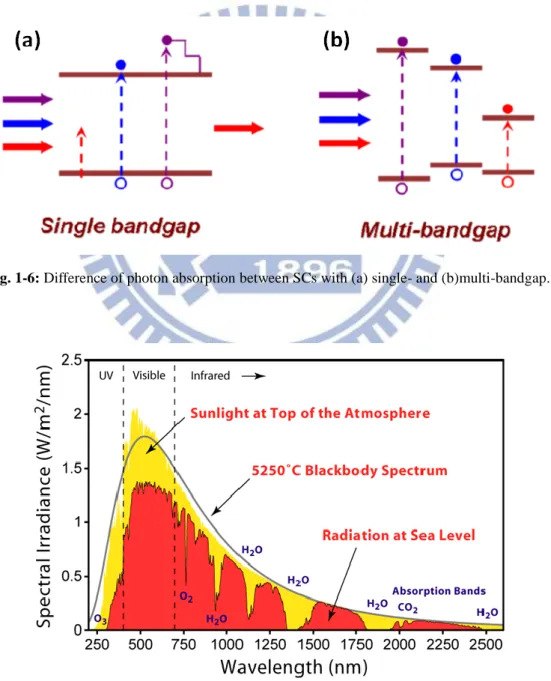
So far, the performances of SCs with single-bandgap are mainly limited by five kinds of energy loss mechanisms, including the over-high photon energy loss, junction loss, recombination loss, metal-semiconductor contact loss, and over-low photon energy loss [5], as shown in Fig. 1-5. The difference of photon absorption between SCs with single- and multi-bandgap is also shown in Fig. 1-6 [5]. Better than with single-bandgap, the SCs with multi-bandgap can efficiently improve the over-high and over-low photon energy losses and significantly enhance cells’ performances. As the solar irradiation energies are widely distributed in a large wavelength range, shown as Fig. 1-7 [6], the mismatched photon energy loss will largely degrade the performances of SCs with single-bandgap. Hence, the SCs with multi-bandgap are more potential for the third-generation SCs development than that with single-bandgap.
5
Fig. 1-5: Main energy loss mechanisms in SCs with single bandgap, including the (1) over-high photon
energy loss, (2) junction loss, (3) recombination loss, (4) metal-semiconductor contact loss, and (5) over-low photon energy loss.
Fig. 1-6:Difference of photon absorption between SCs with (a) single- and (b)multi-bandgap.
6 1-2.2 Advantages of Using Si QD
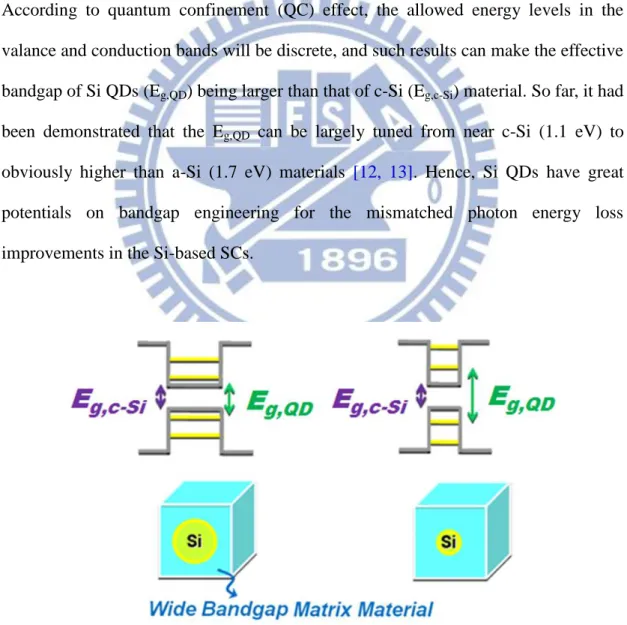
In order to efficiently reduce the mismatched photon energy loss in the Si-based SCs, the Si QD thin films have been extensively studied owing to their many unique characteristics such as highly-tunable bandgap and better optical properties [7-9]. The Si-based dielectric materials, such as SiO2 and Si3N4, are commonly used as the
matrix materials due to their simple process, high transparency, and significantly larger bandgap than c-Si material [10, 11]. Fig. 1-8 shows the band diagrams of Si QDs embedded in a wide bandgap matrix material under different QD sizes. According to quantum confinement (QC) effect, the allowed energy levels in the valance and conduction bands will be discrete, and such results can make the effective bandgap of Si QDs (Eg,QD) being larger than that of c-Si (Eg,c-Si) material. So far, it had
been demonstrated that the Eg,QD can be largely tuned from near c-Si (1.1 eV) to
obviously higher than a-Si (1.7 eV) materials [12, 13]. Hence, Si QDs have great potentials on bandgap engineering for the mismatched photon energy loss improvements in the Si-based SCs.
Fig. 1-8: Illustration of band diagrams for Si QDs embedded in a wide bandgap matrix material under
7
Fig. 1-9 shows an illustration of a possible design for an all Si-based tandem SC integrating Si QDs with different QD sizes. By integrating various QD sizes, the mismatched photon energy loss can be efficiently reduced, and the cell’s performance can also be significantly enhanced. Therefore, the third generation Si-based SCs with high efficiency and low cost can be highly expected by integrating Si QDs.
Fig. 1-9: Illustration of a possible design for an all Si-based tandem SC integrating Si QDs with
different QD sizes.
1-2.3 Literatures Review
In 2006, M. A. Green at al. firstly proposes the idea of integrating Si QDs with Si-based SCs for the third generation SCs [10, 14]. They fabricate the Si QD thin films by radio-frequency (RF) co-sputtering and post-annealing methods, shown as Fig. 1-10. The Si QD embedded SiO2 thin films are deposited by a [silicon
dioxide/silicon-rich oxide] multilayer ([SiO2/SRO]-ML) structure. During annealing,
the excess Si atoms separate out and crystallize in the SRO layers, and Si QDs are formed and confined in the SRO layers. From transmission electron microscope
8
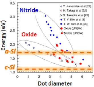
(TEM) images, shown as Fig. 1-11, the nano-crystalline Si QDs are clearly observed in the Si-rich nitride (SRN) layers [13]. Based on photoluminescence (PL) spectra analysis, the Eg,QD can be obtained. The measured PL peak energies from M. A.
Green’s and others’ results as a function of QD size are shown in Fig. 1-12 [13]. It clearly indicates the Eg,QD can be modified even larger than that of amorphous Si
material (~1.7 eV) by tuning the QD size. Hence, it demonstrates that the bandgap engineering is really a feasible idea by utilizing the Si QDs.
Fig. 1-10: Illustration of the fabrication process for the Si QD thin films using a [SiO2/SRO]-ML structure. [13]
Fig. 1-11: (a) Low and (b) high magnification TEM images of the Si QD thin films using a Si3N4 matrix material. [13]
9
Fig. 1-12: Bandgap energy versus QD size using SiO2 and Si3N4 matrix materials from different groups’ works. [13]
In 2008, M. A. Green et al. also experimentally demonstrates the feasibility of SCs integrating Si QDs [15, 16]. They fabricate the n-type Si QDs embedded SiO2
thin films on p-type c-Si wafer, as shown in Fig. 1-13. The n-type Si QD thin film is consisted of 15 or 25 bilayers of SiO2 and P-doped (0.23 at. %) Si QDs with a SiO2
thickness of 1 or 2 nm. The nominal diameters of the Si QDs are 3, 4, 5 and 8 nm. The SC with 3 nm of Si QDs has the highest efficiency, with open-circuit voltage (Voc) of
556 mV, short-circuit current (Jsc) of 29.8 mA/cm2, fill factor (F. F.) of 63.8%, and
conversion efficiency of 10.6%. The internal quantum efficiency (IQE) of the fabricated SCs and corresponding absorption spectra of the Si QD thin films are shown in Fig. 1-14, the well-matched relation is clearly observed. The thicker the SRO layer, the larger the QDs’ size, which results in a smaller effective bandgap. These results indicate that the conversion efficiency of the fabricated hetero-junction SCs is indeed enhanced by integrating with Si QDs.
10
Fig. 1-13: Illustration of a n-type Si QDs/p-type c-Si SC. [16]
Fig. 1-14:Internal quantum efficiency (IQE) and corresponding absorption spectra of the fabricated n-type Si QDs/p-type c-Si SCs. [16]
Since a large difference of the conversion efficiency between the experimental result and the theoretical calculation result is observed [17], in 2009, M. A. Green et al. publish more results focusing on the Si QD uniformity, interfacial defects, built-in electrical field, etc, in order to find out the roots for this discrepancy and try to optimize this structure for higher conversion efficiency [18-20]. More results for this development are also reported by different groups after 2010. For example, S. H. Hong et al. studied the size-dependent photovoltaic (PV) properties and developed the
11
higher efficiency SCs integrating Si QDs by optimizing the B-doped concentration
[21]. However, the results reported by M. A. Green et al. for the all Si QD thin film SCs indicate that the contributions of photo-generated carriers from QDs are apparently limited because of the naturally high-resistance property of the Si-based dielectric matrix materials [22, 23]. Therefore, more advanced and detailed studies are still necessary to solve the various issues involved using the Si-based dielectric matrices.
1-3
Applications on Other Optoelectronic Devices
Except for SCs application, Si QDs have also been extensively studied and integrated into various opto-electronic devices such as light-emitting diodes (LEDs)
[24, 25], photodetectors [26], and nonvolatile memory device [27]. For example, LEDs with multi-color light emission properties using Si QDs had been successfully developed by Prof. G. R. Lin et al. [24, 25], and Prof. J. M. Shieh et al. had also integrated Si QDs into near-infrared field-effect transistor photo-detectors by using a metal-oxide-semiconductor (MOS) device structure [26] and nonvolatile memory devices by using a nanosecond laser spike annealing method [27]. Hence, they had exhibited the feasibility and shown the great potential for optoelectronic devices integrating Si QDs.
12
1-4
Motivation for Solar Cells Application
To summarize the key issues for SCs integrating Si QDs, the Si QD thin films require uniform QD size [21, 28], heavily-doped concentration [21], and smaller QD separation [28-30], that is, higher QD density, or a more suitable matrix material. So far, the Si QD thin films are commonly deposited by a silicon-rich oxide single-layer (SRO-SL) or a [silicon dioxide/silicon-rich oxide] multilayer ([SiO2/SRO]-ML)
structure. The SRO-SL structure is an easy and quick deposition process for the Si QD thin films, however, it is hard to well control the QD size and uniformity and efficiently reduce the QD separation [31, 32]. Although the [SiO2/SRO]-ML structure
promises the QD size control and separation reduction, shown as Fig. 1-15, the minimum thickness of 2 nm for the SiO2 barrier layers is required to prevent the
excess Si atoms in SRO active layers from over-diffusing [11], which will still degrade the carrier transport efficiency [28-30]. Hence, significantly smaller QD separation or other more suitable matrix materials [33] are indispensable for the Si-based SCs development integrating Si QDs.
Fig. 1-15: Illustration of the Si QD thin film fabricated by using a [SiO2/SRO]-ML deposition structure.
13
1-4.1 Si QD Thin Films Utilizing a Gradient Si-rich Oxide Multilayer (GSRO-ML) Structure
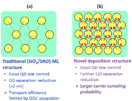
In order to further enhance the carrier transport efficiency, more QD separation reduction is required to significantly increase the carrier tunneling probability [28-30]. Fig. 1-16 shows an illustration of the carrier transport process for the Si QD thin films fabricated by using the traditional [SiO2/SRO]-ML and novel deposition structures.
The red lines mean the main carrier transport paths in both structures, and the thicker lines represent the larger tunneling probability. It indicates when the Si QD thin films with good QD size control and further QD separation reduction are successfully developed, the carrier tunneling probability will be significantly increased due to a narrower barrier width formation. Hence, a novel deposition structure, leading to the good QD size control and further QD separation reduction, can be very helpful for the Si-based SCs integrating Si QDs.
In this study, we propose to develop a novel deposition structure, gradient Si-rich oxide multilayer (GSRO-ML), for the Si QD thin films with good QD size control and QD separation minimization by co-sputtering deposition and high-temperature annealing methods, as shown in Fig. 1-17. Each GSRO period is composed of a highly SRO layer sandwiched between gradient SRO layers. In this proposed structure, the Si-rich atoms are anticipated to self-assemble and take the highly SRO regions as the crystallized centers during annealing due to the significant difference of Si/O composition, and the further reduced QD separation, also means the higher QD density, is expected to be formed after annealing.
14
Fig. 1-16: Illustrations of the main carrier transport process in the Si QD thin films fabricated by using
the (a) traditional [SiO2/SRO]-ML and (b) novel deposition structures. The thicker lines in (b) than that in (a) represent the larger tunneling probability obtained.
Fig. 1-17: Illustration of the Si QD thin film fabricated by using our proposed GSRO-ML deposition
structure.
1-4.2 Si QD Thin Films Utilizing ZnO Matrix Material
In addition to develop the GSRO-ML deposition structure for the Si QD thin films using the Si-based dielectric matrix materials, we also focus on developing a novel and more suitable matrix material since the characteristics of matrix material can obviously influence the electro-optical properties of the Si QD thin films. Fig. 1-18 shows an illustration of the carrier transport process in the Si QD thin films utilizing the insulated and semi-conductive matrix materials. Being different from
15
tunneling through QDs by using an insulated matrix material, more efficient transport paths may be contributed from using a semi-conductive matrix material for the Si QD thin films. Hence, we propose to embed Si QDs into ZnO thin films because ZnO has many desirable features to function as Si QDs’ matrix material, such as wide (~3.3 eV) and direct bandgap, high transparency, and highly tunable electrical properties [34]. And so far, only few materials can simultaneously possess these properties. Hence, ZnO can serve as the Si QDs’ matrix material for bandgap engineering, reduce the optical loss from matrix’s absorption, and efficiently enhance the carrier transport efficiency. Undoubtedly, there are many advantages to embed Si QDs in ZnO thin films for SCs application.
Fig. 1-18: Illustration of the main carrier transport process for Si QDs embedded in an (a) insulated or
(b) semi-conductive matrix material. The lines with different colors represent the different carrier transport paths.
16
1-5 Summary
The third generation SCs with high efficiency and low cost plays the indispensible roles for popularized developments. Si QD has the good ability on bandgap engineering to efficiently improve the mismatched photon energy loss, hence, the Si-based SCs integrating Si QDs can possess great potential on being as the third generation SCs. However, so far, the carrier transport efficiencies are still significantly limited by using the Si-based dielectric matrix materials due to their naturally high resistance properties. In this study, we propose to develop the novel Si QD thin films by utilizing a GSRO-ML deposition structure for further QD separation reduction and integrating with ZnO matrix material for better carrier transport path. The apparatus, sample fabrication, and characteristics for our proposed novel Si QD thin films are investigated and discussed in next chapters.
17
Chapter 2
Experimental Apparatus
In this chapter, the experimental apparatus for our samples fabrication and characteristics measurement for the novel Si QD thin films are introduced in detail and shown below.
2-1 Apparatus for Sample Fabrication
2-1.1 Wet-bench and Ultrasonic Cleaner
The Si(100) wafers and fused quartzes were used as substrates and cleaned in the wet bench before deposition, as shown in Fig. 2-1(a). The Si wafers were cleaned by a standard Radio Corporation of America (RCA) process to efficiently remove the organic contaminants (organic clean), the thin oxide layer (oxide strip), and the ionic contamination (ionic clean) [35, 36]. The fused quartzes were cleaned by an ultrasonic cleaner, shown as Fig. 2-1(b), the acetone, alcohol, and DI waters were in turn used as the cleaning solvents during ultrasonic oscillation process for 10 minutes individually
[37].
18
2-1.2 Radio-Frequency Magnetron Co-Sputtering System
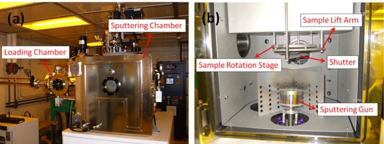
The Si QD thin films were deposited by using a radio-frequency (RF) magnetron co-sputtering system, the outside image is shown in Fig. 2-2(a). There are two chambers in this sputtering system including the sputtering and loading ones. The films deposition process is made in the sputtering chamber; the loading chamber is designed for quick sample transportation under keeping the high vacuum in the sputtering chamber. The inside image of this sputtering chamber is also shown in Fig. 2-2(b), it’s mainly composed of one sample lift arm, one sample rotation stage, four sputtering guns, and two shutters. The sample lift arm is installed for the sample transportation process between the sputtering and loading chambers. The sample holder is put on the sample rotation stage, which rotates at 15 r.p.m. during sputtering for uniform film deposition. The four sputtering guns are designed for the requirement of different sputtering materials during deposition. The two shutters are set up for the sample protection when the sputtering material is changed. In addition, the base pressure of this sputtering system was controlled at a high vacuum range of <5×10⁻⁷ torr for the good film quality obtained. Fig. 2-3 shows an illustration of the sputtering deposition process. In this study, the n-type Si QD embedded SiO2 thin films were
deposited by co-sputtering the P-doped Si and pure SiO2 materials, and the Si QD
embedded ZnO thin films were obtained by sputtering the intrinsic Si and ZnO materials individually.
19
Fig. 2-2: (a) Outside and (b) inside images of the RF magnetron co-sputtering system.
20 2-1.3 Furnace Annealing System
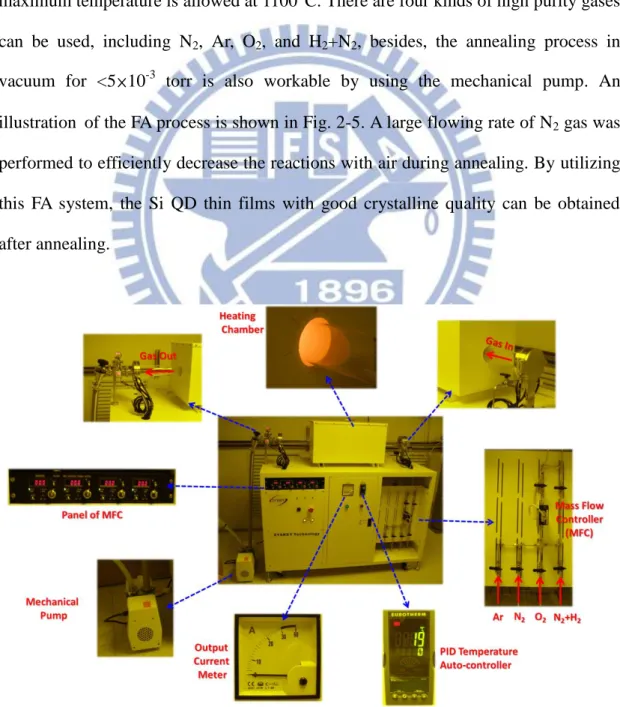
In order to obtain the nano-crystalline Si QDs formation, the as-deposited multilayer thin films were annealed by furnace annealing (FA). The images of the FA system and its main components, such as the proportional-integral-derivative (PID) temperature auto-controller, mass flow controller (MFC), heating chamber, mechanical pump, and entrance and exit of gas, are shown in Fig. 2-4. In this FA system, the temperature is auto-controlled by the PID temperature controller, and the maximum temperature is allowed at 1100°C. There are four kinds of high purity gases can be used, including N2, Ar, O2, and H2+N2, besides, the annealing process in
vacuum for <5×10⁻³ torr is also workable by using the mechanical pump. An illustration of the FA process is shown in Fig. 2-5. A large flowing rate of N2 gas was
performed to efficiently decrease the reactions with air during annealing. By utilizing this FA system, the Si QD thin films with good crystalline quality can be obtained after annealing.
21
Fig. 2-5: Illustration of a furnace annealing process.
2-1.4 Reactive Ion Etching System
For electrical properties measurements, the annealed samples for the Si QD embedded SiO2 thin films were etched by reactive ion etching (RIE) process with
CHF3 and O2 gases to remove the top SiO2 layers formed during annealing. The RIE
process was made by a SAMCO RIE200L system, which is supported from Nano Facility Center (NFC) in National Chiao Tung University (NCTU), shown as Fig. 2-6. An illustration of a RIE system and its etching process is shown in Fig. 2-7, it’s consisted of two electrodes (1 and 4) that create an electric field (3) meant to accelerate ions (2) toward the surface of the samples (5) [38]. The chemically reactive plasma is generated under low pressure by an electromagnetic field. Then, the high-energy ions from the plasma attack the sample surface and react with it, and the material on the sample surface will be removed during etching process [38].
22
Fig. 2-6: Image of the reactive ion etching system (RIE200L, SAMCO).
Fig. 2-7: Illustration of a reactive ion etching process. ((1) and (4): two electrodes, (2): F- ions, (3): electric field, (5): samples) [38]
23 2-1.5 Thermal Evaporator
For electrical properties measurements, the Al or Ni electrode layer with 100 nm thickness was deposited on the top and bottom surfaces of samples at room- temperature by thermal evaporator, shown as Fig. 2-8. The thermal evaporation process is also illustrated in Fig. 2-9 [39]. In this study, the base pressure during thermal evaporation was controlled at <4×10⁻⁶ torr. After electrode layers deposition, the samples were heated at 200°C in N2 environment for 20 minutes to form the good
ohmic contact.
Fig. 2-8: Image of the thermal evaporator.
24
2-2 Apparatus for Characterization Measurement
2-2.1 Micro-Raman Spectroscopy
The Raman spectra were measured by using a high-resolution confocal micro-Raman spectroscopy (Horiba LabRam HR) with a 488 nm diode-pumped solid-state laser, as shown in Fig. 2-10, it’s supported from Prof. Kien-Wen Sun’s laboratory at Centre of Nanoscience and Technology (CNST) in National Chiao Tung University (NCTU). An illustration of a micro-Raman spectroscopy and its measurement process are also shown in Fig. 2-11 [40].
Fig. 2-10: Image of the micro-Raman and micro-photoluminescence (PL) spectroscopy (Horiba
LabRam HR).
25 2-2.2 Micro-Photoluminescence Spectroscopy
The micro-photoluminescence (PL) spectra were measured by a Horiba LabRam HR, which is the same with the micro-Raman spectra measurements, and a 488 nm diode-pumped solid-state laser was also used as the excitation source. An illustration of a micro-PL spectroscopy is also shown in Fig. 2-12 [41].
26 2-2.3 X-Ray Diffractometer
The X-ray diffraction (XRD) patterns were examined by a high-resolution X-ray diffractometer (Bede, D1) with Cu Kα radiation, as shown in Fig. 2-13; it’s supported
from Centre of Nanoscience and Technology (CNST) in National Chiao Tung University (NCTU). In this study, the grazing incident X-ray diffraction (GIXRD) method, illustrated as Fig. 2-14, was used as the scan mode for the crystallization examinations of thin films [42]. During XRD measurements, the incident angle and the integration time were fixed at 0.5° and 2 seconds respectively.
Fig. 2-13: Image of the X-ray diffractometer (Bede D1).
27
2-2.4 Ultraviolet/Visible/Near-Infrared Spectroscopy
The optical transmission and reflection spectra were obtained using a variable-angle ultraviolet/visible/near-infrared (UV-VIS-NIR) spectroscopy (Hitachi U-4100) with an integrating sphere inner-coated by BaSO4, as shown in Fig. 2-15,
which is supported from Centre of Nanoscience and Technology (CNST) in National Chiao Tung University (NCTU). The measurement process of UV/VIS/NIR spectra is also illustrated in Fig. 2-16 [43].
Fig. 2-15: Image of the ultraviolet/visible/near-infrared spectroscopy (Hitachi U-4100).
28 2-2.5 Atomic Force Microscope
The surface morphologies were analyzed by a Digital Instrument D3100 atomic force microscope (AFM) shown as Fig. 2-17, it’s supported from Centre of Nanoscience and Technology (CNST) in National Chiao Tung University (NCTU). The detection of AFM images was designed as a beam deflection method, as shown in Fig. 2-18 [44], and the morphologies were scanned in a tapping mode.
Fig. 2-17: Image of the atomic force microscope (D3100).
29 2-2.6 Transmission Electron Microscope
The high-resolution transmission electron microscope (TEM) images were observed by a JEOL JEM-2010F TEM, as shown in Fig. 2-19, which is supported from National Nano Device Laboratories (NDL). An illustration of a TEM system with basic optical components is also illustrated in Fig. 2-20 [45]. The samples for TEM images were prepared by the conventional method, including the cutting, grinding, polishing, dimpling, and ion milling processes and thinned down to electron transparency using a precision ion polishing system (Gatan 691) shown as Fig. 2-21.
30
Fig. 2-20: Illustration of a transmission electron microscope. [45]
31
2-2.7 Semiconductor Device Measurement System
The dark and light current-voltage (I-V) curves were measured by a semi- conductor device measurement system shown as Fig. 2-22. Fig. 2-23 also shows the magnified images of the main components in this measurement system, it mainly involves an Agilent E5270B precision measurement mainframe, a measurement station, and a halogen light source. In the light I-V curves, an illumination with power density of ~1 mW/cm2 from the light source was used for the examinations of photoresponsive properties.
Fig. 2-22: Image of the semiconductor device measurement system.
Fig. 2-23: Images of the main components of the semiconductor device measurement system: (a)
measurement station, (b) Agilent E5270B precision measurement mainframe, and (c) halogen light source.
32 2-2.8 Solar Simulator Measurement System
The performances of our fabricated solar cells (Discussed in Appendix) were measured under one sun condition (Class A, AM1.5G) by a solar simulator measurement system (Newport), as shown in Fig. 2-24, which is supported from Prof. Pei-Chen Yu’s laboratory at Institute of Electro-Optical Engineering in National Chiao Tung University (NCTU). An illustration of the solar simulator measurement system is also illustrated in Fig. 2-25.
Fig. 2-24: Image of the solar simulator measurement system (Newport).
33 2-2.9 Quantum Efficiency Measurement System
The quantum efficiency (QE) spectra of our fabricated solar cells (Discussed in Appendix) were examined by a QE measurement system (Hitachi QE-3000) shown as Fig. 2-26, which is supported from Centre of Nanoscience and Technology (CNST) in National Chiao Tung University (NCTU). The measurement process for a QE system is also illustrated in Fig. 2-27 [46].
Fig. 2-26: Image of the quantum efficiency measurement system (Hitachi QE-3000).
34
Chapter 3
Si QD Thin Films Utilizing a Gradient Si-rich Oxide
Multilayer (GSRO-ML) Structure
In chapter 3, a novel deposition structure, gradient Si-rich oxide multilayer (GSRO-ML), was developed to further reduce QD separation for the Si QD embedded SiO2 thin films. Comparisons in the nano-structural, optical and electrical, and
photovoltaic (PV) properties between the Si QD thin films utilizing the commonly- used [SiO2/SRO]-ML structure and our proposed GSRO-ML structure were
investigated and discussed.
3-1 Sample Fabrication
The n-type GSRO-ML thin films were deposited on p-type Si(100) wafers with 1~10 ohm-cm in resistivity and fused quartzes at room-temperature by radio- frequency (RF) magnetron co-sputtering deposition method. Before deposition, the Si wafers and the fused quartzes were cleaned by the standard RCA and ultrasonic oscillation processes individually. The Si material with phosphorus doping concentration of ~1×1018 cm-3 and pure SiO2 material were used as the sputtering
targets. The sputtering power of Si (PSi) for each GSRO period was increased from 30
to 110 W at a rate of 1 W/s and hold at 110 W for 1 nm thickness, then decreased from 110 to 30 W also at a rate of 1 W/s while that of SiO2 (PSiO2) was fixed at 20 W, as
illustrated in Fig. 3-1.
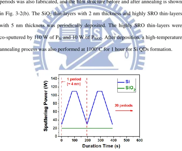
Fig. 3-2(a) shows the fabrication process of the GSRO-ML thin films with 20 periods before and after annealing. Each GSRO period is composed of a highly SRO layer sandwiched between gradient SRO layers for a total thickness of 4 nm during
35
deposition, and a super-high QD density is expected to be formed after annealing at 1100°C for 1 hour. For electro-optical properties measurements, the annealed samples were etched by reactive ion etching (RIE) process with CHF3 and O2 gases to remove
the top SiO2 layers formed during annealing. After RIE process, the Al electrodes
were deposited on the top and bottom surfaces of samples with 100 nm thicknesses by thermal evaporator, and a square electrode array with area of 0.8×0.8 mm2 and side-to-side separation of 1 mm was used as the top electrode distribution for photo-response measurements. For comparison, a [SiO2/SRO]-ML thin film with 20
periods was also fabricated, and the film structure before and after annealing is shown in Fig. 3-2(b). The SiO2 thin-layers with 2 nm thickness and highly SRO thin-layers
with 5 nm thickness was periodically deposited. The highly SRO thin-layers were co-sputtered by 110 W of PSi and 10 W of PSiO2. After deposition, a high-temperature
annealing process was also performed at 1100°C for 1 hour for Si QDs formation.
36
Fig. 3-2: Illustrations of film structures for samples (a) GSRO-ML and (b) [SiO2/SRO]-ML before and after annealing.
3-2 Nano-Crystalline and Structural Properties
Raman spectrum measurement is a reliable and widely-used technique for examining the properties of nano-crystalline Si (nc-Si) materials [47, 48]. Fig. 3-3 shows the Raman spectra of samples GSRO-ML and [SiO2/SRO]-ML, in which the
observed peaks near 520 cm-1 represent the nc-Si formation. In general, the signal can be decomposed into three components including the peaks located at ~480, 500~510, and 510~520 cm-1, which originate from the transverse optical (TO) modes of Si-Si vibrations in the amorphous- (a-Si), intermediate- (i-Si), and nano-crystalline Si (nc-Si) phases [47]. The curve-fitting results from Raman spectra are listed in Table 3-1. The similar FWHM values of nc-Si phase for both samples indicate the close average sizes of nc-Si [48]. However, sample GSRO-ML shows not only significantly larger nc-Si intensity but also higher Si crystal volume fraction (fc-Si) than those of sample
37
nc-Si with better crystal quality. Hence, compared with the commonly-used [SiO2/SRO]-ML structure, our proposed GSRO-ML structure can largely enhance the
nc-Si formation while maintaining the control ability of nc-Si size for the Si QD thin films.
Fig. 3-3: Raman spectra of samples GSRO-ML and [SiO2/SRO]-ML.
Table 3-1: Curve-fitting results from Raman spectra for the crystalline properties of samples GSRO-ML
and [SiO2/SRO]-ML.
Sample
TO mode of nc-Si phase Si crystal
volume fraction (fc-Si) (%) Peak position (cm-1) FWHM (cm-1)
Integrated intensity per nanometer in thickness (a.u.)
GSRO-ML 514.0 9.8 1.4×10² 73.0
[SiO2/SRO]-ML 516.3 9.7 1.2×101 68.4
Figs. 3-4(a) and (b) show the high-resolution TEM images of samples [SiO2/SRO]-ML and GSRO-ML. Most of Si QDs in sample [SiO2/SRO]-ML are
formed in SRO layers and separated by SiO2 barrier layers. For sample GSRO-ML, a
large number of Si QDs with closer separation is clearly observed, which indicates that a super-high density of Si QDs can be formed by using a GSRO-ML structure. Fig. 3-4(c) shows the corresponding QD size distributions from estimating 40 QDs in
38
samples [SiO2/SRO]-ML and GSRO-ML. Both samples reveal the similar QD size
distributions, mainly from 4 to 6 nm, and the close average QD sizes of ~5.2 and ~4.9 nm. However, the calculated QD density of ~3×1012 cm-2 for sample GSRO-ML is significantly higher than that of ~9×1011 cm-2 for sample [SiO2/SRO]-ML, which is
close to the QD density calculated from the reports by G. Conibeer et al. and M. Zacharias et al. [10, 11]. Therefore, the Si QD thin film using a GSRO-ML structure shows excellent capabilities on not only the QD size control but also the super-high QD density formation, and such results are very helpful for SCs application integrating Si QDs.
Fig. 3-4: High-resolution TEM images of samples (a) [SiO2/SRO]-ML and (b) GSRO-ML. (c) The corresponding QD size distributions.
39
3-3 Photoluminescence Emission and Optical Absorption Properties
The effective bandgap and light emission properties of the Si QD thin films have been widely investigated by photoluminescence (PL) spectrum [49-51]. The main PL emissions are from the quantum confinement (PLQC) effect accompanying with thecarrier recombinations from the interface defect states between Si QDs and SiO2
matrix (PLD-interface) and the defect states in SiO2 matrix (PLD-SiO2) [49-51]. Fig. 3-5
shows the PL spectra and the fitting curves of samples GSRO-ML and [SiO2/SRO]-ML, and the curve-fitting results are given in Table 3-2. The broad PL
emission properties are observed in both samples, and they can be nicely decomposed into three components, contributed from PLQC, PLD-interface, and PLD-SiO2. The effective
bandgap obtained from the peak position of PLQC in sample GSRO-ML is a little
larger than that in sample [SiO2/SRO]-ML, mainly owing to the slightly smaller
average QD size [11], but not the closer QD separation, which will lead to an energy red shift [30]. In addition, sample GSRO-ML, with higher QD density, exhibits a considerably lower PLQC intensity than that of sample [SiO2/SRO]-ML. This indicates
that more photo-generated carriers can transport through QDs rather than recombine inside QDs during PL spectrum measurement since the QD separation is significantly reduced. The increased PLD-SiO2 in sample GSRO-ML is a reasonable result because
the all Si-rich oxide matrix is used and more Si excess atoms will be left behind inside the SiO2 matrix after Si QDs formation [51]. Since a suitable number of defect states
inside SiO2 matrix can improve the carrier transport efficiency for the Si QD thin films
[28, 52], the Si QD thin film using a GSRO-ML structure is more advantageous for SCs application. Therefore, the PL measurement results of the Si QD thin film using the proposed GSRO-ML structure with super-high QD density and good QD size control reveal the better properties and the capability of effective bandgap engineering even though the Si QDs are closely formed.
40
Fig. 3-5: PL spectra and the fitting curves of samples GSRO-ML and [SiO2/SRO]-ML.
Table 3-2: Curve-fitting results from PL spectra of samples GSRO-ML and [SiO2/SRO]-ML.
Sample
Defect states in SiO2
matrix (D-SiO2)
Quantum confinement effect (QC)
Interface defect states (D-interface) Peak position Intensity (a.u.) Peak position Intensity (a.u.) Peak position Intensity (a.u.) GSRO-ML 2.15 eV (577 nm) 8.0×10⁴ 1.76 eV (705 nm) 4.6×10⁴ 1.52 eV (816 nm) 1.5×10³ [SiO2/SRO]-ML 2.05 eV (604 nm) 1.4×10⁴ 1.68 eV (740 nm) 3.7×10⁵ 1.46 eV (848 nm) 6.0×10⁴
To further confirm the cause of the reduced PLQC emission in sample GSRO-ML,
Fig. 3-6 shows the I-V curves of samples GSRO-ML and [SiO2/SRO]-ML with and
without a 488 nm laser illumination, which is used for PL spectrum measurements. A much more obvious ISC enhancement is observed in sample GSRO-ML than that in
sample [SiO2/SRO]-ML in the light I-V curves. This verifies that the reduced PLQC
emission in sample GSRO-ML is mainly caused by the better carrier transport properties resulting from the closer QD separation than that in sample [SiO2/SRO]-ML.
41
Fig. 3-6: I-V curves of samples GSRO-ML and [SiO2/SRO]-ML with and without a 488 nm laser illumination.
In order to understand the optical absorption properties of samples GSRO-ML and [SiO2/SRO]-ML, the absorption spectra are measured and shown in Fig. 3-7. The
absorption coefficient of sample GSRO-ML is clearly larger than that of sample [SiO2/SRO]-ML owing to the higher QD density. Inset of Fig. 3-7 shows the Tauc plot
for indirect allowed transition. The optical bandgap (Eg,opt) can be evaluated by linear
extrapolating the interception at the energy axis (αhν=0) from the plot of (αhν)1/2
as a function of incident photon energy (hν), where α is the optical absorption coefficient
[53]. The obtained Eg,opt of samples GSRO-ML and [SiO2/SRO]-ML are 1.96 and 1.83
eV, and the corresponding α values are 3.4×10³ and 3.1×102 cm-1. The slightly larger Eg,opt of sample GSRO-ML than that of sample [SiO2/SRO]-ML matches with the
obtained results of effective bandgap from PLQC emission, which is contributed from
the little difference in average QD size. Furthermore, the α value of sample GSRO-ML is significantly improved to be over 10 times larger than that of sample [SiO2/SRO]-ML and close to that of amorphous Si material [54]. This means the Si
QD thin films using a GSRO-ML structure can contribute the better photo-responsive property and largely reduce the required film thickness for SC applications. Therefore,
42
our proposed GSRO-ML structure makes the Si QD thin film more practical and potential for the commercial SCs development.
Fig. 3-7: Absorption spectra of samples GSRO-ML and [SiO2/SRO]-ML. Inset shows the corresponding Tauc plots for indirect allowed transition.
3-4 Photovoltaic Properties and Carrier Transport Mechanism
Fig. 3-8 shows the illustration of the device structure for I-V measurements and the dark and light I-V curves of samples GSRO-ML and [SiO2/SRO]-ML. Both
samples reveal the rectification behavior as a diode. However, the better I-V characteristics including a lower turn-on voltage and a higher forward current are obtained in sample GSRO-ML. Inset of Fig. 3-8(b) shows the corresponding light I-V curves under a halogen lamp illumination with ~1 mW/cm2 of power density. The VOC
and ISC for sample GSRO-ML are 302 mV and 5.5×10⁻⁴ mA, significantly larger than
110 mV and 2.6×10⁻⁵ mA for sample [SiO2/SRO]-ML. Hence, the PV properties of the
43
Fig. 3-8: (a) Illustration of the device structure for I-V measurements and (b) the dark I-V curves of
samples GSRO-ML and [SiO2/SRO]-ML. Inset shows the corresponding light I-V curves under a halogen lamp illumination.
To investigate the carrier transport mechanism, the dark forward I-V curves of samples [SiO2/SRO]-ML and GSRO-ML are plotted on a log-log and shown in Fig.
3-9. For sample [SiO2/SRO]-ML, the combination of the direct and phonon-assisted
tunneling mechanisms is fitted with the experimental result, which is consistent with the conclusion from V. Osinniy et al. [55]. For sample GSRO-ML, instead of the direct and phonon-assisted tunneling mechanisms, the two-diode mode is more appropriate to describe its forward current [56]. The current increases linearly with the bias in low bias region (region I, V < 0.3 V), exponentially with the bias in the intermediate bias region (region II, V = 0.3~1.5 V), and deviates from exponential behavior in the higher bias region (region III, V > 1.5 V). The clearly distinct conductive regions indicate a corresponding change in the dominating carrier transport mechanism. The two-diode mode had also been observed by S. Park et al. from the heavily P-doped Si QD thin films integrated with B-doped Si wafer [56]. The linear relationship between log I and log V in region I indicates the presence of a parallel current path due to a shunt resistor in parallel to the junction. In region II, a feature of the current exponentially increasing with bias is dominated by the space-charge region recombination mechanism. In region III, the cause of the I-V characteristics deviated
![Fig. 1-10: Illustration of the fabrication process for the Si QD thin films using a [SiO 2 /SRO]-ML structure](https://thumb-ap.123doks.com/thumbv2/9libinfo/8512658.185956/27.892.151.737.433.1007/fig-illustration-fabrication-process-films-using-sio-structure.webp)
![Fig. 1-15: Illustration of the Si QD thin film fabricated by using a [SiO 2 /SRO]-ML deposition structure](https://thumb-ap.123doks.com/thumbv2/9libinfo/8512658.185956/31.892.134.753.439.1006/fig-illustration-film-fabricated-using-sio-deposition-structure.webp)
![Fig. 3-2: Illustrations of film structures for samples (a) GSRO-ML and (b) [SiO 2 /SRO]-ML before and after annealing](https://thumb-ap.123doks.com/thumbv2/9libinfo/8512658.185956/55.892.142.759.133.874/fig-illustrations-film-structures-samples-gsro-sio-annealing.webp)
