國 立 交 通 大 學
電子工程學系 電子研究所碩士班
碩 士 論 文
應用於低溫多晶矽製程下和差類比數位轉換器
電路設計與實現
Design and Realization of Delta-Sigma
A/D Converter in LTPS Technology
研 究 生: 蔡佳琪 (Chia-Chi Tsai)
指導教授: 柯明道教授 (Prof. Ming-Dou Ker)
應用於低溫多晶矽製程下和差類比數位轉換器
電路設計與實現
Design and Realization of Delta-sigma
A/D Converter in LTPS Technology
研 究 生:蔡佳琪 Student:
Chia-Chi
Tsai
指導教授:柯明道教授
Advisor:
Prof.
Ming-Dou
Ker
國立交通大學
電子工程學系
電子研究所
碩士論文
A Thesis
Submitted to Department of Electronics Engineering and Institute of Electronics
College of Electrical and Computer Engineering
National Chiao-Tung University
in Partial Fulfillment of the Requirements
for the Degree of
Master
in
Electronics Engineering
March 2009
Hsin-Chu, Taiwan
中華民國九十八年三月
~ i ~
應用於低溫多晶矽製程下
和差類比數位轉換器電路設計與實現
學生:蔡佳琪
指導教授:柯明道教授
國立交通大學
電子工程學系電子研究所碩士班
ABSTRACT (CHINESE)
低 溫 複 晶 矽 (low temperature polycrystalline silicon, LTPS) 薄膜電晶體 (thin-film transistors, TFTs) 已被視為一種材料廣泛地研究於可攜帶式系統產品 中,例如數位相機、行動電話、個人數位助理 (PDA) 、筆記型電腦等,這是由 於低溫複晶矽薄膜電晶體的電子遷移率約是傳統非晶矽 (amorphous silicon) 薄 膜電晶體的一百倍大。此外,低溫複晶矽技術可藉由將驅動電路整合於顯示器之 周邊區域來達到輕薄、巧小且高解析度的顯示器。這樣的技術也將越來越適合於 系統面板 (System-on-Panel, SOP) 應用之實現。
隨著系統面板的發展,各式輸入顯示技術 (input display technology) 被整合 於其中,包含了記錄文字、影像或是照片的掃描器 (scanner) ,偵測手指或是筆 跡的觸控式面板 (touch panel) 等,這些新穎的應用不管對於個人或是企業都可 以帶來很大的便利性。另外,面板溫度對液晶顯示器薄膜電晶體影響顯著,因此 為了提升系統可靠度,溫度補償電路也廣泛的被討論。無論是在觸控式面板設計 抑或是溫度補償電路等,其中都包含了感測電路 (sensing circuit) 。類比至數位 轉換器就是一種被廣泛地應用在感測電路後端,將感測到的類比訊號轉換為數位 訊號進而驅動其它數位訊號處理器 (DSP) 的電路。因此,隨著輸入顯示技術的 發展以及溫度補償電路的不可或缺性,面板上類比至數位轉換器的整合是非常值 得被研究與探討。
~ ii ~
在本篇論文之中,首次提出了設計於玻璃基板上之和差類比至數位轉換電路 並且已經在三微米低溫複晶矽薄膜電晶體製程下成功被驗證。相較於其它類比至 數位轉換器 (flash ADC, pipeline ADC),此電路可藉由負迴授機制以操作速度換 取較高的解析度,同時佔用較小的面積。此類比至數位轉換器操作在十伏特的操 作電壓之下,前端和差調變器 (delta-sigma modulator) 將類比輸入訊號轉換成連 續性的位元流 (bit stream),再經由降頻濾波器 (decimation filter) 轉換為八位元 之數位訊號。此新提出的類比至數位轉換器電路未來將可以被整合在面板上,帶 來更便利性的應用。
~ iii ~
Design and Realization of Delta-Sigma
A/D Converter in LTPS Technology
Student: Chia-Chi Tsai
Advisor: Prof. Ming-Dou Ker
Department of Electronics Engineering &Institute of Electronics
College of Electrical and Computer Engineering
National Chiao-Tung University
ABSTRACT (ENGLISH)
Low temperature polycrystalline silicon (LTPS) thin-film transistors (TFTs) have been widely investigated as a material for portable systems, such as digital camera, mobile phone, personal digital assistants (PDAs), notebook, and so on, because the electron mobility of LTPS TFTs is about 100 times larger than that of the conventional amorphous silicon TFTs. Furthermore, LTPS technology can achieve slim, compact, and high-resolution display by integrating the driving circuits on peripheral area of display. This technology will also become more suitable for realization of System-on-Panel (SOP) applications.
SOP displays are value-added displays with various functional circuits, and the input display technology creates opportunities for new applications like a scanner for recording of text or images for on-line shops and touch-sensing circuits for detecting the position of finger or pen. Besides, optical characteristics of TFT-LCDs are significantly dependent on panel temperature. For wide usage in thermally harsh environments, LCD should use a robust temperature compensation system to enhance
~ iv ~
reliability and maintain performance. Sensing circuits are indispensable to these novel applications. The technique of forming an optical sensor using LTPS TFT fabrication process is developed to incorporate these new functions in the display without any additional circuit behind the display.
A/D converters (ADC) are widely used in the interface between analog sensing circuits and digital processing circuits to convert the analog sensor signals to a digital signal and then processed by some digital circuits or FPGA. For the above reason, integration of ADC on the glass substrate is my focus in this thesis.
In this thesis, a delta-sigma ADC designed and implemented with the TFTs on glass substrate has been proposed, and successfully verified in a 3-μm LTPS process. From the experimental results, the probability in the bit stream of the digital output from the delta-sigma modulator is correctly fit in the analog input voltage ratio. Such a bit stream can be converted into 8-bit digital code successfully under the operation voltage of 10V with TFTs on the glass substrate. The proposed delta-sigma ADC can be further used to achieve the precise analog circuits for SOP applications, which enables the analog circuits to be integrated in the active matrix LCD (AMLCD) panels.
~ v ~
ACKNOWLEDGEMENTS
致謝
在這兩年的碩士生涯當中,首先我要感謝的是我的指導教授 柯明道老師。 老師在接了義守大學副校長職位之後變得越來越忙碌,卻總是不辭辛苦的南北兩 地奔波,在每個星期一晚上回到新竹跟同學們開會,即使開會開到半夜十二點、 一點,老師卻仍精神奕奕,一點也看不出疲態,但想必是非常辛苦的吧! 而在我的研究過程中,我要特別感謝「友達光電股份有限公司」給予我們研 究群許多下線機會,讓我們有機會對我們的電路做一個很好的驗證。另外,我最 要感謝的是服務於其中的鯉魚學長。鯉魚學長在兩年前畢業於柯明道教授研究 群,之後便投入了友達光電。鯉魚學長不僅在研究上非常認真、知識非常富足, 他更是一個非常願意給予學弟妹幫助與指導的學長。尤其是在每次要下線之前, 即使學長手頭有非常多的工作,他仍願意為我們撥出時間做 DRC 及 LVS 驗證,每 次一忙下來可能就是一個上午,但他卻連一杯飲料都不希望給我們請,真的讓我 們大家都非常非常的感謝。 我還要感謝的是吳介琮老師研究群的金毛學長以及愛莉絲學長,謝謝你們對 於我研究以及量測的指導。對於這個研究題目我可以說是從無到有,常常碰壁。 謝謝你們對於不是同指導教授的我可以這麼不厭其煩的提點,每當我有一個問題 出現的時候,學長們卻總是舉一反三,幫助我建立更完整的概念。 此外,我要感謝的是「奈米與晶片系統實驗室」的學長姐及學弟妹們,在各 方面給予我協助,讓我可以順利完成我的畢業論文。 接著謝謝天天在我煩躁的時候讓我沒事踢踢他的椅子卻從不生氣、謝謝小州 哥在我小咪生不出來的時候半小時搞定同時為了我的破英文煩惱不已、謝謝小昀 昀提供美肌相機讓女孩們出遊總是拍拍拍的很開心還帶來了可愛的便便鼠、謝謝 世範在咪停的時候陪我聊天聊地聊是非、謝謝北鴨每次都提供好吃的甜點還親自 送來、謝謝吃吃跟狗達代替了北鴨跟我們可以多陪小州哥一年,謝謝實驗室的大 家,一起研究,一起玩樂,豐富了碩士班期間的生活。 另外,我要謝謝我的室友們,謝謝嚕嚕每天晚上陪我聊天聊到不用睡覺偶爾 還可以吃到親手做的美味早餐、謝謝南西口試前貼心的給我小卡片讓我更有信 心、謝謝青玉週末大家都不在的時候煮飯給我吃填飽我的肚子、謝謝蔣灣在下雨 天時都貼心的找我讓我搭便車,謝謝妳們讓我的外宿生涯每天開開心心。 最後,我最是要感謝的是我的父親蔡德根先生、哥哥蔡政偉以及我的男友陳 鞏鞏。我的父親對我們的愛是不可言喻的,他可以粗衣節食卻希望給我們好的生 活,他忙碌到生病卻不希望我們替他擔心,現在我畢業了,希望可以跟哥哥一起 努力,讓父親可以無憂無慮的生活。而男友不論開心或是難過,總是站在我的身 邊支持著我,走過好多好多個年頭,希望未來我們依然可以相互支持、開開心心 的走下去。~ vi ~ 要感謝的人太多了,若有遺漏,在此一併謝過。本論文撰寫時已力求嚴謹, 然謬誤之處在所難免,尚祈各位讀者不吝惜賜予寶貴意見,使本論文能更加完善。 蔡 佳 琪 僅誌於竹塹交大 民國九十八年三月
~ vii ~
CONTENTS
ABSTRACT (CHINESE) ... i
ABSTRACT (ENGLISH) ... iii
ACKNOWLEDGEMENTS ... v
CONTENTS ... vii
TABLE CAPTIONS... ix
FIGURE CAPTIONS ... x
Chapter 1 ... 1
Introduction ... 1
1.1 Motivation ... 11.1.1 LCD Industry and LTPS Technology [1], [2] ... 1
1.1.2 The Advantages of the System-on-Panel LTPS TFT-LCD Displays [4], [5] ... 2
1.1.3 Future Applications of “Input Display” [7] ... 7
1.1.4 Thermal Influence on LCDs [8], [9], [10] ... 11
1.1.5 Summary ... 12
1.2 Background Knowledge of Thin-Film Transistors Liquid Crystal Displays . 13 1.2.1 Brief Introduction of Liquid Crystal Displays [11], [12] ... 13
1.2.2 Liquid Crystal Display Module Structure ... 16
1.3 Thesis Organization ... 17
Chapter 2 ... 18
Fundamentals and Realization of
First-order Delta-sigma Modulator ... 18
2.1 Introduction ... 18
2.1.1 Nyquist-rate and Oversampled Converter [18] ... 18
2.1.2 Fundamentals of the First-order Delta-sigma Modulator [16], [18] ... 19
2.2 Circuits Implementation on Glass Substrate ... 23
2.2.1 Design of Fully-differential Folded-cascode Operational Amplifier .. 24
2.2.2 Design of 1-bit Quantizer... 27
~ viii ~
2.2.4 Summary ... 31
Chapter 3 ... 36
Decimation Filter for First-order
Delta-sigma Modulator ... 36
3.1 Introduction ... 36
3.2 Circuits Implementation on Glass Substrate ... 38
3.2.1 Design of the Counter ... 39
3.2.2 Design of the Register ... 42
3.2.3 Design of the Divider ... 43
3.2.4 Summary ... 45
3.3 Summary ... 46
Chapter 4 ... 47
Measured Results of the First-order Delta-sigma A/D Converter ... 47
4.1 Layout Considerations ... 47
4.2 Measured Results ... 49
4.2.1 Measurement Setup ... 49
4.2.2 Measured Results of the Delta-sigma Modulator ... 51
4.2.3 Measured Results of the Decimation Filter ... 55
4.2.4 Measured Results of the Delta-sigma A/D Converter ... 56
4.2.5 Summary ... 59
Chapter 5 ... 60
Conclusions and Future Works ... 60
5.1 Conclusions ... 60
5.2 Future Works ... 60
REFERENCES ... 62
VITA ... 64
~ ix ~
TABLE CAPTIONS
Table 2.1 The operation of delta-sigma modulator with an input signal x[n] of 6V. ... 23 Table 2.2 The probability of ‘logic-1’ in one period is calculated and listed as Vi+ is 8V. ... 32 Table 2.3 The probability of ‘logic-1’ in one period is calculated and listed as Vi+ is 7V. ... 33 Table 2.4 The probability of ‘logic-1’ in one period is calculated and listed as Vi+ is 5V. ... 34 Table 2.5 The probability of ‘logic-1’ in one period is calculated and listed as Vi+ is 3V. ... 35 Table 3.1 The truth table of the JK Flip-flop. ... 40
~ x ~
FIGURE CAPTIONS
Figure 1.1 System integration roadmap of LTPS TFT-LCD. ... 3 Figure 1.2 Basic concept of pixel memory technology. ... 4 Figure 1.3 (a) The schematic illustration of the “sheet computer” concept and (b) a CPU with an instruction set of 1-4 bytes and an 8-bit data bus on glass substrate. ... 4 Figure 1.4 The roadmap of LTPS technologies leading toward the realization of sheet computers. ... 5 Figure 1.5 Schematic cross-section view of the structure of a LTPS complementary metal oxide semiconductor (CMOS). LDD = lightly doped drain. ... 5 Figure 1.6 Comparison of (a) an amorphous silicon TFT-LCD module and (b) a low-temperature polycrystalline silicon TFT-LCD module. ... 6 Figure 1.7 The comparison of new SOP technology product and conventional product. The new 3.8” SOP LTPS TFT-LCD panel has been manufactured by SONY corp. in 2002. ... 7 Figure 1.8 Future applications of “Input Display”... 9 Figure 1.9 The principle and structure of the photo-sensing display. ... 9 Figure 1.10 The system architecture and image-capturing finger of the new touch panel. ... 10 Figure 1.11 TAD (Thermally adaptive driving) integrated thermal sensor system architecture. ... 11 Figure 1.12 The temperature readout circuit consists of an external full bridge circuit and a differential amplifier. ... 12 Figure 1.13 (a) A couple of polarizers with 90° phase error. (b) A couple of polarizers with liquid crystals. ... 14 Figure 1.14 The structure of a TN-LCD (a) while light is passing, and (b) while light is blocked. a: polarizer; b: glass substrate; c: transparent electrode; g: orientation layer; e: liquid crystal; f: illumination... 15 Figure 1.15 The cross section structure of TFT-LCD panel. ... 16 Figure 2.1 Basic circuit diagram of Delta-sigma ADC consists of delta-sigma
modulator and decimation filter. ... 20 Figure 2.2 Block diagram of delta-sigma modulator. ... 20 Figure 2.3 Circuit implementation of the delta-sigma modulator on glass substrate in a 3-μm LTPS technology. ... 24 Figure 2.4 Circuit implementation of the fully-differential folded-cascode operational amplifier on glass substrate in a 3-μm LTPS technology. ... 26 Figure 2.5 The simulated frequency response of the fully differential operational
~ xi ~
amplifier in open-loop condition. ... 26 Figure 2.6 Circuit implementation of the 1-bit quantizer on glass substrate in a 3-μm LTPS technology. ... 28 Figure 2.7 Time relation between φ1 and φ2. ... 28
Figure 2.8 The simulated result of the 1-bit quantizer. ... 29 Figure 2.9 Circuit implementation of the D flip-flop on glass substrate in a 3-μm LTPS technology. ... 30 Figure 2.10 The simulated result of the D flip-flop. ... 30 Figure 2.11 The simulated result of the first-order delta-sigma modulator when the input Vi+ is 8V. ... 32 Figure 2.12 The simulated result of the first-order delta-sigma modulator when the input Vi+ is 7V. ... 33 Figure 2.13 The simulated result of the first-order delta-sigma modulator when the input Vi+ is 5V. ... 34 Figure 2.14 The simulated result of the first-order delta-sigma modulator when the input Vi+ is 3V. ... 35 Figure 3.1 Diagram shows the input/output variables of the decimation filter. ... 36 Figure 3.2 Block diagram of decimation filter composed of a counter, register, and a divider. ... 38 Figure 3.3 The timing chart represents the relation between the Clk, Clk_N, and the output signal y of the decimation filter. ... 39 Figure 3.4 The circuit implementation of the JK Flip-flop which comprises of some logic gates and two SR_latches. ... 39 Figure 3.5 The block diagram of the counter built up with the JK Flip-flop and
controlled by the Clk and Clr signals where the input signal is b[n] and the output signal is c0-c7. ... 41
Figure 3.6 The timing chart of the counter as b[n] is high where the only least 3 significant bits are shown... 42 Figure 3.7 The block diagram of the register which consists of 8 D flip-flops which is positive edge triggered by the Clk signal. ... 43 Figure 3.8 The block diagram of the divider which consists of 8 D flip-flops. ... 44 Figure 3.9 Timing chart of the divider. ... 45 Figure 3.10 Timing chart of the decimation filter where its operation is divided into 5 steps and identified here... 46 Figure 4.1 The layout view of the operational amplifier used in the integrator of the delta-sigma modulator. ... 48 Figure 4.2 Die photo of the fabricated delta-sigma ADC in a 3-μm LTPS technology. ... 48
~ xii ~
Figure 4.3 The measurement setup illustration for delta-sigma modulator and the ADC with DC probing station. ... 50 Figure 4.4 The measurement setup illustration for decimation filter and the ADC with DC probing station. ... 50 Figure 4.5 Measured result of the delta-sigma modulator between the relation of output bit stream b[n] and clock signal Clk as the input Vi+ is 1V and Vi- is 9V. ... 51 Figure 4.6 Measured result of the delta-sigma modulator between the relation of output bit stream b[n] and clock signal Clk as both input Vi+ and Vi- are 5V. ... 52 Figure 4.7 Measured results of the fabricated delta-sigma modulator, comparing with the ideal calculation. ... 53 Figure 4.8 Comparison between ideal and measurement results of probability of ‘logic-1’ in the bit stream b[n] with different 10 panels. ... 53 Figure 4.9 Measured results comparison between the average of the 10 panels and the ideal one. ... 54 Figure 4.10 Standard deviation calculated between 10 panels with the input signal Vi+ changing from 1V to 9V. ... 54 Figure 4.11 Measured results of the decimation filter and its input signal is given by the pulse generator instead of the delta-sigma modulator. ... 55 Figure 4.12 Measured results of the ADC where its digital output is normalized to compare with the probability of b[n]. ... 57 Figure 4.13 Measured results of the ADC where its digital output is normalized to compare with the probability of b[n] with another panel. ... 57 Figure 5.1. Block diagram of the temperature sensor. ... 61
~ 1 ~
Chapter 1
Introduction
1.1 Motivation
1.1.1 LCD Industry and LTPS Technology [1], [2]
The liquid-crystal display (LCD) industry has shown rapid growth in five market areas, namely, notebook computers, monitors, mobile equipment, mobile telephones, and televisions. For high-speed communication networks, the emerging portable information tools are expected to grow in following on the rapid development of display technologies. Thus, the development of higher specification is demanded for LCD as an information display device. Moreover, the continual growth in network infrastructures will drive the demand for displays in mobile applications and flat panels for computer monitors and TVs. The specifications of these applications will require high-quality displays that are inexpensive, energy-efficient, lightweight, and thin.
Amorphous silicon (a-Si) thin-film transistors (TFTs) are widely used for flat-panel displays. However, this low field-effect mobility (ability to conduct current) property limits their application only as pixel switching devices; they cannot be used for complex circuits. Thus, the excimer laser annealing (ELA) process is established for manufacturing of polycrystalline Si (poly-Si) TFTs. The laser annealed polycrystalline silicon has relatively larger grain size and relatively exhibits higher electron and hole mobility functions than the conventional ones. The field-effect mobility of the poly-Si TFTs is about 100 times of the a-Si. The high driving ability of poly-Si TFTs allows the integration of various circuits such as display drivers. For example, to date the function of the external ICs which is used for driving the pixel
~ 2 ~
directly is integrated onto the peripheral of the glass substrate. It yields a lighter and thinner display with a drastic reduction of connection pins. It also improves the reliability against the mechanic shock as well as relaxes the limit in the pitch between connection terminals to be suitable for high resolution display. Thus, eliminating LSI (large-scale integration) chips for display drivers will decrease the cost and thickness of displays for various applications. Moreover, high driving ability of poly-Si can provide larger aperture ratio because poly-Si TFTs can drive the same current as a-Si TFTs but only occupy small space.
There are high-temperature and low-temperature poly-Si (HTPS and LTPS) TFTs, defined by the maximum process temperature they can withstand. The process temperature for high-temperature poly-Si can be as high as 900°C. Hence, expensive quartz substrates are required, and the profitable substrate size is limited to around 6 inch (diagonal). Typical applications are limited to small displays. The process temperature for low-temperature poly-Si (LTPS) TFTs, on the other hand, is less than 600°C, which would allow the use of low-cost glass substrates. This makes possible direct-view large-area displays—for example, UXGA (ultra extended graphics array) monitors of up to 15.1 inch (diagonal) with a resolution of 1600 x 1200 pixels. For this reason, LTPS technology has been applied successfully to not only small-sized displays, but also medium- and large-screen products. It is the base for high performance TFTs for active matrix liquid crystal displays.
1.1.2 The Advantages of the System-on-Panel LTPS TFT-LCD Displays [4], [5]
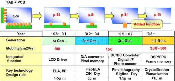
LTPS TFT technology of forming a part of display circuits on the glass substrate has been put into practical use. It can make a compact, high reliable, high resolution display. Because of this property, LTPS TFT-LCD technology is widely used for mobile displays. Fig. 1.1 shows the system integration roadmap of LTPS TFT-LCD
~ 3 ~
[3], [4], [5].
System-on-Panel (SOP) displays are value-added displays with various functional circuits, including static random access memory (SRAM) in each pixel, integrated on the glass substrate. Fig. 1.2 shows the basic concept of pixel memory technology. When SRAMs and a liquid crystal AC driver are integrated in a pixel area under the reflective pixel electrode, the LCD is driven by only the pixel circuit to display a still image. It means that no charging current to the data line for a still image. This result is more suitable for ultra low power operation.
Eventually, it may be possible to combine the keyboard, CPU, memory, and display into a single “sheet computer”. The schematic illustration of the “sheet computer” concept and a CPU with an instruction set of 1-4 bytes and an 8-bit data bus on glass substrate are shown in Fig. 1.3, respectively [1], [6]. Fig. 1.4 shows the roadmap of LTPS technologies leading toward the realization of sheet computers. Finally, all of the necessary function will be integrated in LTPS TFT-LCD. Although the level of LTPS is as almost the same as the level of the crystal Si of 20 years ago, actual operation of 50MHz with 1-μm design will be realized near future [7].
~ 4 ~
Figure 1.2 Basic concept of pixel memory technology.
Figure 1.3 (a) The schematic illustration of the “sheet computer” concept and (b) a CPU with an instruction set of 1-4 bytes and an 8-bit data bus on glass substrate.
~ 5 ~
Figure 1.4 The roadmap of LTPS technologies leading toward the realization of sheet computers.
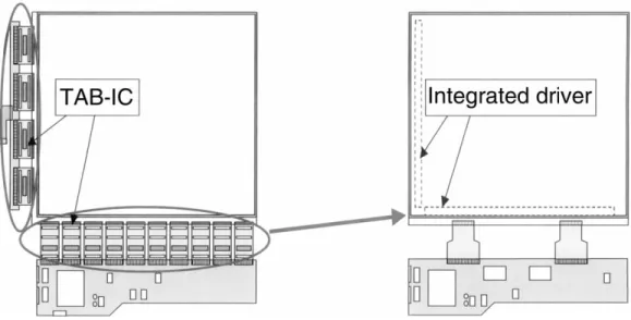
The distinctive feature of the LTPS TFT-LCD is the elimination of TAB-ICs (integrated circuits formed by means of an interconnect technology known as tape-automated bonding). LTPS TFTs can be used to manufacture complementary metal oxide semiconductors (CMOSs) in the same way as in crystalline silicon metal oxide semiconductor field-effect transistors (MOSFETs). Fig. 1.5 shows the cross sectional structure of a LTPS TFT CMOS.
Figure 1.5 Schematic cross-section view of the structure of a LTPS complementary metal oxide semiconductor (CMOS). LDD = lightly doped drain.
~ 6 ~
For a-Si TFT-LCDs, TAB-ICs are connected to the left and bottom side as the Y driver and the X driver, respectively. Integration of the Y and X drivers with LTPS TFTs requires PCB (printed circuit board) connections on the bottom of the panel only. The PCB connection pads are thus reduced to one-twentieth the size of those in a-Si TFT-LCDs. The most common failure mechanism of TFT-LCDs, disconnection of the TAB-ICs, is therefore decreased significantly. For this reason, the reliability and yield of the manufacturing can be improved. Decreasing the number of TAB-IC connections also achieves a high-resolution display because the TAB-IC pitch (spacing between connection pads) limits display resolution to 130 ppi (pixels per inch). A higher resolution of up to 200 ppi can be achieved by LTPS TFT-LCDs. Therefore, the SOP technology can effectively relax the limit on the pitch between connection terminals to be suitable for high-resolution display. Furthermore, eliminating TAB-ICs allows more flexibility in the design of the display system because three sides of the display are now free of TAB-ICs [1]. Fig. 1.6 shows a comparison of a-Si and LTPS TFT-LCD modules. The 3.8” SOP LTPS TFT-LCD panel has been manufactured successfully and it is shown in Fig. 1.7.
Figure 1.6 Comparison of (a) an amorphous silicon TFT-LCD module and (b) a low-temperature polycrystalline silicon TFT-LCD module.
~ 7 ~
Figure 1.7 The comparison of new SOP technology product and conventional product. The new 3.8” SOP LTPS TFT-LCD panel has been manufactured by SONY corp. in 2002.
1.1.3 Future Applications of “Input Display” [7]
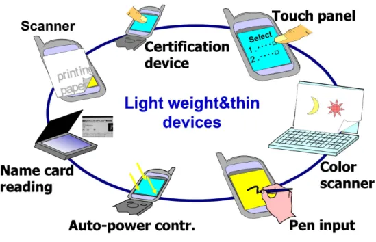
In addition to the ability to display color images, the integration of input display function that enables it to capture image in LTPS TFT-LCD technology is needed. The input display technology opens opportunities for new applications for personal and business use. The new technology is scalable up and down, and can be applied to diverse products, from cellular phones to personal computers.
The full scope to our imagination concerning future use of “Input Display” is shown in Fig. 1.8. Its wide range of usage will include recording of text or images for on-line shopping and the like with a scanner device saving personal data and images
~ 8 ~
to a computer, auto-power control with photo-sensor suitable for extremely low power cellular phone, name card reading system and scanner detected by the photo sensor or ambient light sensor, detecting the position of finger or pen for some touch-sensing, and so on.
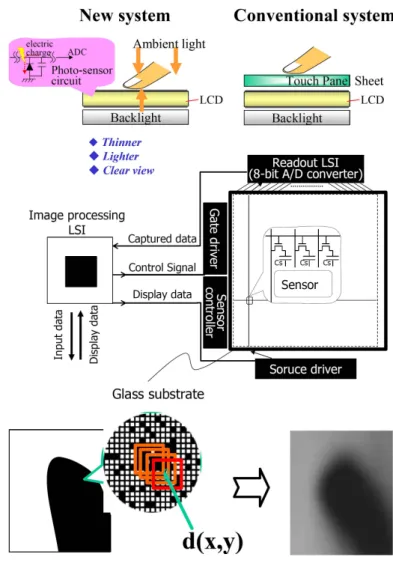
A technique of forming an optical sensor using LTPS TFT fabrication process is developed intended to incorporate these new functions in the display without an additional screen or behind the display. The input function is achieved through photo sensors embedded in each sub-pixel and the schematic principle of input display is shown in the top of Fig. 1.8. The light from the backlight goes through the cell, and then it was reflected by the surface of the object placed face down on the display, and captured by the photo sensors. The current through the sensor was modulated according to the reflectance of the object, which corresponded to the contrast of the captured image.
The bottom of Fig. 1.9 shows the array panel with three kinds of peripheral circuits; signal processor, display driver, and gate driver. The signal processor which is a data output circuit plays a role of capturing and processing the photo sensor signals, and then that is converted to a suitable form for display. The converted signals are then introduced to the display driver and the captured images are reappeared. This technique is applied to some products like card reading system illustrated in Fig. 1.9. Last, the gate driver controls both the pixel TFT and the sensor circuit. The sensor circuit integrations of LTPS enable to reduce the connecting pins (display and sensor terminals), which number almost double without circuit integration. Application to color image capturing has been realized by successively capturing through red, green, and blue (RGB) color filter, and then synthesizing their captured image.
~ 9 ~
Figure 1.8 Future applications of “Input Display”.
~ 10 ~
A novel touch panel system is shown in Fig. 1.10. The top of this figure shows the integration of touch panel function and digitizer function with no additional device on the display by forming a photo sensor in each sub-pixel. The illumination of ambient light is detected with some indispensable algorithms for the touch panel function and the grayscale image data suitable for finger touch location can be detected, as shown in the middle of Fig. 1.10.
Figure 1.10 The system architecture and image-capturing finger of the new touch panel.
~ 11 ~
And the configuration of display/sensor circuits with large scale integration (LSI) is presented simultaneously. The bottom of the figure shows illustration and captured grayscale bitmap image of a finger approaching to the LCD. The ADC is needed in periphery of the touch panel system to convert the sensing analog signals (illumination of the ambient light) to digital form to represent the grayscale level.
1.1.4 Thermal Influence on LCDs [8], [9], [10]
Optical characteristics of TFT-LCDs are significantly dependent on the panel temperature, hence the temperature characteristics are still an issue. For wide usage in thermally harsh environments, LCD should use a robust temperature compensation system to high reliability and to maintain performance.
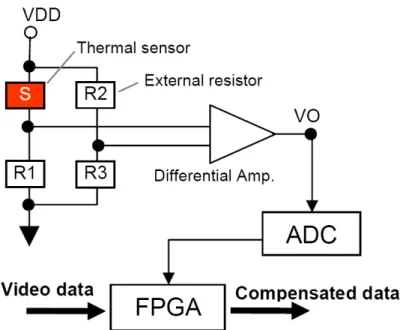
Fig. 1.11 and Fig. 1.12 show the thermal compensation architecture using a thermal sensor with a feedback control [8]. The metal film-type thermal sensors were integrated into the thermal crystal layer without any additional fabrication process steps. As shown in Fig. 1.12, the temperature readout circuit consists of an external full bridge circuit and a differential amplifier to minimize analog noise level. The analog sensor signal is converted to a digital signal by an ADC and then connected to FPGA system.
Figure 1.11 TAD (Thermally adaptive driving) integrated thermal sensor system architecture.
~ 12 ~
Figure 1.12 The temperature readout circuit consists of an external full bridge circuit and a differential amplifier.
1.1.5 Summary
According to above discussion, it can be seen that the integration of the input display function is developed and the fabrication cost will gradually be lowed and SOP will be implemented step by step in the future. Such integration technology contributes to shorten the product lead-time because lengthy development time of ICs can be eliminated. Actually, this integration level has been proceeding from simple digital circuits to the sophisticated ones. ADCs are widely used in interface of the analog sensing circuits and digital processing circuits such as the touch panel system or the thermal compensation system to convert the analog sensor signals into a digital signal and then processed by some digital circuits or FPGA as the above two sections demonstration. Thus, integration of ADC on the glass substrate is value-added.
In silicon CMOS technology, delta-sigma ADC has been widely used in VLSI industry. With the small amount of analog circuitry, the delta-sigma ADC is very
~ 13 ~
economically competitive with other types of data converters, such as pipeline ADC or flash ADC, for high resolution applications in the frequency range from kilohertz scale to hundred kilohertz scale. In this thesis, the circuit of delta-sigma ADC designed and realized in a 3-μm LTPS process is proposed.
1.2 Background Knowledge of Thin-Film Transistors Liquid Crystal
Displays
1.2.1 Brief Introduction of Liquid Crystal Displays [11], [12]
A liquid crystal display (LCD) is an electronically-modulated optical device shaped into a thin, flat panel made up of any number of color or monochrome pixels filled with liquid crystals and arrayed in front of a light source (backlight) or reflector.
The incident light can be modulated through the liquid crystal as shown in Fig. 1.13. There are two perpendicular polarizer filled with liquid crystal molecule. In general, the first polarizer of a couple of polarizers is called polarizer and the second polarizer of these is called analyzer. The light can be blocked by a couple of polarizers with 90° phase error, is shown in Fig. 1.13 (a). If we twist the liquid crystal molecule by applying the specific electric field across it, the light still can pass the polarizer. This is because the direction of liquid crystal molecules varies with electric field and it can guide the light along the long axis, shown in Fig. 1.13 (b).
~ 14 ~
Figure 1.13 (a) A couple of polarizers with 90° phase error. (b) A couple of polarizers with liquid crystals.
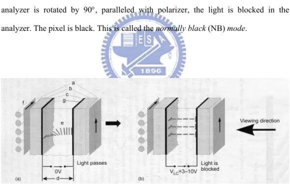
The twisted nematic (TN) device is the most common liquid crystal device and its structure is shown in Fig. 1.14. A structure of TN-LCD consists of a pair of polarizer to block the incident light, a pair of transparent electrode to modulate the liquid crystal molecule phase, and a pair of orientation layer which is also perpendicular to each other so the liquid crystal molecules arrange themselves in a helical structure, or twist.
The optical effect of a twisted nematic device in the voltage-on state is far less dependent on variations in the device thickness than that in the voltage-off state. Because of this, these devices are usually operated between crossed polarizers such that they appear bright with no voltage (the eye is much more sensitive to variations in the dark state than the bright state). These devices can also be operated between parallel polarizers, in which case the bright and dark states are reversed. The voltage-off dark state in this configuration appears blotchy, however, because of small variations of thickness across the device.
Fig. 1.14 (a) shows a pixel of a transmissive twisted nematic LC-cell with no voltage applied. The white backlight f passes the polarizer a. The light leaves it linearly polarized in the direction of the lines in the polarizer, and passes the glass substrate b, the transparent electrode c out of Indium-Tin-Oxide (ITO) and the
~ 15 ~
transparent orientation layer g. In this case, the analyzer is crossed with polarizer. The light can pass the analyzer without applied voltage due to the twisted nematic LC-cell and the pixel appears white. If the applied voltage is large enough as shown in Fig. 1.14 (b), the liquid crystal molecules in the center of the layer are almost completely untwisted and the polarization of the incident light is not rotated as it passes through the liquid crystal layer. This light will then be mainly polarized perpendicular to the second filter, and thus be blocked and the pixel will appear black. By controlling the voltage applied across the liquid crystal layer in each pixel, light can be allowed to pass through in varying amounts thus constituting different levels of gray.
This operation is termed the normally white (NW) mode. On the contrary, if the analyzer is rotated by 90°, paralleled with polarizer, the light is blocked in the analyzer. The pixel is black. This is called the normally black (NB) mode.
Figure 1.14 The structure of a TN-LCD (a) while light is passing, and (b) while light is blocked. a: polarizer; b: glass substrate; c: transparent electrode; g: orientation layer; e: liquid crystal; f: illumination.
~ 16 ~
1.2.2 Liquid Crystal Display Module Structure
The cross section structure of TFT-LCD panel is shown in Fig. 1.15 particularly. It can be roughly divided into two part, TFT array substrate and color filter substrate, by liquid crystal filled in the center of LCD panel. We still need a backlight module including an illuminator and a light guilder since liquid crystal molecule cannot light by itself. However it usually consumes the most power of the system, some applications such as mobile communications try to exclude or replace it from the system. There consists of a polarizer, a glass substrate, a transparent electrode and an orientation layer in TFT array substrate. In color filter substrate, it is composed of an orientation layer, a transparent electrode, color filters, a glass substrate and a polarizer. Most transparent electrodes are made by ITO, and they can control the directions of liquid crystal molecules in each pixel by voltage supplied from TFT on the glass substrate. Color filters contain three original colors, red, green, and blue (RGB). As the degree of light, named “gray level”, can be well controlled in each pixel covered by color filer, we will get more than million kinds of colors.
~ 17 ~
1.3 Thesis Organization
The fundamentals and realization of the delta-sigma modulator are discussed in chapter 2. The concept and simulation results of the decimation filter are discussed in chapter 3. Then, the delta-sigma ADC which is fabricated on the glass substrate in 3-μm LTPS process is measured and discussed in chapter 4. In the last chapter, the conclusions of this thesis and the future work are stated.
~ 18 ~
Chapter 2
Fundamentals and Realization of
First-order Delta-sigma Modulator
2.1 Introduction
2.1.1 Nyquist-rate and Oversampled Converter [18]
ADCs can be classified into two categories: Nyquist-rate and oversampled converter. In the former category, each input sample of ADCs is separately processed, that is, one output data is only dependent on one input sample. Nyquist-rate converter is a time-invariant and memory-less converter. Besides, the converter is one-to-one correspondence between the input and output samples. The sampling rate of the Nyquist-rate converter can be as low as Nyquist’s criterion requires that is twice as the input signal bandwidth. (Actually, the sampling rate is chosen higher than the minimum value for practical reason).
The linearity and accuracy of the Nyquist-rate converter is mostly determined by the matching accuracy of the analog components used in the implementation, such as resistors, current sources, capacitors, and so on. Practical conditions restrict the matching condition, and the effective number of bits (ENOB) is about 12 in the silicon process. Thus, the converter is hardly applied in high resolution applications. In order to overcome this issue, the oversampling converter has been investigated.
Oversampling converter is able to achieve over 20 ENOB resolution in the silicon process by using higher sampling rate. The sampling rate of the oversampling converter is higher than that of the Nyquist-rate by a factor between 8 and 512 typically. In addition, the oversampling converter incorporates memory element to utilize all preceding input values to generate each output. Its input/output relation is
~ 19 ~
not one-to-one correspondence anymore. The accuracy of the converter is evaluated by comparing the complete input and output waveform either in time domain or in frequency domain. Signal-to-noise ratio (SNR) calculation is a common method to analyze the accuracy for a sinusoidal wave input of the converter. Then, ENOB can be derived by equation (2.1).
1.76
6.02
SNR
ENOB
=
−
(2.1) The realization of the oversampling converters requires not only some analog stages but part of digital circuitry. Both analog and digital part of the oversampling converter needs operating faster than the Nyquist-rate converter. However, the accuracy requirements on the analog components are relaxed compared to those associated with Nyquist-rate converters. Besides, the extra cost paid for high accuracy is higher sampling rate and extra digital circuitry. As the digital IC technology advances, these costs are getting cheaper. Hence, the oversampling converter is taking the place of the Nyquist-rate converter in many applications.2.1.2 Fundamentals of the First-order Delta-sigma Modulator [16], [18]
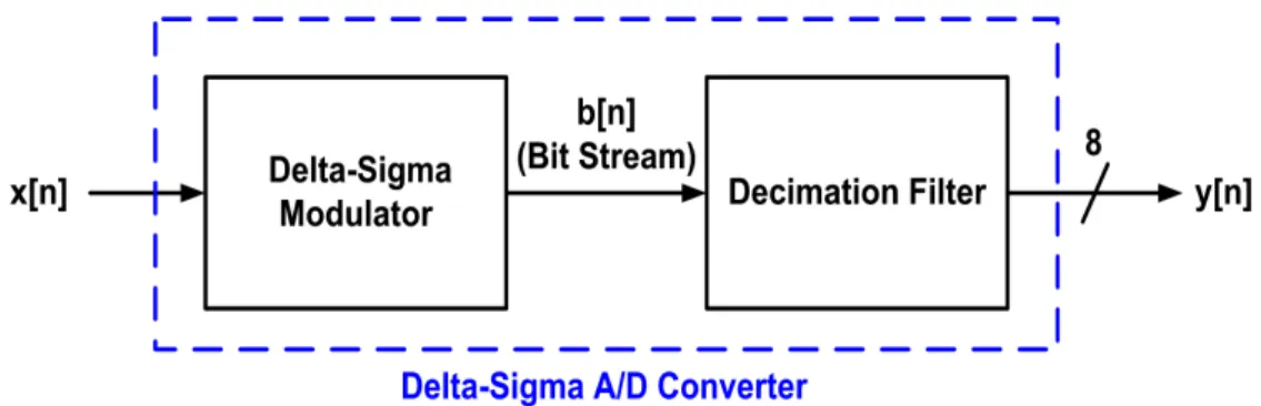
The oversampling ADC discussed here is the delta-sigma ADCs which consist of two basic blocks, a delta-sigma modulator and a decimation filter, as shown in Fig. 2.1. The delta-sigma modulator in the delta-sigma ADC is running continuously to transform input signal x[n] into a 1-bit bit stream b[n]. Then, the bit stream generated from the delta-sigma modulator will be processed by the decimation filter to remove the out-of-band noise and produce 8-bit digital output y[n].
The detail discussion of the delta-sigma modulator will be elaborated afterward in this chapter, and the decimation filter will be discussed in chapter 3.
~ 20 ~
Figure 2.1 Basic circuit diagram of Delta-sigma ADC consists of delta-sigma modulator and decimation filter.
Fig. 2.2 shows the block diagram of delta-sigma modulator. There is a feedback loop containing a loop filter and a low resolution ADC (here, an integrator and a quantizer) in the forward path of the loop. Besides, there is a DAC in the feedback path. The single bit digital output b[n] is converted into one of two analog levels by the single-bit feedback DAC. Furthermore, the output of the DAC is subtracted from the analog input signal in the summing amplifier. The resultant error signal from the summing amplifier output is low-pass filtered by the integrator and the integrated error signal polarity is detected by the quantizer. By observing that the differencing at the input followed by a summation in the loop filter, this structure is called a
delta-sigma modulator.
~ 21 ~
Analyzing Fig. 2.2, it can easily be shown that the output signal at time n is
[ ]
[
1] ( [ ]
[
1])
b n
=
x n
− +
e n
−
e n
−
. (2.2) The digital output contains a delay, but otherwise unchanged replica of the analog input signal x, and a differentiated term of the quantization noise error e. The differentiation term is suppressed if the frequency of the quantization noise e is much lower than the sampling rate. On the contrary, the two adjacent sampled data of the high frequency quantization noise data may not approach each other. Thus, the quantization noise contribute to the system is attenuated in low frequency but enhanced in high frequency. This kind of process is now called noise shaping [17].Observing the delta-sigma modulator in z-domain to complete the concept of that is elaborated. From Fig.2.2, the transfer function of the discrete time integrator can be derived as 1 1
( )
1
z
H z
z
− −=
−
. (2.3) Then, the input/output relation of the modulator is derived and given by1 1
( )
1
( )
( )
( )
1
( )
1
( )
( ) (1
) ( )
H z
B z
X z
E z
H z
H z
z X z
−z
−E z
=
+
+
+
=
+ −
. (2.4)The input signal simply goes straight through the delta-sigma modulator with only one delay is verified again by the illustration in the equation (2.4). Thus, z-1 is defined as signal transfer function (STF), and 1-z-1 is defined as noise transfer function (NTF). The magnitude of the NTF is derived in equation (2.5) where
Ω
is equal to2 f
π
overf
s. The magnitude of the NTF in low frequency is near 0 and the maximum value of the magnitude of the NTF occurs whence the frequency is half of the sampling frequency. Thus, NTF is a high pass function.~ 22 ~
2 2
2 1 2 2
1
1
j1 cos
sin
(2sin )
NTF
= −
z
−= −
e
Ω= −
Ω +
j
Ω =
Ω
(2.5)The high level quantization noise e generated by the quntizer, which is approximated as a white-noise source, is high pass shaped by the NTF. Thus, the in band noise is attenuated to reach a higher resolution architecture by a low resolution quantizer [15].
Any nonlinearity of the quantizer is simply combined with the quantization error
e and thus suppressed in-band along with e. However, nonlinear distortion in the DAC
affects the output signal without any shaping, and it represents a major limitation on the attainable performance. In order to solve this problem, single-bit quantizer is used. In such case, the input/output characteristic of the DAC consists of only two levels to ensure the inherent linear operation of DAC. However, using single-bit quantization means the output of the delta-sigma modulator contains only two level, either ‘logic-0’ or ‘logic-1’. How to translate the output signal into available message to realize what is the input signal becomes an important question.
By considering the delta-sigma modulator by the block diagram in Fig. 2.2, the relation between x[n], output bit stream b[n], and the output of the integrator v[n] in discrete time can be expressed as
[
1]
[ ]
[ ]
[ ]
v n
+ =
x n
−
b n
+
v n
. (2.6) Equation (2.6) can then be used to generate the sequences v[n] and b[n] from a given input x[n] with the initial condition of v[0]. The typical converting example, sequential operations of delta-sigma modulator with an input signal x[n] of 6V andv[0] of 1V, is listed in Table 2.1.
By observing table 1, b[n] is a periodic signal with its period of 5 cycles and there exists 3 cycles of ‘logic-1’ in one period. Thus, the probability of ‘logic-1’ in the bit stream is 0.6 (3/5), which is correctly equal to the input voltage ratio (x over 10V). As long as the input voltage x goes high, the probability of ‘logic-1’ of the output bit
~ 23 ~
stream of the delta-sigma modulator also goes high. Therefore, different probability of ‘logic-1’ of the output bit stream of the delta-sigma modulator may successfully tell different input x.
n 0 1 2 3 4 5 6
x[n] 6 6 6 6 6 6 6 v[n] 1 -3 3 -1 5 1 -3 b[n] 10 0 10 0 10 10 0
Table 2.1 The operation of delta-sigma modulator with an input signal x[n] of 6V.
2.2 Circuits Implementation on Glass Substrate
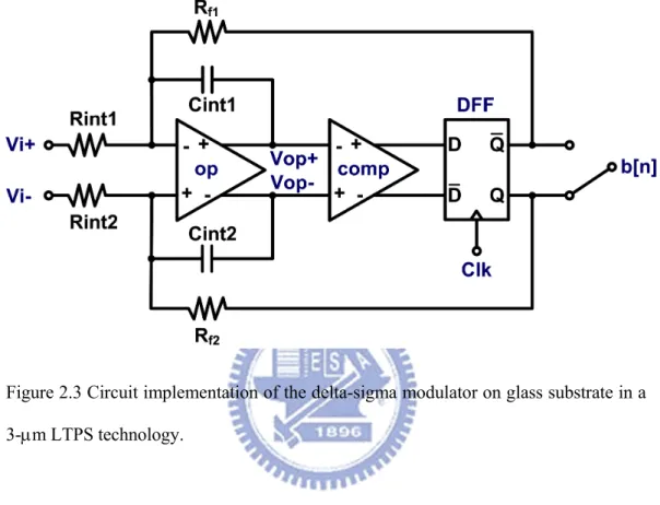
Fig. 2.3 shows a continuous-time realization of delta-sigma modulator using fully-differential architecture to overcome the common-mode noise generating by process variation. In this application, there exists a comparator followed by a D flip-flop while the DAC function performed by the Rf1 and Rf2 resistors connected the
D flip-flop outputs with the op-amp inputs. Here the positive input Vi+ is defined as x[n] shown in Fig. 2.2, and Vi- is equal to ten minus Vi+, under the operation voltage (Vdd) of 10 V.
As the output voltage of the D flip-flop b[n] is ‘logic-1’, it feeds back a positive charge through Rf2 and negative charge through Rf1. Then, it drives the output of the
integrator Vop- down and driving Vop+ up. As soon as the Vop+ is higher than Vop-,
b[n] is driving to ‘logic-0’, forming a negative feedback loop. Besides, when the
positive input voltage Vi+ is larger than half of the supply voltage (10V), the charge increment in capacitance Cint2 during high b[n] level in one clock cycle is less than charge decrement in capacitance Cint1 during low b[n] level. Thus, the large input
~ 24 ~
signal will produce high probability of ‘logic-1’ in the bit steam b[n]. This is proven again in the circuit level. The detailed circuit implementation will be discussed soon in the following section.
Figure 2.3 Circuit implementation of the delta-sigma modulator on glass substrate in a 3-μm LTPS technology.
2.2.1 Design of Fully-differential Folded-cascode Operational Amplifier
This section analyzes the frequency response of the fully differential folded-cascode amplifier. The schematic diagram of the fully-differential folded-cascode operational amplifier is shown in Fig. 2.4. Compared with the two stage operational amplifier, this architecture has better input common mode range and power supply rejection ratio. In particular, it provides large gain and it is easier to frequency compensate (the load capacitance is also the compensation capacitor). Furthermore, it does not suffer from frequency degradation of the power supply rejection ratio unlike the two stage operational amplifier. The p-channel M1 and M2
~ 25 ~
are the input driver transistors, M1A, M2A, M11 and M12 formed n-type cascode load
devices, and M3A, M4A, M3 and M4 formed p-type cascode load devices. One
important design point is that the dc current flowing through the cascode load (M3 and
M4) should be designed never going to zero. If the current goes to zero, a delay is
needed in turning these out of current transistors back on because of the parasitic capacitances that must be charged. To suppose the input differential voltage is large enough that transistor M1 turns off and M2 turns on, all of I3 flows through M2,
resulting in I2=I3. If I5 is not greater than I3, then the current I4 will be zero. Thus, the value of I5 is normally between I3 and twice of I3 to avoid this delay problem.
The common-mode feedback (CMFB) circuit is needed for any fully-differential operational amplifiers. Without it the common-mode output remains undefined, and the amplifier will drift out of the high gain operating regime. The CMFB can be achieved by controlling the bias voltages of M11 and M12. The CMFB circuit
comprises of transistors MCM1– MCM6, where the differential currents of two
differential pairs (MCM1, MCM2 and MCM3, MCM4) flow into a current-mirror load MCM5,
MCM6. The common-mode voltage is held at the reference potential VCM, which is
usually analog ground in order to maximize output signal swing.
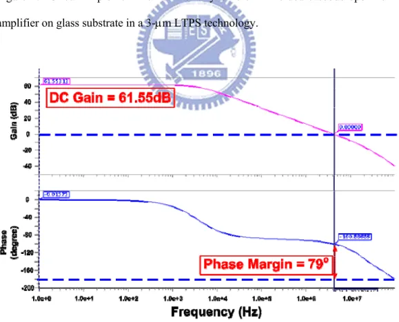
Finally, the amplifier is simulated using eldo simulator. The simulated frequency response of the fully differential operational amplifier in open-loop condition is shown in Fig. 2.5. The characteristic of the operational amplifier, such as the DC gain and the phase margin are found to be 61.55 dB and 79o, respectively. The approximate gain bandwidth is found to be 4.3MHz, and the average power dissipation is about 2.3 mWatt.
~ 26 ~
Figure 2.4 Circuit implementation of the fully-differential folded-cascode operational amplifier on glass substrate in a 3-μm LTPS technology.
Figure 2.5 The simulated frequency response of the fully differential operational amplifier in open-loop condition.
~ 27 ~
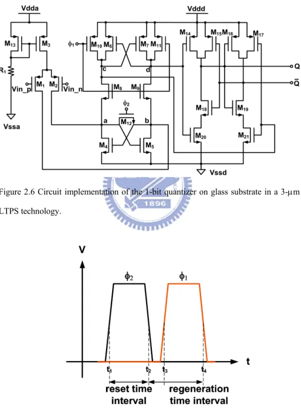
2.2.2 Design of 1-bit Quantizer
This section presents the design of the 1-bit quantizer appropriate for use in conventional and delta-sigma converters. The schematic diagram of the quantizer is depicted in Fig. 2.6. It comprises of three parts as following. The first part is the differential input pair, M1 and M2. The second part is a latch circuit composed of a
n-type flip-flop, M4 and M5, with a pair of n-type transfer gate, M8 and M9. There are
also a p-type flip-flop, M6 and M7, with a pair of p-type precharge transistors, M10 and
M11, and the transistor M12 is a switch for resetting. The third part is a latch composed
of transistor M14-M21.
φ1 and φ2 are the two non-overlapping clocks as depicted in Fig. 2.7. The
dynamic operation of this circuit can be divided into two intervals, reset time interval and regeneration time interval, respectively. During φ2, the comparator is in reset
mode and transistors M8 and M9 isolate the p-type flip-flop from the n-type flip-flop.
After the input stage settles on its decision, a voltage which is proportional to the input voltage difference is established between node a and node b. Node c and node d are precharged to the power supply voltage by two closed transistor, M10 and M11.
Transistors M20 and M21 are closed and transistors M14 and M15 are open, then two
inverters are formed with transistors M16-M19. The output signal Q is injected into one
inverter producing its complement which is injected into another inverter simultaneously. Thus, the output Q is forced to keep the previous state value by the followed SR latch. Any change in the input stage will not affect the output when the circuit is in the reset time interval.
The regeneration mode is initialized when transistor M12 is opening. The n-type
flip-flop, together with the p-type flip-flop, regenerates the voltage differences between nodes a and b and between nodes c and d. Then, the voltage difference between node c and d is amplified to near the power supply voltage. The following
~ 28 ~
SR latch is driven to full complementary digital output levels at the end of the regeneration mode. Thus, the polarity of the 1-bit quantizer is decided in the regeneration time interval and kept in the reset time interval.
Figure 2.6 Circuit implementation of the 1-bit quantizer on glass substrate in a 3-μm LTPS technology.
~ 29 ~
Finally, the simulated result of the quantizer is shown in Fig. 2.8. It can successfully find out which of the two input nodes is higher and the result is shown in the output.
Figure 2.8 The simulated result of the 1-bit quantizer.
2.2.3 Design of D Flip-flop
The schematic diagram of the D flip-flop is shown in Fig. 2.9. This flip-flop requires only one clock, called a true-single-phase-clock (TSPC) flip-flop. As the input signal D is low, transistor M5 is closed as the clock signal (Clk) is low. Then the
drain of transistor M5 is pulled to low and so is the output signal Q. Similarly, the
output signal Q will be high as long as the input signal D is high in the Clk signal is in its rising edge. The simulated result of the D flip-flop is shown in Fig. 2.10.
~ 30 ~
Figure 2.9 Circuit implementation of the D flip-flop on glass substrate in a 3-μm LTPS technology.
~ 31 ~
2.2.4 Summary
A first-order delta-sigma modulator is implemented by combining the operational amplifier, 1-bit quantizer, and the D flip-flop discussed above. The simulated results are shown in the following pictures, Fig. 2.11 – Fig. 2.14, with different input data.
By the section 2.2.1 and the foreword of section 2.2, the probability of ‘logic-1’ in the output bit stream of the delta-sigma modulator will be correctly equal to the input voltage ratio, x over the power supply voltage, where the variable x is the input signal used and shown in Fig 2.2. However, in this fully differential architecture of the delta-sigma modulator, the input voltage ratio should be modified into equation (2.7) as shown below.
(
) (
)
Vi
Vi
Vi
+
+ +
−
(2.7) Thus, different input voltage should produce different probability of ‘logic-1’ at the output of the modulator. As the input voltage Vi+ is 8V, the probability of ‘logic-1’ should be 0.8 calculated by equation (2.7).In the mean time, the simulated results using the eldo simulator are shown in Fig. 2.11. The probability of ‘logic-1’ in one period is also calculated and listed in table 2.2, and which is equal to 0.808. That is, this circuit has worked successfully in this input situation. Next, different input situations have necessarily to be verified. Fig. 2.12 to Fig. 2.14 show that the simulated results of input signal Vi+ is 7V, 5V, and 3V, respectively. The probability of ‘logic-1’ in one period of these different three situations is calculated and tabled in table 2.3 to table 2.5 simultaneously. As the input signal Vi+ is 7V, the calculated probability result is 0.703. The input signal Vi+ are 5V and 3V, the calculated probability results are 0.5 and 0.293, respectively. By such calculation and simulation, this circuit is successfully verified by eldo simulator.
~ 32 ~
Figure 2.11 The simulated result of the first-order delta-sigma modulator when the input Vi+ is 8V.
Cycle number of ‘logic-1’ in one period 207 cycles
Period 256 cycles
Probability of ‘logic-1’ in one period 0.808
Table 2.2 The probability of ‘logic-1’ in one period is calculated and listed as Vi+ is 8V.
~ 33 ~
Figure 2.12 The simulated result of the first-order delta-sigma modulator when the input Vi+ is 7V.
Cycle number of ‘logic-1’ in one period 180 cycles
Period 256 cycles
Probability of ‘logic-1’ in one period 0.703
Table 2.3 The probability of ‘logic-1’ in one period is calculated and listed as Vi+ is 7V.
~ 34 ~
Figure 2.13 The simulated result of the first-order delta-sigma modulator when the input Vi+ is 5V.
Cycle number of ‘logic-1’ in one period 128 cycles
Period 256 cycles
Probability of ‘logic-1’ in one period 0.5
Table 2.4 The probability of ‘logic-1’ in one period is calculated and listed as Vi+ is 5V.
~ 35 ~
Figure 2.14 The simulated result of the first-order delta-sigma modulator when the input Vi+ is 3V.
Cycle number of ‘logic-1’ in one period 75 cycles
Period 256 cycles
Probability of ‘logic-1’ in one period 0.293
Table 2.5 The probability of ‘logic-1’ in one period is calculated and listed as Vi+ is 3V.
~ 36 ~
Chapter 3
Decimation Filter for First-order
Delta-sigma Modulator
3.1 Introduction
For a delta-sigma ADC, the delta-sigma modulator is operated with oversampling to produce 1-bit output stream in high data rate. However, the results of the modulator can’t represent the converting results of input analog signal directly. A decimation filter is thus needed to solve this problem. Decimation filter acts as a low-pass function to filter the signal outer the frequency band and decimate the output bit stream down to the Nyquist rate. This process changes the high sampling rate and low resolution digital signals into the high resolution digital signals. Then, the bit stream will be converted into 8-bit determined digital signals. In such case, a counter which is a finite-impulse-response (FIR) filter is used as a decimation filter to compute a running average of the output bit stream b[n] from the delta-sigma modulator and produce the 8-bit digital output. As the Fig. 3.1 shows, the input bit stream b[n] comes from the delta-sigma modulator discussed in chapter 2. Then, the decimation filter produces 8-bit output signal y[n]. The relation between bit stream
b[n] and 8-bit digital signal y[n] and how a counter could be seen as a decimation
filter are both discussed in the next section.
~ 37 ~
In such design, a counter is used to calculate the running average of the bit stream b[n] coming from the delta-sigma modulator and translate this message into the 8-bit digital code [18]. Thus, the output y[n] of the decimation filter can be expressed as a function of the bit stream b[n]. N numbers of successive data of b[n] are summed up and then divided by N as shown in equation (3.1).
1 0
1
[ ]
N[
]
iy n
b n i
N
− ==
∑
−
(3.1) Then, the z-domain transfer function of equation (3.1) can be derived as equation (3.2). The variable H1 is used to represent the system of the decimation filter. Thefrequency response of this system can also be derived by substituting the variable z in equation (3.1) for the exponential equation with the index number is j2πf as expressed
in equation (3.3). By observing this equation, this transfer function is composed by a sinc function divided by another one and why this circuit is termed as a Sinc filter can be figured out. 1 1
1 1
( )
1
Nz
H z
N
z
− −−
=
−
(3.2) 2 1(
)
(
)
( )
j fsinc Nf
H e
sinc f
π=
(3.3)By equation (3.3) derived above, the amplitude of the transfer function can be analyzed in different frequency. It is close to 1 near zero frequency and it decays as frequency increases in the mean while. It represents a low-pass filter. However, the harmonic tones of that transfer function in equation (3.3) exist in high frequency. These unexpected tones will contribute some noise to the delta-sigma ADC and cause this filter a non-ideal low-pass filter. Because of such problem, the noise in the output bit stream b[n] can be attenuated perfectly at only the certain frequencies. However, this filter used for the first-order delta-sigma modulator is adequate and very
~ 38 ~
economic. Thus, a non-ideal low-pass filter is applied by using a counter to be the decimation filter. Besides, more calculating number would lead to the error decrease gradually, even though the counter results in some error.
3.2 Circuits Implementation on Glass Substrate
The block diagram of the decimation filter is shown in Fig. 3.2. It consists of a counter, a register, and a divider. At the beginning of a new conversion, the counter and the register are both reset. The input signal b[n] is coming from the front circuit (delta-sigma modulator) and injecting into the counter. The counter will count up as long as the b[n] is ‘logic-1’ when the clock (Clk) is in the rising edge. Fig. 3.3 shows its timing chart. Once in every N clock cycles, the output of the counter is clocked into a register. In the mean time, the divider will produce the Clk_N signal to reset the counter. Thus, the output y[n] is down-sampled and represented in digital code. The counter produces k-bit output if N=2k, which may be interpreted as a binary fraction between 0 and 1. In this case, N is chosen as 256 for 8-bit digital output.
Next, the circuit implementation of the three parts of the decimation filter, the counter, the register, and the divider is discussed in the following section.
Figure 3.2 Block diagram of decimation filter composed of a counter, register, and a divider.
~ 39 ~
Figure 3.3 The timing chart represents the relation between the Clk, Clk_N, and the output signal y of the decimation filter.
3.2.1 Design of the Counter
At first, the design of the counter is demonstrated. However, the JK flip-flop needs to be discussed before how to design the counter. The JK flip-flop is the most widely used flip-flop because of its versatility and its block diagram is shown in Fig. 3.4.
Figure 3.4 The circuit implementation of the JK Flip-flop which comprises of some logic gates and two SR_latches.
~ 40 ~
The JK flip-flop consists of four AND gates, one inverter, and two SR_latches. It is obviously a master/slave structure. As the Clk signal is high, the front part of the JK flip-flop is on. If the input signals J and K are both high, the front SR_latch is controlled only by the signal which is feeding back from the output. If the output signal of the JK flip-flop, Q, is high, the input signal of the front SR_latch (S, R) is (0, 1). Hence, it drives the output of the front SR_latch (Q, Qb) becoming (0, 1). Then, as the Clk signal goes low, the output signal of the rear SR, Q, which is also the output signal of the JK flip-flop, is driving low. Thus, it is transformed into its complement. Another example is given as J and K are both low. In such case, the input signal of the front SR_latch (S, R) are both low no matter what the output signal fed back is. Thus, the output signal of the front latch will keep the value equal to its previous state. Similarly, as the Clk signal goes low, the signal coming from the front part will influence the rear part of the JK flip-flop. Then, its output signal is contained as its previous state. Besides, this JK flip-flop is obviously a negative edge trigger structure by the above deriving, and the Clr signal is used to reset this circuit. The discussion above is also demonstrated as the truth table in the table 3.1, and that two cases are mainly used in this application.
J K Q(t+1)
0 0 Q(t)
0 1 0 1 0 1
1 1 Q(t)
~ 41 ~
The block diagram of the counter is shown in Fig. 3.5. The counter contains 8 JK flip-flops whose input signal J and K are combined together. As the input J and K are both high, the output Q of that JK flip-flop will toggle. On the contrary, if J and K are both low, the output Q of that JK flip-flop will keep the previous state value. As the Fig. 3.5 shows, the input of the LSB JK flip-flop is b[n] produced by the delta-sigma modulator, and it is negative edge triggered by the Clk signal. The inputs of the other 7 JK flip-flops are all ‘1’ driven by the power supply voltage, and all of them are negative edge triggered by the previous stage output. Then, the output of the counter, c0-c7, are produced and also shown in Fig. 3.5.
Fig. 3.6 shows the timing chart of this counter as b[n] is high and the initial value of c0, c1, and c2 are all low (where this only least 3 significant bits are shown). As long
as the Clk is going to low, c0 is toggled. Similarly, every time when c0 is going to low,
c1 is toggled. The like c2-c7 will be produced similarly. Observing this operation
shown in Fig. 3.6, it can be found that the output of the counter is counted up and represented as 8-bit digital code.
Figure 3.5 The block diagram of the counter built up with the JK Flip-flop and controlled by the Clk and Clr signals where the input signal is b[n] and the output signal is c0-c7.
~ 42 ~
Figure 3.6 The timing chart of the counter as b[n] is high where the only least 3 significant bits are shown.
Otherwise, as long as b[n] is low, the least significant JK flip-flop will keep its output data c0. That is no negative edge will be found in c0, and all other outputs are
the same. Thus, the 8-bit digital output will be kept as b[n] is low and counted up as
b[n] is high in 256 cycles. Its output will be kept in the 8-bit register which is
illustrated in section 3.2.2 and then the counter will be reset and controlled by the divider circuit discussed in section 3.2.3.
3.2.2 Design of the Register
The register is used to keep the value calculated by the counter and the counter is just able to calculate next 256 data in the next time. Fig. 3.7 shows the block diagram of the register which consists of 8 D flip-flops, and the register is positive edge triggered by the Clk_N signal which is produced by the divider and will be discussed in the next section.
~ 43 ~
Figure 3.7 The block diagram of the register which consists of 8 D flip-flops which is positive edge triggered by the Clk signal.
3.2.3 Design of the Divider
The block diagram of the divider is shown in Fig. 3.8. The divider uses 8 D flip-flops as an inherent counter. The least significant D flip-flop is positive edge triggered by Clk and then reflects the input on the output. However, the input signals of all of the flip-flops are fed back by their own output, and specially is the complementary one (Qb). Thus, every time the Clk is going to high, q0 which is the
least significant bit of this counter is toggled. At the same time, q0 is also the signal
used to trigger the next D flip-flop, and q1 will toggle as long as q0 is going to high.
This operation is just like the counter discussed above; however, the counter here is a down-counter on the contrary and the output q0-q7 is counted down from 255 to 0
~ 44 ~
q4, q5, q6, and q7 have the same waveform; therefore, all of them are shown together.
As long as the counter here is counted to 0, the divider will produce a pulse in the output Clk_N by these 7 logic gates. Clk_N is used to reset the counter shown in section 3.2.1 and to trigger the 8-bit register.