i
國
立
交
通
大
學
電子工程學系 電子研究所
碩 士 論 文
人體通道通訊系統平台之設計
Design of Body Channel Communication
Emulation Platform
研 究 生: 林恕平
指導教授: 李鎮宜 教授
ii
人體通道通訊系統平台之設計
Design of Body Channel Communication
Emulation Platform
研 究 生: 林恕平
Student: Shu-Ping Lin
指導教授: 李鎮宜 教授
Advisor: Prof. Chen-Yi Lee
國 立 交 通 大 學
電子工程學系 電子研究所
碩 士 論 文
A Thesis
Submitted to Department of Electronics Engineering and Institute of Electronics
College of Electrical and Computer Engineering National Chiao Tung University
in partial Fulfillment of the Requirements for the Degree of
Master in
Electronics Engineering
October 2012
Hsinchu, Taiwan, Republic of China
iii
人體通道通訊系統平台之設計
學生:林恕平 指導教授:李鎮宜 博士
國立交通大學
電子工程學系 電子研究所
摘要
人體通道通訊是一項利用人體表面皮膚傳輸訊號之科技。其具有
高導通性、低傳輸頻率,以及限制訊號之傳輸於人體周遭等特性。這
些特性使人體通道通訊特別適合用於多媒體影音下載、行動健康看護
系統,以及門禁控制和結帳系統等應用。
為了達到低能耗之高速率傳輸、小面積,以及提供使用者舒適之
佩戴,本論文設計之人體通道通訊系統使用正交分頻多工傳輸策略以
及無石英震盪器。因無石英震盪器之頻率誤差較大,亦設計對應之頻
率校正方法。
本論文呈現一使用正交分頻多工傳輸策略以及無石英震盪器之
人體通道通訊系統平台。系統平台包含傳送端前端電路、接收端前端
電路,以及基頻收發器。系統平台目前可以達到 6.7Mbps 之穩定高速
傳輸。
iv
Design of Body Channel Communication
Emulation Platform
Student: Shu-Ping Lin Advisor: Dr. Chen-Yi Lee
Department of electronics engineering and Institute of electronics,
National Chiao Tung University
Abstract
Body channel communication (BCC) is an emerging technology
which uses skin of human body as transmission channel. It has
advantages such as high conductivity, low transmission frequency, and
the confinement of transmission signal to the body area. With those
advantages, BCC is very suitable for applications such as multimedia
downloading, access control and payment, and mobile health-care, and so
forth.
In order to get high data rate with low operation energy, as well as to
achieve small area and comfortable wearing, dedicated OFDM
transmission strategy, and on-chip oscillator (crystal-less) are introduced
to the BCC system. Due to frequency offset of on-chip oscillator, the
calibration methodology for crystal-less OFDM is included in the design.
This thesis presents a BCC emulation platform with dedicated
OFDM transmission strategy and on-chip oscillator features. The
emulation platform includes transmitter front-end, receiver front-end and
transceiver baseband. It can achieve reliable transmission with 6.7Mbps
data rate.
v
誌謝
在 Si2 實驗室的時間,是恕平在交大成長最快的一段時間。首先要感謝指導 教授-李鎮宜博士,給予恕平在研究方向、方法以及態度的指導。李老師所建構 出完善的研究環境以及強大研究團隊,讓恕平能夠在最好的環境跟最棒的團隊學 習成長。除了在研究方面的指導外,李老師也時常鼓勵我們要養成運動的習慣。 有健康的身體,做起事來效率才高。李老師做人做事的態度方法是我學習的榜樣。 另外也要感謝口試委員黃威教授、莊景德教授以及周世傑教授,你們能撥空來指 導並且給予我研究方面的建議,使得本篇論文可以更加完整。 特別感謝從專題時期就跟隨的偉豪學長。您在專業上的素養以及嚴謹的邏輯 思考等,讓恕平十分佩服。四年多下來,恕平從您身上學到非常多的東西,受益 良多。也感謝瑞元、燦文、盈杰、建螢、書餘以及秉原學長們,時常撥空給予我 研究上的建議。感謝曉涵學姊以及子均學長在我專題時期,給予我的協助。感謝 Si2 的研究團隊們,你們的幫忙及鼓勵,是恕平突破及成長的動力。 感謝 Si2 的夥伴博堯,從比利時以來的陪伴。我們一同旅遊運動健身跑步, 紓解研究上的壓力。感謝紝炘,在研究上的幫忙。讓我們一同合作,一起成長。 感謝佩妤、姿儀、方如、英秀以及鈺筠,你們讓 Si2 的研究氣氛更為和樂融洽。 最後感謝我的家人,因為你們的支持讓我可以順利的完成學位。vi
Table of Contents
Pages
Chapter 1: Introduction ... 1
1-1 Introduction to BCC ... 1
1-2 Motivation and Design Approach ... 4
1-3 Organization ... 5
Chapter 2: Overview of BCC and Crystal-less Integration ... 6
2-1 Body Channel Characteristics ... 6
2-1.1 Transfer Type ... 6
2-1.2 Types of Transmission ... 7
2-1.3 Path-loss ... 8
2-1.4 Body Antenna Effect ... 10
2-1.5 Body Channel Model ... 11
2-2 Crystal-less Integration Issues ... 17
2-2.1 Crystal-less Integration Overview ... 17
2-2.2 Carrier Frequency Offset ... 18
2-2.3 Sampling Clock Offset ... 19
Chapter 3: Design of Crystal-less OFDM-based Transceiver Baseband ... 21
3-1 OFDM Transmission Strategy ... 21
3-2 OFDM Packet Format ... 23
3-3 Proposed Crystal-less OFDM-based Transceiver Baseband ... 24
3-3.1 Baseband Overview ... 24
3-3.2 Synchronization and Clock Calibration ... 25
3-3.3 Channel Equalization ... 34
vii
3-4 Simulation Result ... 38
Chapter 4: Implementation of Transceiver ... 39
4-1 Transmitter Front-end ... 41
4-2 Receiver Front-end... 44
4-3 Emulation of Clock Drift Calibration ... 49
4-4 Emulation of AGC ... 52
Chapter 5: Experiment Result ... 53
5-1 Measurement Result... 53
5-2 Comparison Result ... 58
Chapter 6: Conclusion and Future Work ... 59
6-1 Conclusion ... 59
6-2 Future Work ... 60
viii
List of Figures
Pages
Fig. 1-1 Multimedia download ... 2
Fig. 1-2 Mobile health-care application ... 3
Fig. 1-3 Access control and payment ... 4
Fig. 2-1 BCC Coupling types ... 6
Fig. 2-2 BCC transmission types ... 7
Fig. 2-3 Measurement set-up ... 8
Fig. 2-4 Frequency response ... 9
Fig. 2-5 Interference measurement ... 11
Fig. 2-6 Body area network scenario ... 12
Fig. 2-7 Channel model ... 13
Fig. 2-8 Frequency response ... 13
Fig. 2-9 Noise characteristic ... 14
Fig. 2-10 Channel model block diagram ... 14
Fig. 2-11 Channel with dair = dbody = 10cm... 16
Fig. 2-12 Channel with dair = dbody = 30cm... 16
Fig. 2-13 Channel with dair =100cm, dbody = 150cm ... 17
Fig. 2-14 On-chip oscillator integration ... 18
Fig. 2-15 CFO and SCO effect ... 18
Fig. 3-1 OFDM transmission strategy ... 22
Fig. 3-2 Packet Format ... 23
Fig. 3-3 Short Preamble ... 23
Fig. 3-4 Long Preamble ... 24
ix
Fig. 3-6 Auto-correlation Waveform ... 26
Fig. 3-7 AGC Flow Chart ... 27
Fig. 3-8 Clock Drift Estimator ... 28
Fig. 3-9 Matlab simulation of clock drift estimation ... 29
Fig. 3-10 Phase Ⅱ Estimator ... 30
Fig. 3-11 Generation of detector coefficient... 31
Fig. 3-12 Clock calibration example ... 31
Fig. 3-13 Conventional cross-correlation ... 32
Fig. 3-14 Multipath effect ... 33
Fig. 3-15 Dual correlation waveform ... 34
Fig. 3-16 Frequency response ... 35
Fig. 3-17 Phase distortion in frequency domain ... 36
Fig. 3-18 Matlab simulation model ... 38
Fig. 3-19 Matlab simulation result with different clock offsets ... 38
Fig. 4-1 Transceiver block diagram ... 39
Fig. 4-2 Emulation platform picture ... 40
Fig. 4-3 Transmitter front-end picture ... 41
Fig. 4-4 Impedance frequency response ... 42
Fig. 4-5 Power planning ... 43
Fig. 4-6 Receiver front-end picture ... 44
Fig. 4-7 Direct conversion receiver ... 45
Fig. 4-8 IQ gain mismatch ... 47
Fig. 4-9 I and Q channel attenuator ... 47
Fig. 4-10 Coupling interference... 48
x
Fig. 4-12 Clock calibration emulation flow ... 49
Fig. 4-13 DDFS ouput (a)Before calibration, (b)After calibration... 50
Fig. 4-14 Short preamble waveform(a) Before calibration, (b)After calibration .... 51
Fig. 4-15 AGC emulation flow ... 52
Fig. 4-16 Emulation result ... 52
Fig. 5-1 DAC output ... 54
Fig. 5-2 MOD output ... 54
Fig. 5-3 ADC output ... 55
Fig. 5-4 Received baseband signal ... 55
xi
List of Tables
Pages
Table 2-1 Path-loss measurement... 9
Table 2-2 Body area network scenario ... 12
Table 4-1 Transmitter front-end components ... 41
Table 4-2 Receiver front-end components ... 44
1
Chapter 1:
Introduction
1-1
Introduction to BCC
Body channel communication (BCC) is an emerging technology which uses skin of human body as transmission channel. There are several advantages of body channel. First, Human body has high conductivity compared with air. Second, the transmission frequency of BCC is relatively low compared to other wireless communication. This removes the need for large antenna, and thus reduces the power consumption of system. Moreover, the transmission of signal is confined to the body area. These advantages make BCC suitable for following application scenario.
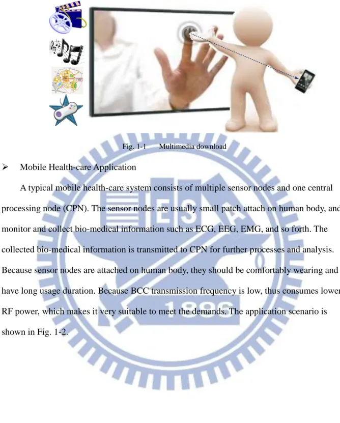
Multimedia Download
Digital signage is getting more and more popular. However, how to take away information from digital signage still remains a hot issue. Existing communication technology such as Bluetooth and WiFi has high speed data-rate. However, users have to go through miscellaneous steps in order to download information. If we use BCC, when user touches digital signage, the channel between digital signage and mobile device is connected by body channel, and the information can be downloaded to the mobile devices. To download information within seconds, data rate is an important issue. The application scenario is shown in Fig. 1-1.
2
Fig. 1-1 Multimedia download
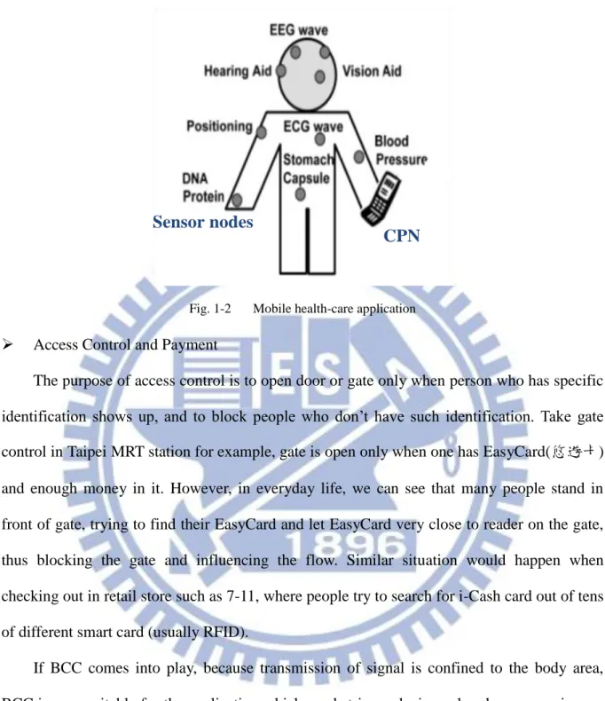
Mobile Health-care Application
A typical mobile health-care system consists of multiple sensor nodes and one central processing node (CPN). The sensor nodes are usually small patch attach on human body, and monitor and collect bio-medical information such as ECG, EEG, EMG, and so forth. The collected bio-medical information is transmitted to CPN for further processes and analysis. Because sensor nodes are attached on human body, they should be comfortably wearing and have long usage duration. Because BCC transmission frequency is low, thus consumes lower RF power, which makes it very suitable to meet the demands. The application scenario is shown in Fig. 1-2.
3
Sensor nodes
CPN
Fig. 1-2 Mobile health-care application
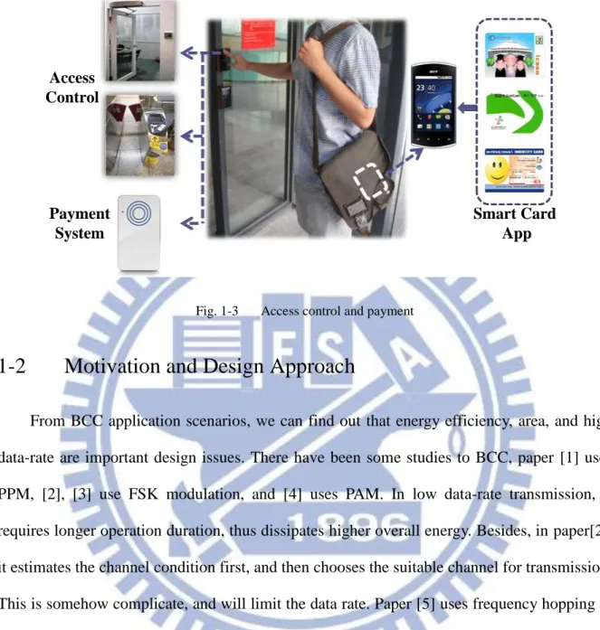
Access Control and Payment
The purpose of access control is to open door or gate only when person who has specific identification shows up, and to block people who don’t have such identification. Take gate control in Taipei MRT station for example, gate is open only when one has EasyCard(悠遊卡) and enough money in it. However, in everyday life, we can see that many people stand in front of gate, trying to find their EasyCard and let EasyCard very close to reader on the gate, thus blocking the gate and influencing the flow. Similar situation would happen when checking out in retail store such as 7-11, where people try to search for i-Cash card out of tens of different smart card (usually RFID).
If BCC comes into play, because transmission of signal is confined to the body area, BCC is very suitable for the application which needs trigger device only when person is near to that device, such as access control and payment application shown before. The application scenario is shown in Fig. 1-3, we turn the RFID smart cards (EasyCard, i-Cash...) into App in mobile devices, such as smart phone and tablet. When user touches reader, BCC then connect reader and mobile devices. Mobile devices could be in packet, backpack, where it is near body area.
4 Smart Card App Access Control Payment System
Fig. 1-3 Access control and payment
1-2
Motivation and Design Approach
From BCC application scenarios, we can find out that energy efficiency, area, and high data-rate are important design issues. There have been some studies to BCC, paper [1] uses PPM, [2], [3] use FSK modulation, and [4] uses PAM. In low data-rate transmission, it requires longer operation duration, thus dissipates higher overall energy. Besides, in paper[2], it estimates the channel condition first, and then chooses the suitable channel for transmission. This is somehow complicate, and will limit the data rate. Paper [5] uses frequency hopping to combat the channel effect. However, it occupies pretty large bandwidth (80MHz). When it comes to issue of area and comfort of wearing, papers[2], [4] and [5] use external clock source. The external clock source usually is quartz crystal, which is large and bulky.
This thesis proposes a crystal-less OFDM system for BCC applications. With dedicated OFDM transmission strategy, high data rate and energy efficiency is achieved. For comfortable wearing, we use on-chip oscillator integration (crystal-less) to replace large and bulky quartz crystal. On-chip oscillator has supreme excess compared with quartz crystal
5
oscillator in terms of area and process integration[6]. However, the frequency offset of the on-chip oscillator is larger than the tolerance of conventional packet-based OFDM system, thus a dedicated clock calibration methodology is included in the system.
1-3
Organization
The thesis is organized as follows. Chapter 2 is the overview of the proposed system, which describes body channel characteristics and crystal-less issues. The design of proposed BCC transceiver is shown in Chapter 3. The BCC emulation platform implementation is shown in Chapter 4. The experiment result is sown in Chapter 5. Finally, Chapter 6 gives the conclusion and future work.
6
Chapter 2:
Overview of BCC and
Crystal-less Integration
2-1
Body Channel Characteristics
2-1.1
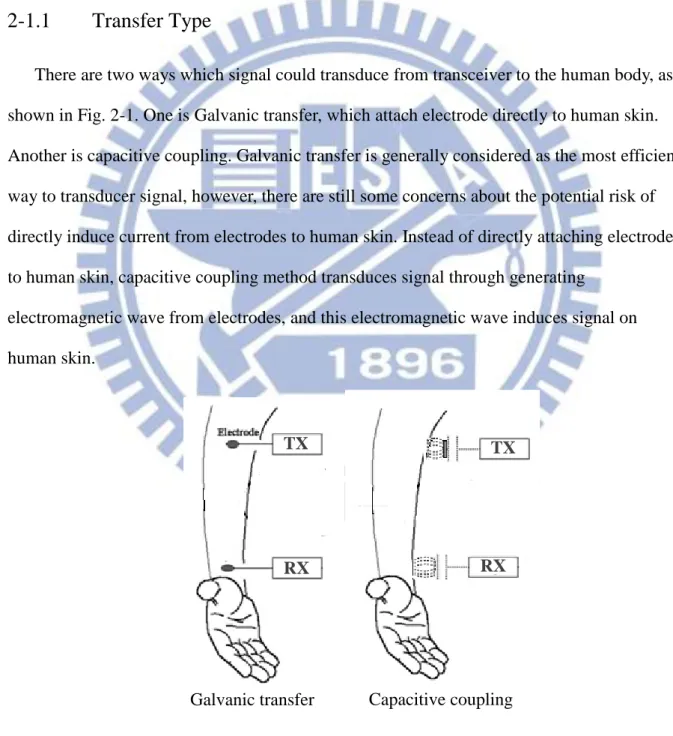
Transfer Type
There are two ways which signal could transduce from transceiver to the human body, as shown in Fig. 2-1. One is Galvanic transfer, which attach electrode directly to human skin. Another is capacitive coupling. Galvanic transfer is generally considered as the most efficient way to transducer signal, however, there are still some concerns about the potential risk of directly induce current from electrodes to human skin. Instead of directly attaching electrodes to human skin, capacitive coupling method transduces signal through generating
electromagnetic wave from electrodes, and this electromagnetic wave induces signal on human skin.
TX TX
RX RX
Galvanic transfer Capacitive coupling Fig. 2-1 BCC Coupling types
7
2-1.2
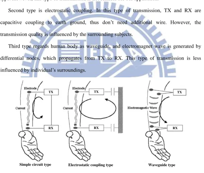
Types of Transmission
There are three types of transmission for BCC [7], as shown in Fig. 2-2, which are simple circuit type, electrostatic coupling type, and waveguide type.
The simple circuit type treats human body simply as conductor. Although it is a simple transmission method, it needs additional wire to connect TX and RX. Fat meter belong to this type. However, this type of transmission is not suitable for our application.
Second type is electrostatic coupling. In this type of transmission, TX and RX are capacitive coupling to earth ground, thus don’t need additional wire. However, the transmission quality is influenced by the surrounding subjects.
Third type regards human body as waveguide, and electromagnet wave is generated by differential nodes, which propagates from TX to RX. This type of transmission is less influenced by individual’s surroundings.
TX TX TX
RX RX RX
Simple circuit type Electrostatic coupling type Waveguide type
8
2-1.3
Path-loss
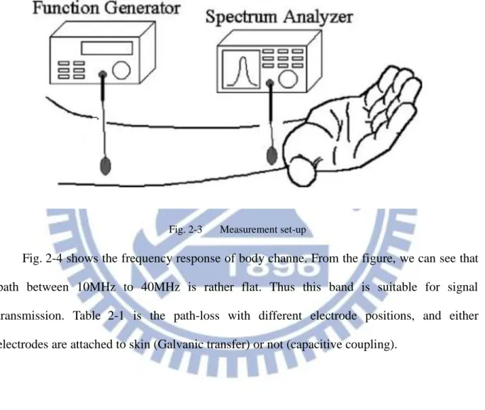
The path-loss of body channel changes with frequency and position of two electrodes. Fig. 2-3 shows the measurement set-up. Function generator transmits specific power with different frequencies, and we get received power from the spectrum analyzer. The difference between the power is the channel path-loss.
Fig. 2-3 Measurement set-up
Fig. 2-4 shows the frequency response of body channe. From the figure, we can see that path between 10MHz to 40MHz is rather flat. Thus this band is suitable for signal transmission. Table 2-1 is the path-loss with different electrode positions, and either electrodes are attached to skin (Galvanic transfer) or not (capacitive coupling).
9
Fig. 2-4 Frequency response
Table 2-1 Path-loss measurement Electrode Positions Path-loss (dB)
(Galvanic transfer / 1mm apart Capacitive coupling)
1 18.19 / 18.39 2 19.09 / 20.69 3 23.89 / 24.89 4 24.89 / 26.89 5 26.89 / 29.89 6 27.89 / 31.89
10 1 TX 2 3 4 5 6
2-1.4
Body Antenna Effect
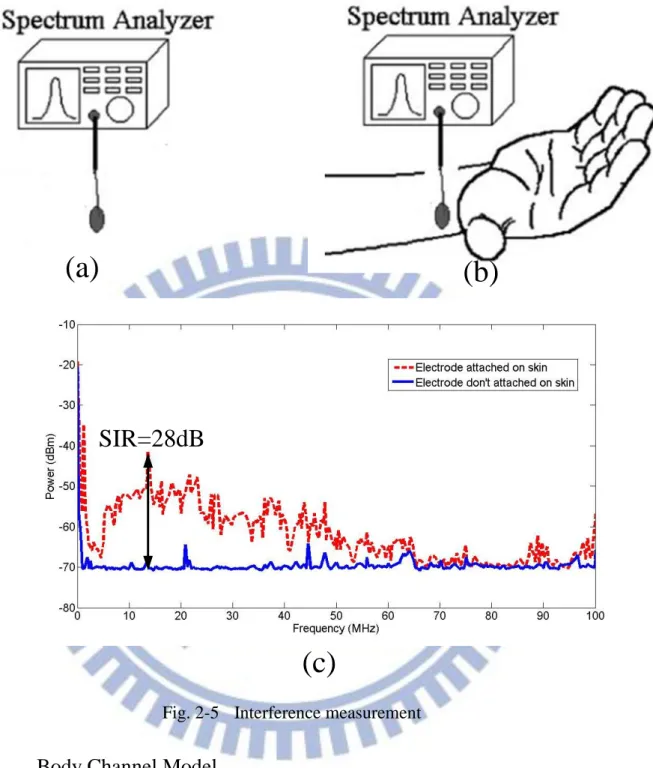
Human body is a lossy conductor with complex shape, thus it can be considered as wideband antenna [2], which is called body antenna effect. Since human body acts as a wideband antenna, it picks up surrounding radio signal, which degrades signal to interference ratio (SIR) in transmission. To measure the body antenna effect, the measurement set-up and result is shown in Fig. 2-5. Solid line is measure when electrode is not attached on human skin (a), dashed line is when electrode is attached on human skin (b). From the measurement, the maximum is about 28dB.
11
(a)
(b)
(c)
SIR=28dB
Fig. 2-5 Interference measurement
2-1.5
Body Channel Model
In document IEEE P802.15-08-0780-06-0006, it describes the scenarios for body area network, as shown in Fig. 2-6. Based on placement of communication nodes and transmission frequency, Table 2-2 lists all the scenario. From Fig. 2-6 and Table 2-2, we can find out that our proposed BCC falls into scenario S4 and S5, body surface to body surface, which belongs to channel model CM3.
12
Fig. 2-6 Body area network scenario Table 2-2 Body area network scenario
The channel model from IEEE P802.15-08-0577-01-0006 is composed of frequency response and noise characteristics, as shown in Fig. 2-7. The measurement result of frequency response is shown in Fig. 2-8, and noise characteristic is shown in Fig. 2-9. The mean is zero and variance is 2.55x10⁻⁵ and can be fitted into Gaussian distribution. The block diagram for channel model is shown in Fig. 2-10. Channel filter is the human body frequency response, which is valid between 0MHz to 50MHz, and the channel noise is the EM waves generated by electronic devices which couple into human body due to body antenna effect.
13
Fig. 2-7 Body channel model
14
Fig. 2-9 Noise characteristic Channel filter
Channel input
+
Channel noise
Channel output
Fig. 2-10 Channel model block diagram
The mathematical expression is shown in Equation
h
t
h
R
t
C
h( 2-1 ). where hR(t) is the channel impulse response and Ch is a coefficient related to sizes
of ground planes and distances between Tx and Rx.
t
h
R
t
C
h15
where
t
A
A
exp
t
t
/
t
sin
t
t
x
/
w
h
R
V
r 0
r
cAv represents the fluctuation of path-loss. It can be described by Gaussian distribution.
Av N(1, 0.16 2
)
The A, tr, t0, xc and w has constant values as follows:
2 5 / 49 . 120 782 . 0 0078 . 0 184 . 0 0422 . 0 body air body body R T h d d d d G G CGT and GR are the ground plane’s size(cm2) for TX and RX
dair and dbody are transmission distance through air and body.
The valid range are : 10cm2 GT, GR 270 cm 2
, 10 cm dair, dbody 200 cm
Following shows the matlab simulation with GT= GR =15 cm2 under different conditions.
Fig. 2-11 is when dair = dbody = 10cm, Fig. 2-12 is when dair = dbody = 30cm, and Fig. 2-13 is
when dair =100cm, dbody = 150cm.
Time range (s) A tr t0 xc w
0 t < 0.025 0.00032 0.00000 0.00621 -0.00097 0.00735 0.025 t < 0.058 0.00003 0.02500 0.01684 -0.01225 0.00944 0.058 t 0.00002 0.05800 0.05610 0.00100 0.01109
16
dair=10cm
dbody=10cm
Fig. 2-11 Channel with dair = dbody = 10cm
dair=30cm
dbody=30cm
17
dair=100cm
dbody=150cm
Fig. 2-13 Channel with dair =100cm, dbody = 150cm
2-2
Crystal-less Integration Issues
2-2.1
Crystal-less Integration Overview
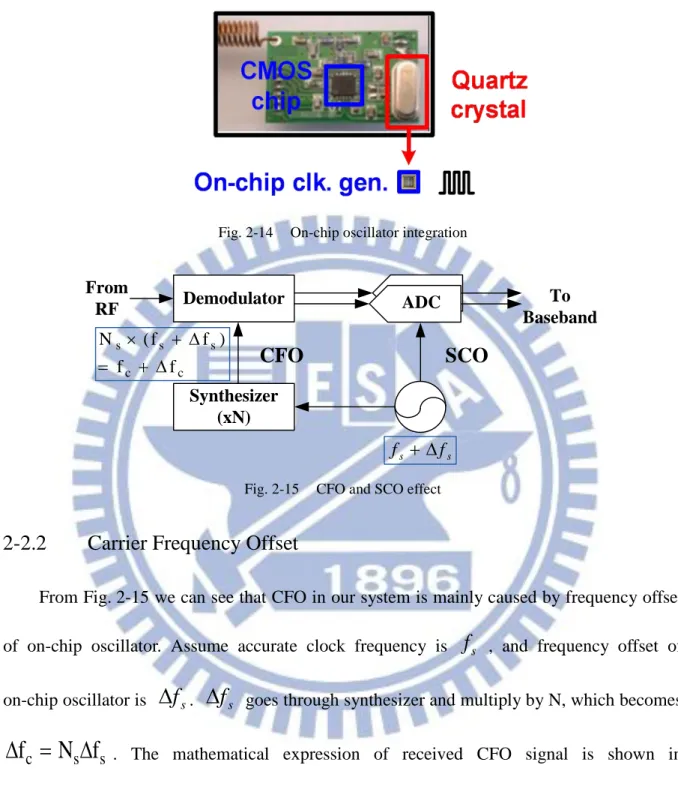
In Mobile Health-care application, for comfortable wearing of sensor nodes, we use on-chip oscillator integration (crystal-less) to replace large and bulky quartz crystal, as shown in Fig. 2-14. On-chip oscillator has supreme excess compared with quartz crystal oscillator in terms of area and process integration[6]. However, the frequency offset of the on-chip oscillator is larger than the tolerance of conventional packet-based OFDM system. This frequency offset of the on-chip oscillator causes carrier frequency offset (CFO) and sampling clock offset (SCO) in the system, as shown in Fig. 2-15.
18
Fig. 2-14 On-chip oscillator integration
ADC Demodulator Synthesizer (xN) s s f f c c s s s f f ) f f ( N
CFO
SCO
To Baseband From RFFig. 2-15 CFO and SCO effect
2-2.2
Carrier Frequency Offset
From Fig. 2-15 we can see that CFO in our system is mainly caused by frequency offset of on-chip oscillator. Assume accurate clock frequency is
f
s , and frequency offset ofon-chip oscillator is
f
s.
f
s goes through synthesizer and multiply by N, which becomess s
c
N
f
f
. The mathematical expression of received CFO signal is shown inequation( 2-2 ).
z
(t
)
is the received signal from RF, N is number of carrier, and Ng is number of cyclic prefix.
( 2-2 )
Frequency domain expression is equation( 2-3 )
S S g S g C nT T N T N N i t t f j n i
z
t
e
z
,
(
)
2|
( ) 19 k i k l N N j N N N N i j N k l l N l I f f l l l i N N j N N N N i j f f k k i k i V e e N k l N k l H X e e N N H X Z f I f I g g l f f I g g I Il , ) ( 1 ) ( ) ( 2 2 , 2 , 1 ) ( ) ( 2 , , ) ) ( sin( )) ( sin( ) sin( ) sin(
( 2-3 )We can express carrier frequency as
s f I c NT f (
) 1 , where
I is integer frequencyoffset, and
f is fractional frequency offset,0
.
5
f
0
.
5
k i k l N N j N N N N i j N k l l N l I f f l l l i N N j N N N N i j f f k k i k i V e e N k l N k l H X e e N N H X Z f I f I g g l f f I g g I Il , ) ( 1 ) ( ) ( 2 2 , 2 , 1 ) ( ) ( 2 , , ) ) ( sin( )) ( sin( ) sin( ) sin(
From equation(2.3) we can find out that I causes index shift as well as phase rotation.
fcauses magnitude attenuation, phase rotation, and ICI(second term in equation).
V
i,k is thechannel noise component.
2-2.3
Sampling Clock Offset
Sampling clock offset (SCO) happens when clock frequency of TX DAC and clock frequency of RX ADC are different. In our system, there is one accurate quartz crystal clock at CPN, and inaccurate on-chip oscillator at sensor nodes. Assume quartz crystal clock period equals to
T
s, and on-chip oscillator clock period equals to(
1
)
T
s, then we can express n-th received sample of i-th symbol as equation( 2-4 )20
( 2-4 )
The frequency domain expression is equation(2.5)
k , i 2 N k l , l 2 N l ] k l ) 1 [( N 1 N j l N N ) N N ( i 2 j l l , i k N 1 N j k N N ) N N ( i 2 j k k , i k , i V e e ) N ) k l ) 1 (( sin( N )) k l ) 1 (( sin( H X e e ) N k sin( N ) k sin( H X Z g g g g
( 2-5 )From the first term of equation
k , i 2 N k l , l 2 N l ] k l ) 1 [( N 1 N j l N N ) N N ( i 2 j l l , i k N 1 N j k N N ) N N ( i 2 j k k , i k , i V e e ) N ) k l ) 1 (( sin( N )) k l ) 1 (( sin( H X e e ) N k sin( N ) k sin( H X Z g g g g
( 2-5 ), we can see clock offset
causes magnitude attenuation and phase rotation. Phase rotation is proportional to k and index i, which means phase rotation becomes larger at later symbol. Second term is inter-carrier interference.V
i,k is the channel noise component.S S g S g T N T n T N N i t n i
z
t
z
,
(
)
|
( )(1) (1) (1)21
Chapter 3:
Design of Crystal-less OFDM-based
Transceiver Baseband
3-1
OFDM Transmission Strategy
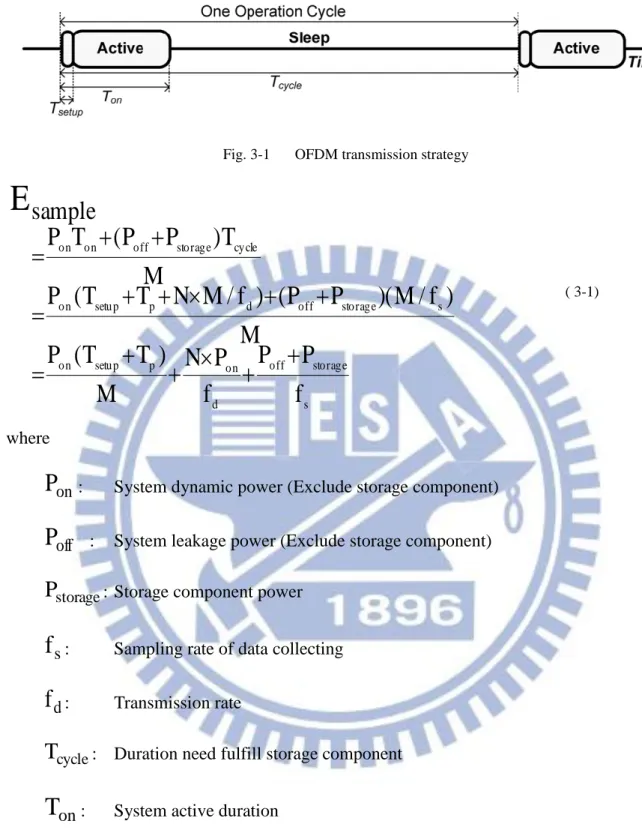
OFDM has been a very popular modulation for high data-rate transmission. Moreover, we further take the high data-rate advantage of OFDM to reduce the overall transmission energy. From Fig. 3-1, we can explore the low energy strategy behind packet-based OFDM. When in sleep mode, only the storage component of the system operates, and other blocks are turned into sleep mode (power gated). While the data is collected to certain amount, system turns into active mode, and transmit the data in one shot. Therefore it uses high data-rate transmission ability of OFDM to reduce the operation time of transmission blocks, thus reducing the overall operation energy. Mathematical analysis is shown in Equation
s storage off d on p setup on s storage off d p setup on cycle storage off on on
f
P
P
f
P
N
M
)
T
T
(
P
M
)
f
/
M
)(
P
P
(
)
f
/
M
N
T
T
(
P
M
T
)
P
P
(
T
P
sample
E
( 3-1)22
Fig. 3-1 OFDM transmission strategy
s storage off d on p setup on s storage off d p setup on cycle storage off on on
f
P
P
f
P
N
M
)
T
T
(
P
M
)
f
/
M
)(
P
P
(
)
f
/
M
N
T
T
(
P
M
T
)
P
P
(
T
P
sample
E
( 3-1) where onP
: System dynamic power (Exclude storage component)off
P
: System leakage power (Exclude storage component)storage
P
: Storage component powers
f
: Sampling rate of data collectingd
f
: Transmission ratecycle
T
: Duration need fulfill storage componenton
T
: System active durationsetup
T
: Setup time from sleep to activep
23
3-2
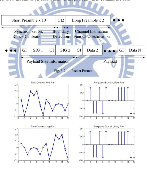
OFDM Packet Format
Fig. 3-2 is packet format of our system. It is combination of 10 identical short preambles (Fig. 3-3), which is used for synchronization and clock calibration. GI2 is the last 32 points of long preamble, we uses GI2 for boundary detection. Following is 2 identical long preambles(Fig. 3-4) which are used for channel estimation and fine-CFO estimation. Two SIG packets show the size of payload. Finally is the payload which contains the data.
Short Preamble x 10 GI2 Long Preamble x 2
SIG 1
GI GI SIG 2 GI Data 2 GI Data N
Synchronization, Clock Calibration Boundary Detection Channel Estimation Fine-CFO Estimation
Payload Size Information Payload Fig. 3-2 Packet Format
24
Fig. 3-4 Long Preamble
3-3
Proposed Crystal-less OFDM-based Transceiver Baseband
3-3.1
Baseband Overview
Fig. 3-5 shows the proposed BCC transceiver baseband. At TX baseband, mapper maps bitstream into QPSK symbol. Then IFFT transfer symbol from frequency domain to time domain. In time domain, CP is added in front of each symbol. Finally the preamble and SIG are added at beginning of the packet.
At RX baseband, after packet is detected, AGC calculates the power and sends the codeword to DVGA to tune the gain of it, and CLK drift estimator estimates the clock offset and sends the corresponding codeword to on-chip oscillator to tune the frequency. After the clock is calibrated, packet goes through boundary detection, which uses dual-correlation algorithm.
25
After boundary is detected, the following payload transform to frequency domain. In frequency domain, it further does post-FFT compensation before de-mapping QPSK into bit-stream.
Packet Detection & AGC CLK Drift Estimator Boundary Detection FFO Etimator FFO De-Rotator FFT Channel Equalization Post FFT Comp. Demapper Bitstream Mapper IFFT Add CP Add Preamble and SIG M U X Bitstream
To DVGA To On-Chip Osc.
TX Baseband RX Baseband TX Front-end RX Front-end Electrode
Fig. 3-5 Transceiver Baseband Block Diagram
3-3.2
Synchronization and Clock Calibration
Detection
Equation ( 3-2 ) shows the algorithm for packet detection. The basic idea behind algorithm is auto-correlation. In our design, we aim to detect the coming of two repetitive short preambles, so R = 16, L = 16. The short preamble is designed to be pseudo-noise, so the peak shows up when two symbols are the same. Fig. 3-6, shows the waveform when short preamble shows up. In our packet format, there are 10 repetitive short preambles, so the waveform looks like plateau when short preamble comes in. The packet is detected when auto-correlation is larger than pre-defined threshold, as shown in Fig. 3-6. ( 3-2 )
|
|
)
(
1 0 *
R r m r m r Lz
z
m
26
Threshold
Packet Detected
Short Preamble x 10
Fig. 3-6 Auto-correlation Waveform
Auto Gain Control
As described in chapter 2-1.3, path-loss of body channel changes as transmission types (Galvanic transfer or capacitive coupling), different position of electrodes, and transmission frequency. Thus Auto Gain Control (AGC) is needed in order to remain swing of input signal, which will influence BER performance of system. Equation( 3-3 ) shows the equation for AGC. When packet is detected, AGC compare the input signal power with ideal signal power, thus calculating the needed gain. Then AGC converts the gain into corresponding codeword to tune digital variable gain amplifier (DVGA). Fig. 3-7 is the flow chart of AGC.
( 3-3 )
|
|
|
|
1 0 * 1 0 * ) (
R r m r m r L R r m r m r L Threshold mx
x
z
z
Gain
27
Packet Detection
Auto Gain Control
Detected?
Tune DVGA
YES NO
New Packet Coming
Fig. 3-7 AGC Flow Chart
Clock Drift Estimator
When there is frequency offset in the oscillator, it will cause sampling clock offset (SCO), and then go through synthesizer, and become carrier frequency offset (CFO). Thus we can extract oscillator frequency offset from CFO, and then send corresponding codeword to tune the oscillator. Fig. 3-8 is the block diagram for clock drift estimator. After packet detection and AGC, estimator I uses the short preambles to calculate the fractional frequency offset. Then de-rotator rotates the short preambles phase due to value from estimator I. After de-rotation, short preamble comes into estimator Ⅱ. Total frequency offset equals to combination of value calculated by estimator I and estimator Ⅱ . Then DDFS tuning codeword mapping maps the calculated frequency offset to corresponding DDFS codeword.
28
Estimator I De-Rotator Estimator Ⅱ
DDFS Tuning Codeword Mapping Clock Drift Estimator DDFS Tuning Codeword Packet Detection & AGC Boundary Detection
Fig. 3-8 Clock Drift Estimator Estimator I
Here we use maximum likelihood estimation to calculate CFO, as shown in Equation(3.5). Zm in the equation is the short preamble.
Fig. 3-9 is the estimation offset when clock offset equals 4000ppm. It shows that estimation value oscillates around real offset value, thus we take the mean of estimation value over a sequence. The overall clock offset is shown in Equation( 3-4 ).
Phase can only resolve in range of
, which corresponds to ideal estimation range equals tos
LT
2 1
. Since the baseband data also suffer from SCO, the actual estimation range will smaller than
s
LT
2 1
. From Matlab simulation (Fig. 3-9), when TS is 5MHz, the toleration
of algorithm is 4000ppm. ( 3-4 ) ( 3.5 ) S S g S g C nT T N T N N i t t f j e t z n i z, ( ) 2
| ( ) )}
z
z
(
LT
2
1
{
avg
N
1
c
f
*m r L 1 R 0 r r m s
29 (a)
ppm
4000
(b)Fig. 3-9 Matlab simulation of clock drift estimation
Estimator Ⅱ
We use Estimator Ⅱto estimator larger frequency offset. Estimator Ⅱuses match filter approach to detect the specific frequency offset. As shown in Fig. 3-10 and Equation( 3-5 )
H0: x[n] = s0[n] + w[n]
Hi : x[n] = si [n] + w[n]
Hk: x[n] = sk[n] + w[n] ( 3-6 )
where
si[n]:Detector with different IFO, n= 0~N-1
w[n]:White Gaussian noise, n = 0~N-1 The probability under white Gaussian noise is
30
The optimal Hi is chosen when
Thus the optimal decision is
1 0 N n S0[n] 1 0 N n Si[n] 1 0 N n Sk[n]
…
…
Selection
of
Maximum
X[n]Fig. 3-10 Phase Ⅱ Estimator
Short preamble is the prior knowledge to the RX. To get si[n] detector, we pre-distort the
short preamble with specific frequency offset, as shown in Fig. 3-11. For example, to get 8000ppm detector, we pre-distort short preamble with 8000pppm frequency offset.
2 1 N 0 n i 2 2 N 2 i
x
[
n
]
s
[
n
]
)
2
1
exp(
)
2
(
1
)
H
|
x
(
p
N 1 0 n 2 i 2 i(
x
[
n
]
s
[
n
])
D
))
]
n
[
s
]
n
[
x
(max(
arg
H
ˆ
1 N 0 n i i i
31 f fs
Short Preamble
s
i[n]
Fig. 3-11 Generation of detector coefficient
De-Rotator
Estimator Ⅱ decides the frequency offset according to smallest distance between incoming distorted short preamble and specific detector si[n]. To make incoming short
preamble closer to the si[n], de-rotator compensates the short preamble due to the value from
estimator I. The overall procedure is shown in Fig. 3-12. Assume original short preamble has -9000ppm frequency offset. Ideally, estimator I gets value -1187.5ppm, and de-rotator compensate this frequency offset, making the remaining frequency offset locate on -8000ppm detector. Finally the total frequency offset is combination of estimated value from estimator I and estimator Ⅱ, which is -1187.5ppm + -8000ppm equals -9000ppm.
S
0S
1S
2S
-1S
-2-9000ppm
-1187.5ppm -15625ppm Detector -7812.5ppm Detector 0ppm Detector 7812.5ppm Detector 15625ppm Detector Fig. 3-12 Clock calibration example32
Boundary Detection
After the packet detection, we get the rough timing information of coming packet. However, we still need further timing information in order to derive ISI-free DFT-window for later channel estimation, SIG decoding, and data demapping.
Conventional boundary detection uses cross-correlation algorithm Equation( 3-7). The receiver correlates the received signal with ideal pre-known waveform (such as GI2 in preamble). The boundary is found when cross-correlation value is larger than threshold, as shown in Fig. 3-13
( 3-7 )
Threshold
Boundary
Fig. 3-13 Conventional cross-correlation
However, frequency offset of on-chip oscillator deteriorates the received signal, which decreases the correlation value significantly. Moreover, the multipath effect causes the uncertainty of the peak of correlation value as shown in Fig. 3-14.
|
|
)
(
1 0 *
R r L r m r mx
z
m
33 First arrive path Last arrive path
Fig. 3-14 Multipath effect
Due to the above problems, we use dual-correlation algorithm to do the boundary detection. It combines both auto-correlation and cross-correlation algorithm, and in auto-correlation part, it averages over some short preamble symbols to combat the magnitude attenuation due to clock frequency offset. The boundary detection algorithm is shown in Equation( 3-8 ). z is the received signal. x is the ideal short preamble. N is short preamble size 16. R is the auto-correlation window which equals to 16.
( 3-8 )
Boundary is detected when
The waveform is shown in Fig. 3-15
1 0 1 0 *|
|
)
(
L l R r L r m N l r m N lz
z
m
|
|
)
(
1
0
*
R
r
L
r
m
r
m
x
z
m
2
_
)
(
1
_
)
(
Threshold
L
m
Threshold
m
34
Boundary Detected
Threshold_1 Threshold_2
Fig. 3-15 Dual correlation waveform
3-3.3
Channel Equalization
The measurement result in Fig. 3-16 shows that body channel is selective, thus we need channel equalizer to make it flat. The algorithm we choose is zero forcing, as shown in equation( 3-9 ). We use received long preamble, compared it with ideal long preamble. The comparison result is estimated channel. Then the incoming signal divided by estimated to make it response flat.
35
Fig. 3-16 Frequency response
( 3-9 )
Ck = channel frequency response
LPk = ideal long preamble
LP’k = received long preamble
Zk = incoming signal
Z’k = signal after equalization
3-3.4
Post-FFT Compensation
In the time domain, we have done the clock calibration and fine carrier frequency offset calibration. However, due to noise, clock jitter, and some other defects, there still exists some residual offset in the system. Thus post-FFT compensation is needed. Equation( 3-10 ) shows the frequency domain expression when there is residual offset exists.
ε
F is carrier frequency offset (CFO), andδ
S is sampling clock offset(SCO). From equation( 3-10 ) we can see thatCFO and SCO causes phase shift for received signal, thus the distortion in phase is in equation ( 3-11), k is the sub-carrier index.
( 3-10 )
( 3-11 )
Fig. 3-17 shows the frequency domain plot of phase. From the figure, we can see that CFO causes offset in phase and SCO results into slope in phase.
k
C
k
Z
k
Z
k
LP
k
LP
k
C
/
'
/
'
] ) kδ (ε ) ( [ 2 2 , , S F]
)
sin(
)
sin(
)
sin(
)
sin(
[
N N N N i j S F S F k k i k i g ge
N
k
N
N
k
H
X
Z
)
kδ
(ε
F
S
k
36
F
S
Fig. 3-17 Phase distortion in frequency domain
Here we use linear least square estimation to calculate the residual CFO and SCO. We can model distorted phase as equation ( 3-12 ). The linear least square estimation solution is shown in equation( 3-13 )
( 3-12 )
( 3-13 )
Because phase can only resolve into
,
s gLN
sN
g k
N
k
T
N
LN
f
2
(
)(
1
)
2
(
)
k T T S F S F kH
H
H
H
1 ' ')
(
,
)
1
...(
...
0
1
...
1
...
1
N
k
H
37
where
f
f
c
f
c' , in our systemT
S = 5MHz andf
c = 20MHz Thus
f
4
(
f
s
f
s')
' ' ' ' '1
1
1
1
1
1
s s s s s s sf
f
f
f
f
f
f
T
T
T
s s g sLN
sN
g k
N
k
f
N
LN
f
2
(
4
')(
)(
1
)
/
2
(
)
Since we compensate symbol by symbol, thus L = 1
In our system, sub-carrier size N = 64, cyclic prefix Ng = 4, k = 31,
k
0
Assumef
s
f
s' Thus
s g sLN
sN
g k
N
k
N
LN
2
(
4
)(
)(
1
)
2
(
)
Take all the numbers in
38
3-4
Simulation Result
Fig. 3-18 is the matlab simulation model. Here we use the body channel model from IEEE P802.15-08-0577-01-0006. Then AWGN is added to the signal and multiply CFO rotation. Finally using Resample to simulate SCO effect.
TX Baseband Body Channel Model AWGN ej2ft CFO Resample SCO RX Baseband
Fig. 3-18 Matlab simulation model
Fig. 3-19 shows the matlab simulation result with different initial clock offsets. Line with round marker corresponds to 0ppm clock offset, line with triangle marker corresponds to 10000ppm clock offset, and line with square marker corresponds to 20000ppm clock offset. Simulation result shows that there are a little BER degrade when clock offset gets larger and larger.
39
Chapter 4:
Implementation of Transceiver
Fig. 4-1 is the overall architecture for OFDM-based BCC transceiver, and Fig. 4-2 is the corresponding picture. It contains TX front-end, RX-front-end, and TRX baseband. TX baseband pattern feeds into DACs. DACs converts digital pattern to analog signal. According to human body frequency response, around 20MHz, channel response is flat and path-loss is small, which is suitable band for transmission. Thus modulator up-converts baseband signal to 20MHz. Then the driver matches the impedance of system to impedance of electrode. The TX signal is connected to body through electrode attached on skin. RX also uses electrode to collect transmitted signal from body. The DVGA tunes the input signal to certain voltage level, which is suitable for demodulation and later DSP processing. The collected signal is down-converted by demodulator to baseband. The baseband signal then goes through ADCs and is converted to digital signal and feed to RX baseband.
ADC DAC Modulator Demodulator Driver DVGA Synthesizer DDFS E-Crystal Chip TX BB RX BB TX Front-end RX Front-end TRX Baseband
40
TX Front-end
RX Front-end
TRX
Baseband
41
4-1
Transmitter Front-end
3
2
1
4
5
5
Fig. 4-3 Transmitter front-end picture, number 1 is DAC, number 2 is Mod, number 3 is Driver, number 4 is Power IC.
Table 4-1 Transmitter front-end components
Block Number Function Component Specifications
1 DAC AD9765 12bits / 5MHz
2 Modulator LTC5598 RF 20MHz
3 Driver LMH6515 200 Ohm
4 Power IC RT9047 3.3V
42
Fig. 4-3 is the picture of transmitter front-end, and Table 4-1 is the corresponding components table. Here we choose dual channel DAC. Its inputs are I and Q digital codeword, and outputs are I and Q differential analog waveform. Because the modulator baseband inputs are PNP BJTs with 0.5V DC bias, we add an offset in digital codeword to make DAC outputs have 0.5V DC bias. The modulator up-converts baseband signal to 20MHz RF signal and then feed RF signal to driver. From [7](Fig. 4-4), we can see that contact impedance of human body with different metal electrodes. at 20MHz, is around 200 Ohm, thus the drive with 200 Ohm output impedance is chosen to match the contact impedance.
Fig. 4-4 Impedance frequency response
Since the device is designed to be portable, thus in power planning, besides from normal DC plug input, it can also uses battery as power input. The schematic of power planning is shown in Fig. 4-5
43
Power supply from battery
Power supply DC plug input
DC to power IC
44
4-2
Receiver Front-end
1
2
3
4
5
6
7
Fig. 4-6 Receiver front-end picture, number 1 is DVGA, number 2 is Demod, number 3 is ADC, number 4 is Power IC, number 5 is Synthesizer, number 6 is DDFS, number 7 is e-Crystal socket
Table 4-2 Receiver front-end components
Block Number Function Component Specifications
1 DVGA AD9765 200 Ohm
2 Demodulator AD8333 RF 20MHz
3 ADC AD9235 12bits / 5MHz
4 Power IC RT9047 RT9183 LT3032 3.3V / 5V / 1V 5 Synthesizer AD9913 80MHz
6 DDFS AD9913 Tuneable frequency
7
e-Crystal socket
45
Fig. 4-6 is the picture of transmitter front-end, and Table 4-2 is the corresponding components table. From chapter 2.1-3, we know that path-loss varies with transmission scheme and transmission distance. Thus a DVGA is included in the system. The gain of DVGA is controlled by baseband digital codeword, which is calculated by VGA block. Also, the input impedance of DVGA is 200 Ohm to match the contact impedance of human body with electrode. The demodulator down-converts the 20MHz RF signal to baseband signal. Specially note that local oscillator (LO) of demodulator should be 4 times the RF frequency. For example, 20MHz RF signal should have LO frequency equals to 80MHz. Following is ADC to transfer analog waveform into digital codeword for baseband processing. To emulate with e-Crystal chip, 32-DIP socket is included. The e-Crystal clock feeds to DDFS, which is frequency tunable with digital codeword from baseband clock calibration block.
There are two important issues in layout of PCB, symmetry and shielding. OFDM system has I and Q channel, symmetric layout for those two channels is very important. IQ imbalance
Following is the analysis of IQ imbalance in OFDM system. Fig. 4-7 is the basic block diagram for direct-conversion receiver.
LPF
LPF
)
t
f
2
cos(
c)
t
f
2
sin(
c
)
t
(
y
~
)
t
(
x
~
I)
t
(
x
~
Q Fig. 4-7 Direct conversion receiver46
Ideally the passband signal can be expressed as Equation (4-1)
)
t
f
2
sin(
)
t
(
x
)
t
f
2
cos(
)
t
(
x
}
e
)
t
(
x
Re{
)
t
(
y
j2fct
I
c
Q
c
( 4-1 )Assume system exists gain error
1
1 and phase error , we model those imbalance into
LO, and the express the LO output as equation(4-2)
) 2 t f 2 sin( ) 1 ( 2 ) 2 t f 2 cos( ) 1 ( 2 c c ( 4-2 )
Thus the baseband signal due to imbalance is
) t ( Bx ) t ( Ax ) t ( x )] 2 sin( j ) 2 cos( [ ) t ( x )] 2 sin( j ) 2 [cos( ) t ( x ~ j ) t ( x ~ ) t ( x ~ )] 2 sin( x ) 2 cos( ) t ( x )[ 1 ( ) t ( x ~ )] 2 sin( x ) 2 cos( ) t ( x )[ 1 ( ) t ( x ~ * * Q I I Q Q Q I I ( 4-3 )
To analyze the effect in frequency domain, we know that
(
X
k)
*
X
*k Thus * k k kAX
BX
X
~
( 4-4 )From Equation(4-4), we can see that IQ balance in frequency domain not only has complex gain on the carrier, but also introduces ICI to the carrier.
Fig. 4-8 shows a time domain short preamble waveform, blue waveform is from I channel and green waveform is from Q channel, which has IQ gain mismatch around 1dB.
47
Fig. 4-8 IQ gain mismatch
To combat this problem, we reserve path for attenuator on I and Q, and manually tune the gain by inserting attenuator in I and Q path, as shown in Fig. 4-9. For example, if measurement result shows that I channel is 1dB larger than Q channel, then we insert 1dB attenuator in I channel and 0dB attenuator in Q channel to make two path balance.
I channel attenuator
Q channel attenuator
48
RF shielding
In our system, there are many components with different operation frequency. To avoid interference from each other, carefully RF shielding is needed. Fig. 4-10 shows demodulator output short preamble waveform with RF coupling interference from LO.
600mVpp
137mVpp
Fig. 4-10 Coupling interference
To combat this problem, we add many via along the RF path and PCB board to avoid the coupling interference, as shown in Fig. 4-11.
Via shielding
49
4-3
Emulation of Clock Drift Calibration
The emulation flow of clock drift calibration is shown in Fig. 4-12. Assume originally there is clock drift in e-Crystal chip, which is 0.020MHz drift from ideal 5MHz clock frequency. This drifted clock feed into DDFS. The output of DDFS servers as ADC reference input and synthesizer input. The synthesizer multiplies input frequency by 5 times, which makes LO frequency of Demodulator equals 80.32MHz. When preamble comes into system, clock calibration block in RX BB calculates the frequency offset, and then sends corresponding DDFS tuning codeword to tune the DDFS. After DDFS receive digital tuning codeword, its frequency is tuned to be 5MHz, thus compensates the clock drift from e-Crystal chip.
ADC
Demodulator
DVGA
Synthesizer
DDFS
RX BB
e-Crystal
Chip
DDFS Tuning Codeword 5.020MHz 5.020MHz => 5MHz 80.32MHz => 80MHzFig. 4-12 Clock calibration emulation flow
The emulation result is shown in Fig. 4-13. Fig. 4-13 (a) is the initial DDFS output before calibration, Fig. 4-13 (b) is the initial DDFS output after calibration. Fig. 4-14 (a) is the short preamble output before calibration, Fig. 4-14(b) is the short preamble output after calibration.
50
We can see form those figures that before calibration, there is clock frequency offset and the short preamble pattern is distorted. After calibration, the clock frequency is corrected and the short preamble is restored.
5MHz
5.020MHz
(a)
(b)
51
(a)
(b)
52
4-4
Emulation of AGC
Fig. 4-15 is the emulation flow of AGC. Assume initially the input voltage swing is smaller than expected. The VGA block in RX BB calculates the gain using the input preamble, and according to the gain, sends the corresponding DVGA tuning codeword to tune the gain of DVGA. ADC Demodulator DVGA Synthesizer DDFS RX BB e-Crystal Chip
DVGA Tuning Codeword
Fig. 4-15 AGC emulation flow
Fig. 4-16 shows the emulation result. Originally, input short preamble voltage swing is smaller than expected. After tuning DVGA, the swing goes to expected value.
Tuning DVGA
53
Chapter 5:
Experiment Result
5-1
Measurement Result
This chapter shows the experiment result. Fig. 5-1 is the TX DAC output. The format of the waveform is also shown below. Then Fig. 5-2 is the TX MOD output. We can clearly see that the waveform contains high frequency part, which is waveform in Fig. 5-1 modulating with 20MHz sin wave. Fig. 5-3 is the RX ADC output. It has a little distortion, which comes from noise and interference. Fig. 5-4 is the received baseband signal. The baseband word length is 8 bits and word depth is 9 bits. The detection of arriving of the packet is done when receiver baseband receives 10 repetitive short preambles. Then the AGC, and clock calibration process after packet detection. GI2 is used for boundary detection. Following is 2 identical long preambles which are used for channel estimation and fine-CFO estimation. Two SIG packets show the size of payload. Finally is the payload which contains the data.
Short Preamble x 10 Long Preamble x 2 G I 2 SIG 1 G I SIG 2 G I DATA G I
54
Fig. 5-1 DAC output
Short Preamble x 10 Long Preamble x 2 G I 2 SIG 1 G I SIG 2 G I DATA G I
55 Short Preamble x 10 Long Preamble x 2 G I 2 SIG 1 G I SIG 2 G I DATA G I
Fig. 5-3 ADC output
Short Preamble x 10 Long Preamble x 2 G I 2 SIG 1 G I SIG 2 G I DATA G I
56
Fig. 5-5 is the experiment result under different conditions. In condition 1 and condition 2, two sensors are attached on one arm with distance 10cm and 30cm, and the BER
performance of these two conditions is close to each other. However, when two sensors are across arm, as shown in condition 3, the BER degrades a lot. This is probably due to when two sensors are far from each other, the interference comes from body antenna effect is more severe.
57 10cm 30cm
Condition 1
Condition 2
Condition 3
150cmBER=7x10
-3BER=8x10
-3BER=3x10
-258
5-2
Comparison Result
Table 5-1 is the comparison of BCC systems. It compares modulation scheme, frequency band, data rate, and oscillator type. From the comparison, we can see this work achieve high data rate with better spectral efficiency, and on chip oscillator integration to provide smaller area and more comfortable wearing. The all digital e-Crystal on-chip oscillator is portable with process migration.
Table 5-1 Compared with other BCC systems
Publication This work ISSCC’07[1] JSSC’09[3] ASSCC’10[13]
Modulation OFDM PAM FSK FSK
Freq. Band (MHz) 17.5 ~ 22.5 1 ~ 200 30 ~ 70 20 ~ 40 Data Rate (Mbps) 6.7 2 5 1 Spectral Efficiency
(bps/Hz) 1.34 0.01 0.125 0.05
Oscillator e-Crystal
(All digital) All digital LC DCO LC DCO Process Migration Portable Portable Non-Portable Non-Portable