國
國
國
國
立
立
立
立
交
交
交
交
通
通
通
通
大
大
大
大
學
學
學
學
光電工程研究所
光電工程研究所
光電工程研究所
光電工程研究所
碩
碩
碩
碩
士
士
士
士
論
論
論
論
文
文
文
文
不同電極對下電極結構之非晶系銦鎵鋅氧
薄膜電晶體之影響
Effects of Source and Drain Electrode Types on
Bottom Contact Amorphous-Indium-Gallium-Zinc-Oxide
Thin-Film Transistors
研
研
研
研
究
究
究
究
生
生
生
生:
:
:
:吳高銘
吳高銘
吳高銘
吳高銘
指導教授
指導教授
指導教授
指導教授:
:
:
:謝漢萍
謝漢萍
謝漢萍
謝漢萍
教授
教授
教授
教授
中
中
中
中
華
華
華
華
民
民
民
民
國
國
國
國
九
九
九
九
十
十
十
十
八
八
八
八
年
年
年
年
六
六
六
六
月
月
月
月
不同電極對下電極結構之非晶系銦鎵鋅氧
薄膜電晶體之影響
Effects of Source and Drain Electrode Types on
Bottom Contact Amorphous Indium-Gallium-Zinc-Oxide
Thin-Film Transistors
研 究 生:吳高銘 Student:Gao-Ming Wu
指導教授:謝漢萍 Advisor:Han-Ping D. Shieh
國立交通大學 電機學院
光電工程研究所
碩 士 論 文
A ThesisSubmitted to the Institute of Electro-Optical Engineering College of Electrical and Computer Engineering
National Chiao Tung University in partial Fulfillment of the Requirements
for the Degree of Master in
Electrical-Optical Engineering June 2009
Hsinchu, Taiwan, Republic of China
不同電極對非晶系銦鎵鋅氧薄膜電晶體之影響
學生:吳高銘
指導教授:謝漢萍
國立交通大學光電工程研究所
摘
要
摘
摘
要
要
摘
要
藉由探討氧通量,退火,半導體與介電層介面性質,與不同電極材料的 變化,研究了不同製程因素對於銦鎵鋅氧薄膜的特性影響,以提升非晶系 銦鎵鋅氧薄膜電晶體的效能。一開始,先藉由氧通量的變化,來探討氧通 量對薄膜特性的影響,而優化薄膜的半導體特性。另一方面,藉由退火改 善了半導體與介電層的介面特性,結果隨著退火時間增長,臨界電壓會減 小。進一步的,藉由引入介面修飾層,來探討半導體與介電層介面特性, 找出適合銦鎵鋅氧的接觸面性質,而發現疏水性的 HMDS 改善了載子遷移 率。接下來,藉由探討不同電極材料之功函數與接觸阻抗的關係,對下電 極結構之非晶系銦鎵鋅氧薄膜電晶體效能的影響,進而找出適合匹配銦鎵 鋅氧的電極材料,用來改善非晶系銦鎵鋅氧薄膜電晶體的效能,結果鈦電 極展現了最佳的特性。最後,因為不具通道保護層的裝置會與環境中的水氧 反應,而進一步討論了臨界電壓隨時間減小的不穩定性。
Effects of Source and Drain Electrodes on
Amorphous Indium-Gallium-Zinc-Oxide
Thin-Film Transistors
Student::::Gao-Ming Wu
Advisor::::Dr. Han-Ping D. Shieh
Institute of Electro-Optical Engineering National Chiao Tung University
ABSTRACT
Via investigating the oxygen and annealing effects, interface property, and source/drain materials, high performance a-IGZO TFT was fabricated. First, the oxygen flow rate was varied to examine oxygen absorption effect. Post-annealing improves the bonding in a-IGZO because of the semiconductor/insulator interface modification. The device mobility can be up to 11.42 cm2(Vs)-1. Second, the dual stack a-IGZO TFT structure is introduced to examine the properties of the a-IGZO/gate insulator interface. HMDS-buffered a-IGZO TFT has larger mobility, implying improved channel/dielectric interfacial condition when it is stacked with the hydrophobic material HMDS. Following, the effects of source/drain electrode types on a-IGZO TFT were investigated. The performance of the a-IGZO TFT with Ti source/drain electrodes is appropriate for the display applications. Finally, the ambient effect was discussed. The water molecule absorption dominates the a-IGZO ambient interaction in ambience and the threshold voltage shifts negatively.
誌
謝
誌
謝
誌
謝
誌
謝
首先要感謝指導教授謝漢萍院長為我們建立了一個資源豐富的研究環 境,兩年的碩班生涯著實令我受益良多。除了設備完善讓我們可以有世界 級的研究成果,高水準的的師資與研究團隊可以隨時與世界頂尖研究成果 爭雄,實驗室注重英文能力等精神也讓我們不忘踏出關門研究的階段,培 養國際化的視野,成為更全方位的人才,可以在未來為校爭光,回饋培育 我們的社會。另一方面也感謝黃乙白教授與鄭惟中教授的照顧,與華映及 交映樓學長同學們的幫忙。 在實驗的過程中我最感謝我的好夥伴朱益興。他與我在無塵室內,量測 機台邊共度無數時光。有漫漫長夜,有破曉時分,擁有得來不易的令人欣 慰的成果時,喜悅可以共享。也感謝學長莊喬舜也不時給關心我們並給予 指點並有情有義的帶著我們畢業。 最後最重要的,我要感謝的父母家人,他們的養育之恩, 栽培之情,與 不離不棄的陪伴, 比任何言語都要深刻而有力的支持著我, 我會用一切 的努力來報答。
Table of Contents
Abstract (Chinese)………i
Abstract (English)………...….ii
Acknowledgements……….…iii
Table of Content………..iv
Figure Caption………..……....v
List of Tables……….……..vi
Chapter 1 Introduction………..13
1.1. Amorphous Semiconductors………131.2. Amorphous Oxide Semiconductors……….15
1.2.1. The Introduction to Amorphous Oxide Semiconductors………..…15
1.2.2. The Carrier Transport Mechanism of AOSs………..16
1.3. Amorphous In-Ga-Zn-O Thin Film Transistors………17
1.3.1. Introduction...17
1.3.2. The In2O3-Ga2O3-ZnO Ternary System………...18
1.3.3. The a-IGZO TFT State of the Art………...22
1.4. Motivation ………...25
1.5. Thesis Organization ………...26
Chapter 2 Principles and Characterization………...27
2.1. Thin Film Transistor and Operation………...27
2.2. Electrical Measurement………..30
2.3.1. Determination of the Threshold Voltage………...30
2.3.2. Determination of the Subthreshold Swing………...31
2.3.3. Determination of the Field-Effect Mobility………32
2.3.4. Determination of the On/Off Current Ratio………...33
2.4. Surface Morphology Measurement………...33
2.5. Contact Angle Measurement………..35
Chapter 3 Experimental Methods………..37
3-1. a-IGZO TFT Device Fabrication………...37
3-2. Sputtering………...30
3.2.1. RF sputtering………...41
3.2.2. DC sputtering………...42
Chapter 4 Experimental Results and Discussion………..44
4-1. The Effects of Oxygen Flow Rate and Post-Annealing on a-IGZO TFTs……...44
4.1.1. Introduction………...44
4.1.2. Results and Discussion………...47
4.1.2.1. Determination of the Deposition Rate………...47
4.1.2.2. The Effects of Oxygen Flow Rate on a-IGZO TFTs………...48
4.1.2.3. The Effects of Post-Annealing on a-IGZO TFTs ………...51
4.1.3. Conclusion………...52
4-2. The Interface Modification for a-IGZO TFTs………....53
4.2.1. Introduction………...53
4.2.2. Result and Discussion ………...54
4.2.3. Conclusion ………...57
4-3. The Effects of Source and Drain Electrodes on a-IGZO TFTs………...58
4.3.1. Introduction ………...58
4.3.2.1. The Effects of Source/Drain electrodes on a-IGZO TFTs ………...60
4.3.2.2. The Ambience Effect on a-IGZO TFTs………...64
4.3.3. Conclusion ………...68
Chapter 5 Conclusion………...70
5-1. Conclusion………...70
5-2. Future Work………...72
Figure Caption
Fig. 1-1 History of amorphous semiconductors on new fields………..2
Fig. 1-2 Flexible transparent TFTs (TIFTs) (a) A photograph of the flexible TIFT sheet bent at R = 30 mm. The TIFT sheet is fully transparent in the visible light range (b) A photograph of the flexible TIFT sheet. The transparent TFT devices are made visible by adjusting the angle of the illumination2...3
Fig. 1-3 Schematic orbital drawing of electron pathway (conduction band bottom) in conventional silicon-base semiconductor and ionic oxide semiconductor.2...5
Fig. 1-4 Transmittance of a-IGZO film in visible light region...7
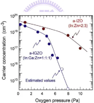
Fig. 1-5 The amorphous formation region (right) and the electron mobilities and concentrations evaluated from the Hall effects for the amorphous thin films (left) in the In2O3- Ga2O3-ZnO system. The thin films were deposited on a glass substrate by PLD under deposition atmosphere of PO2 = 1 Pa. Number in the parenthesis denotes carrier electron concentration.1...8
Fig. 1-6 The carrier concentration as a function of O2 pressure during the deposition in a- InGaZnO4 and a-In2Zn3O6.1...9
Fig. 1-7 (a) The display image of LG’s 3.5” AMOLED (b) Samsung’s AMOLED display driven by InGaZnO TFT...11
Fig. 1-8 The display image of Samsung’s 12.1” WXGA AMOLED display6,7..13
Fig. 2-1 A bottom-gate-top-contact TFT structure...17
Fig. 2-2 The semiconductor energy band diagram when (a) unbiased, (b) negative gate voltage bias, (c) positive gate voltage bias...18
Fig. 2-3 A schematic model of atomic force microscope...23
Fig. 2-4 The contact angle formation of liquid on solid surface...24
Fig. 3-2 Schematic RF sputtering system...31 Fig. 3-3 Schematic DC sputtering system...32 Fig. 4-1 The carrier source of (a) Si, (b) Metal oxide...34 Fig. 4-2 Electrical property of IGZO TFT as a function of oxygen and argon flow rate during deposition.6...35
Fig. 4-3 The AFM result of (a) 0 sccm O2 device deposited for 6.5 mins.
(b) 0.6 sccm O2 device deposited for 8 mins...36
Fig. 4-4 The a-IGZO TFT output characteristics for different oxygen flow rates...38 Fig. 4-5 Annealing 0 to 2 hours for devices of O2 flow rate: (a) 0 sccm, (b) 0.6
sccm...39 Fig. 4-6 The output electrical characteristic comparison for a-IGZO TFTs
post-annealed for 2 and 3 hours...41 Fig. 4-7 The dual stack a-IGZO TFT structure...43 Fig. 4-8 ID-VG curve comparison of the buffered-a-IGZO TFTs...44
Fig 4-9 Contact angle image for water drop on the
(a) Al2O3, (b) HfO2, (c) HMDS, and (d) SiO2 surface...45
Fig. 4-10 The electrical characteristics comparison for a-IGZO TFTs with different source/drain electrodes...49 Fig. 4-11 The work functions of some metallic materials...50 Fig. 4-12 The contact resistance comparison for different source/drain
electrodes...51 Fig. 4-13 The schematic diagram showing the role of (a) oxygen as an electron acceptor and (b) water molecules as a electron donor onto a-IGZO surface.14...54 Fig. 4-14 The negative shift of the threshold voltage over time for a-IGZO TFT with (a) Ti, (b) ITO, (c) Au, and (d) Al source/drain electrodes...56 Fig. 5-1 The Canon’s proposed devise structure on SID’ 08...62 Fig. 5-2 The a-IGZO layer with the Si3N4 passivation layer...62
List of Tables
Table 3-1 The electrode fabrication methods...29 Table 4-1 Contact angle of different buffer layer surface...45 Table 4-2 The performance of the a-IGZO TFTs with the interface modification
layer...46
Chapter 1
Introduction
1.1. Amorphous Semiconductors
An important semiconductor feature is the carrier concentration controllability over several orders of magnitude. Amorphous semiconductors are preferred over polycrystalline ones for active layers from the viewpoints of processing temperature and uniformity of device characteristics.
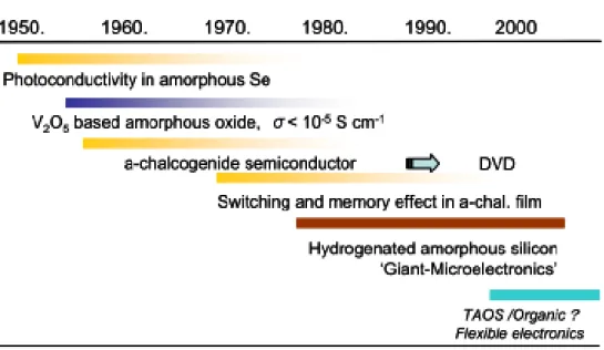
Research on amorphous semiconductors started in 1950s to seek appropriate materials. Fig. 1-1 summarizes the brief history of amorphous semiconductors. The largest impact on electronics is the discovery of hydrogenated amorphous silicon (a-Si:H) by Spear and LeComber in 1975. This is the first material which can control carrier concentration by impurity doping as in crystalline, and it opened a new frontier called ‘Giant Micro- electronics’ which means electronics based on circuits fabricated on a large area substrate. Nowadays, active-matrix flat-panel display (AMFPD) circuits mainly use a-Si:H thin film transistors (TFTs).
Fig. 1-1 History of amorphous semiconductors on new fields.1
Recently, a new electronics is emerging for applications which cannot be fabricated by Si MOS technology. This frontier “flexible electronics” is characterized by electronic circuits fabricated on organic (flexible substrates) instead of inorganic (hard) glasses. The flexible electronic area was born to meet a strong demand for large-area displays because glass substrates are heavy and fragile, and are obviously inconvenient. Amorphous semiconductors are much preferable than crystalline semiconductors for flexible electronics. So far, organic molecule semiconductors have been almost exclusively examined for such applications but their performance and chemical instability are not sufficient for practical applications. Further, the field-effect mobilities of organic TFTs are too low to drive high-resolution,
high speed active matrix organic light emitting diode (AMOLED) displays.1
1.2. Amorphous Oxide Semiconductors
1.2.1. Introduction to Amorphous Oxide Semiconductors
Amorphous oxide semiconductors (AOS) are materials for high performance, low processing temperature electronic devices such as flexible devices due to their high electron mobility >> 10 cm2(Vs)-1 even when their films are deposited at room temperature (RT)
(a) (b)
Fig. 1-2 Flexible transparent TFTs (TIFTs) (a) A photograph of the flexible TIFT sheet bent at R = 30 mm. The TIFT sheet is fully transparent in the visible light range (b) A photograph of the flexible TIFT sheet. The transparent TFT devices are made visible by adjusting the angle of the
illumination2
However, some AOS materials have uncontrollable carriers generated from oxygen vacancy. Therefore, it is important to design and explore a suitable material having both properties of large mobility and stable controllability of carrier concentration for practical applications.
1.2.2. The Carrier Transport Mechanism of AOSs
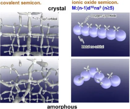
The mobility of a-Si:H (~1 cm2(Vs)-1) is much smaller than that of single crystalline Si (~200 cm2(Vs)-1) due to the intrinsic chemical bonding nature. The average carrier transportation paths in covalent semiconductors, such as a-Si:H, consist of strongly directive sp3 orbitals. The bond angle fluctuation significantly alters the electronic levels, causing high density of deep tail-states, as shown in Fig. 1-3.
In contrast, transparent oxides constituting of heavy post transition metal cations with the (n-1)d10ns0 electron configuration, where n ≥ 5, are the transparent AOS (TAOS) candidates having large mobilities comparable to those of the corresponding crystals. The electron pathway in oxide semiconductor is primarily composed of spatially spread ns orbitals with an isotropic shape, as shown in Fig. 1-3. The direct overlap among the
neighboring ns orbitals is possible. The degree of overlap of the ns orbitals is insensitive to the distorted metal-oxygen-metal bonding. This feature shows why the Hall mobility of AOSs is similar to the corresponding crystalline phase, even under the room temperature deposition of thin-films.
Fig. 1-3 Schematic orbital drawing of electron pathway (conduction band bottom) in conventional silicon-base semiconductor and ionic oxide semiconductor.2
1.3. Amorphous In-Ga-Zn-O TFTs
Transparent AOSs have attracted keen attention since the high performance thin-film transistors can by obtained by using the amorphous In-Ga-Zn-O (a-IGZO) thin films for the semiconductor layers deposited on plastic substrates by pulse-laser deposition (PLD) at room temperature.1 The TFT performance is also confirmed by using the sputter deposition3, which demonstrates the possibility of the large-area applications. The dependence of the TFT characteristics on the metal composition is investigated in detail by a novel combinational approach4, since the multi-metal AOSs can take any ratios of the composition.
1.3.2 The In
2O
3-Ga
2O
3-ZnO Ternary System
For the In2O3-Ga2O3-ZnO ternary system, the incorporation of cations
with large ionic valance such as Ga3+ and Al3+ to high conductive oxides such as In2O3 and ZnO is effective to control the carrier concentration due to
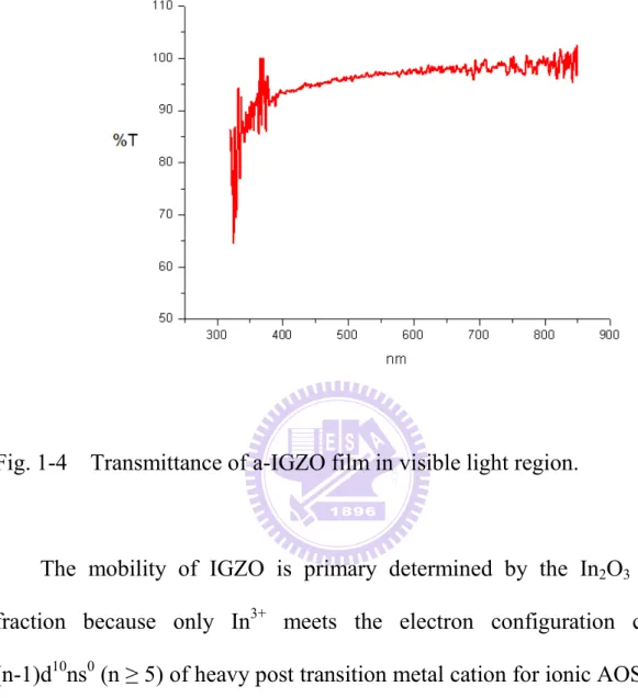
their strong metal-oxygen bonds. Other AOSs, such as a-ITO and c-ZnO have high density carrier density, hence is difficult to control the device characteristics. Besides, amorphous In-Ga-Zn-O (a-IGZO) is transparent throughout the visible spectrum; the transmittance is greater than 80 percent from 400 nm to 850 nm as shown in Fig. 1-4.
Fig. 1-4 Transmittance of a-IGZO film in visible light region.
The mobility of IGZO is primary determined by the In2O3 content
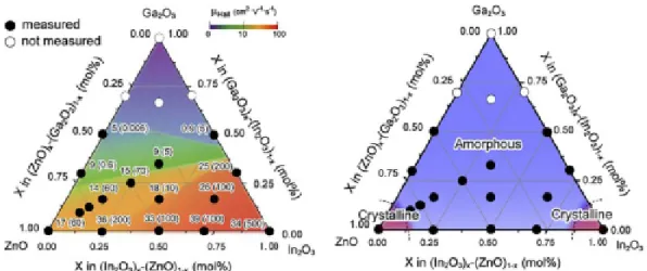
fraction because only In3+ meets the electron configuration criterion (n-1)d10ns0 (n ≥ 5) of heavy post transition metal cation for ionic AOS (IAOS) among the three cations.1 Fig. 1-5 shows the electron mobilities and concentrations evaluated by the Hall effect measurement for amorphous thin films. The mobility is primary determined by the fraction of In2O3 content
and the highest value of ~40cm2(Vs)-1 is obtained for the samples containing the maximum In2O3 fraction.
Fig. 1-5 The amorphous formation region (right) and the electron mobilities and concentrations evaluated from the Hall effects for the amorphous thin films (left) in the In2O3- Ga2O3-ZnO system. The thin films were deposited
on a glass substrate by PLD under deposition atmosphere of PO2 = 1 Pa.
Number in the parenthesis denotes carrier electron concentration.1
The large ionic valence ions such as Ga3+ and Al3+ combine with high conductive oxides such as In2O3 and ZnO to control the carrier concentration
effectively because of the strong metal-oxygen bonds. In other words, Ga3+ suppresses carrier generation via oxygen vacancy formation because Ga ion forms stronger bond with oxygen than Zn and In ions. Therefore, the InGaZnO4 composition was chosen as the AOS for channel layer of the
transparent TFT.
controllability of carrier concentration. This is particularly important for AOSs because electron carriers can be easily generated. It is vital to choose materials which control carrier concentration at low levels (~1014 cm-3) to achieve low off current (Ioff) and large on-off current ratio (Ion/off). In
practice, the effect of binary amorphous materials in the In2O3-ZnO system is
employed in commercial flexible transparent conductive films by depositing on plastic sheet. Thus, the effect of partial oxygen pressure was studied on the carrier concentration in a-InGaZnO4 and a-In2Zn3O6 and the results are
shown in Fig. 1-6.
Fig. 1-6 The carrier concentration as a function of O2 pressure during the
deposition in a- InGaZnO4 and a-In2Zn3O6. 1
below 1013 cm-3 by increasing PO2 to 8 Pa, on the other hand, it remains at
1018 cm-3 in the a-In2Zn3O6 deposited under the same condition. It is
evident that incorporation of Ga3+ is supposed to attract the oxygen ions tightly due to its high ionic potential (+3 valence and small ionic radius), and thereby suppressing electron injection which is caused by oxygen ion escaping from the thin film. The Hall mobility in the samples around the chemical composition of InGaZnO4 is not sensitive to the variation in the
composition, as shown in Fig. 1-6. Thus, the InGaZnO4 system has better
electrical properties than the In2Zn3O6 system.
1.3.3. The a-IGZO TFT State of the Art
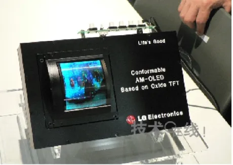
The a-IGZO TFTs process route is the same as a-Si, hence the existing production lines can be used. In 2007, LG Electronics demonstrated a 3.5” AMOLED based on oxide TFT as shown in Fig 1-7 (a). In the same year, Samsung demonstrated a 4” QVGA AMOLED driven by IGZO TFTs, as shown in Fig. 1-7 (b), the mobility of IGZO TFT is 2.6 cm2(Vs)-1.6
(a)
(b)
Fig. 1-7 (a) The display image of LG’s 3.5” AMOLED (b) Samsung’s AMOLED display driven by InGaZnO TFT
TFTs as an active-matrix backplane was demonstrated by Samsung, as shown in Fig. 1-8.
(a)
(c)
Fig. 1-8 The display image of Samsung’s 12.1” WXGA AMOLED display6,7 The a-IGZO TFT exhibited the field-effect mobility (µ) of 8.2 cm2/Vs, threshold voltage (Vth) of 1.1 V, on /off current ratio of > 10
8
, and SS of 0.58 V/decade. Besides, the demonstrated AMOLED display was free from the non-uniformity of pixel luminance, which was attributed to the amorphous nature of a-IGZO semiconductor. The AMOLED display with a-IGZO TFT array is promising for large size applications such as HDTV because a-IGZO thin film can be deposited on the large glass substrate (> Gen. 7) by using conventional sputtering system.
1.4. Motivations
In my thesis research, a-IGZO TFTs are studied for large scale, high speed TFT backplane. For a-IGZO TFTs, the researches rarely focused on the a-IGZO and gate insulator interface properties and effects of source and drain electrodes. We first study the intrinsic properties of a-IGZO TFTs deposited under different oxygen partial pressure; the effects of post-annealing are also discussed. Second, a dual stack TFT structure is introduced for modifying the a-IGZO and gate dielectric interface properties. Furthermore, the effects of different source and drain electrodes are investigated. This study can be a good reference for the transparent electronic applications.
1.5. Thesis Organization
This thesis is divided into five chapters. In Chapter 2, the operation principle of the TFTs is introduced. The measurement and extraction of electrical parameters are also describes. The experiments and equipments for a-IGZO TFTs is described in Chapter 3. In Chapter 4, the electrical properties of a-IGZO films are presented. First, the effects of inlet gas flow ratio and annealing conditions are discussed. Second, the a-IGZO interface conditions and the effects of different source and drain materials on the electrical properties of a-IGZO TFTs are also presented. Finally, conclusions and future works are summarized in Chapter 5.
Chapter 2
Principles and Characterizations of TFTs
______________________________________
In this chapter, the principle of TFTs is first introduced. Second, the measurement and the electrical parameter extraction; including threshold voltage, subthreshold swing, filed-effect mobility and on/off current ratio are presented. Finally, the surface morphology measurement using the atomic force microscope (AFM) and the contact angle measurement are described.
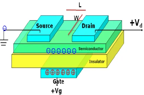
2.1 Operation Principle of TFTs
Conventional TFTs compose of a semiconductor layer, a gate insulator layer, and three electrode terminals including gate, source and drain. The bottom-gate-top-contact TFT structure is shown in Fig. 2-1.
Fig. 2-1 A bottom-gate-top-contact TFT structure.
Transistors can be classified into the depletion-mode and the enhancement-mode, based on whether drain current flows through TFT when no voltage is applied to gate electrode. For the depletion-mode TFT, when the device is on, drain current flows through the device when no gate voltage is applied. For the enhancement-mode TFT, when the device is off, only leakage current flows through the TFT without applying the gate voltage.
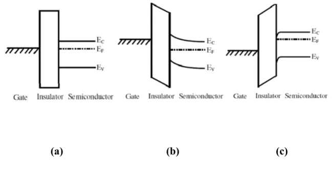
The energy band diagrams through the gate of an n-type enhancement-mode TFT is introduced to explain the three modes of TFT operation, as shown in Fig. 2-2.
(a) (b) (c)
Fig. 2-2 The semiconductor energy band diagram when (a) unbiased, (b) negative gate voltage bias, (c) positive gate voltage bias.
When no gate voltage is applied, the semiconductor is in an equilibrium state. When a negative gate bias is applied, delocalized electrons in the channel are repelled from the semiconductor/gate interface and create a depletion region of positive charge, as indicated by the positive curvature in the conduction band and valance band near the insulator shown in Fig. 2-2 (b). When a positive gate bias is applied, delocalized electrons in the channel are attracted to the semiconductor/insulator interface, creating electron accumulation at the interface, as indicated by the negative curvature in the conduction band and valance band near the insulator in Fig. 2-2 (c). These accumulated electrons at the semiconductor/insulator interface provide a current conduction path and form the channel.
2.2. Electrical Measurement
The device electrical properties were measured by a Keithley 4200 IV analyzer in a light-isolated probe station at room temperature. In IDS-VGS
measurement, the typical drain-to-source bias was swept from VGS = -10 V to
VGS = 30 V. In IDS-VDS measurement, the typical drain-to-source bias was
swept from VDS = 0 V to VDS = 40 V.
2.3. Parameter Extraction Method
In this session, we describe the methods of typical parameters extraction such as threshold voltage (Vth), subthreshold swing (SS), On/Off current ratio
(Ion/Ioff) and field effect mobility (µFE) from device characteristics.
2.3.1. Determination of the V
thThreshold voltage (Vth) was defined from the gate to source voltage at
which carrier conduction happens in TFT channel. Vth is related to the gate
insulator thickness and the flat band voltage.
important parameters of semiconductor devices. This thesis adopts the constant drain current method, that is, the voltage at a specific drain current NID
is taken as Vth, that is, Vth = VG (NID) where Vth is threshold voltage and NID
stands for normalized drain current. Constant current method is adopted in most studies of TFTs. It provides a Vth close to that obtained by the complex
linear extrapolation method. Generally, the threshold current NID = ID/(W/L) is
specified at 1 nA in linear region and at 10 nA in saturation region; W and L represent for TFT channel length and width, respectively.
2.3.2. Determination of the Subthreshold Swing
Subthreshold swing (SS, V / dec.) is a typical parameter to describe the control ability of gate toward channel which is the speed of turning the device on and off. It is defined as the amount of gate voltage required to increase and decrease drain current by one order of magnitude. SS is related to the process, and is irrelevant to device dimensions. SS can be lessened by substrate bias since it is affected by the total trap density including interfacial trap density and bulk density. In this study, SS was defined as one-half of the gate voltage required to decrease the threshold current by two orders of magnitude (from 10-8A to 10-10A). The threshold current was specified to be the drain current when the gate voltage is equal to Vth.
2.3.3. Determination of the Field-Effect Mobility
Typically, the field-effect mobility (µFE) is determined from the
transconductance (gm) at low drain bias (VD = 0.1 V). The TFT transfer I-V
characteristics can be expressed as
] 2 1 ) [( C µ = ID FE ox VG Vth VD VD2 L W − − (2-1) Where
COX is the gate oxide capacitance per unit area,
W is channel width, L is channel length,
Vth is the threshold voltage.
If VD is much smaller than VG – VTH (i.e. VD << VG – Vth) and VG > Vth,
the drain current can be approximated as:
D th G V V V L W ) ( C µ = ID FE ox − (2-2)
The transconductance is defined as:
D V L W ox FE m =µ C g (2-3) Thus, m D OX g WV C L µFE = (2-4)
2.3.4. Determination of On/Off Current Ratio
Drain on/off current ratio is another important factor of TFTs. High on/off current ratio represents not only the large turn-on current but also the small off current (leakage current). It affects AMLCD gray levels (the bright to dark state number) directly.
There are many methods to determine the on and off currents. The practical one is to define the maximum leakage current as off current when drain voltage is applied at 4.5 V.
2.4. Surface Morphology Measurement
The Digital Instruments Dimension 300 atomic force microscope (AFM) was used to characterize the surface morphology of the a-IGZO thin films.
Fig. 2-3 A schematic model of AFM.
The tapping-mode scanning prevents the probe from damaging the sample surface and can get more precise surface topographic information. In the tapping-mode, the probe oscillates up and down regularly. The cantilever vibrates at various frequencies depending on the magnitude of the van der Waals force between the cantilever tip and the sample surface. A laser beam reflected by the cantilever detects the tiny vibration of the cantilever, as shown in Fig. 2-3. The feedback amplitude and the phase signals of the cantilever were recorded by the computer. The amplitude signals provide the morphology information and
the phase signals reveal the material information.
2.5. Contact Angle Measurement
The contact angle is defined by the edge of a liquid droplet on the surface of flat sample; it is formed between the liquid/solid interface and the liquid/vapor interface as illustrated in Fig. 2-4. The static measurement mode is illustrated with a small liquid droplet laying on a flat horizontal solid surface. The static measurement mode is used to estimate wetting properties of a localized region on a solid phase.
Fig. 2-4 The contact angle formation of liquid on solid surface
The contact angle is specific for any given system and is determined by the interactions across the gas-solid-liquid interfaces. The indices s and l stand for
solid and liquid respectively. The symbols σs and σl denote the surface tension
components of the two phases; the symbol γsl represents the interfacial tension
between the two phases, and θ stands for the contact angle corresponding to the angle between vectors σl and γsl. The relationship between these parameters is
Chapter 3
Experimental Methods
_________________________________________
The experimental methods of the fabrication of the a-IGZO TFT are described. Besides, the principle of sputtering system including the RF sputtering and the DC sputtering, is described,
3.1. a-IGZO TFT Device Fabrication
(1) Substrate Cleaning
The detail sequence to clean the n+ heavily doped silicon (Si) is: Step 1: Clean Si wafer by DI water for 3 mins
Step 2: Clean Si wafer by DHF solution for 10 seconds
Step 3: Use N2 purge to dry the Si wafer; place them into a glass container
with a cover.
Step 4: Put the glass container into an oven at 100°C for 1 min
A 300 nm thick silicon oxide (SiO2) for the gate dielectric was thermally
grown in the horizontal furnace by using the low pressure chemical vapor deposition (LPCVD) method. A high quality insulator is required in order to suppress the gate leakage current.
(3) Device Processing Steps
Fig. 3-1 The flow chart of typical a-IGZO TFT device fabrication
Fig. 3-1 shows the preparation of the bottom gate a-IGZO TFT structure used in this study. A heavy doped (N+) prime Si wafer with 300 nm thermal oxide layer was selected as the gate electrode and insulator, respectively. Following, the 40 nm thick source and drain electrodes were deposited through stencil mask openings. The deposition methods for different source and drain are shown in Table 3-1. Finally, a 50 nm thick a-IGZO (In:Ga:Zn = 1:1:1) thin-film was deposited by sputter at room temperature. The RF sputtering was
used for reducing the charges accumulated on the a-IGZO target. The deposition was done with a continuously gas flow of argon and oxygen without intentional substrate heating.
Table 3-1 The electrode fabrication methods.
Finally, the devices were thermally-annealed by a tube furnace in the nitrogen atmosphere at 350°C for defect elimination. In the nitrogen atmosphere at high temperature. Oxygen molecules with only partial bonding on the a-IGZO thin film surface will outgas, and the semiconductor characteristics can be improved.
The channel width (W) of the device were of 600 µm and the channel lengths (L) are 200, 400, 600, 800 or 1000 µm.
Electrical measurement of the a-IGZO TFT was carried out with a probe station system located in a light tight box. The electrical properties of TFTs were measured by a PC controlled Keithley 4200 semiconductor parameter analyzer. For measuring the TFT transfer characteristics, the drain-to-source voltage (VDS) was changed in between 1 and 11 V. The gate-to-source voltage
(VGS) was varied from -10 V to 30 V. All measurements were done at room
temperature in ambient air.
3.2. Sputtering
3.2.1. RF Sputtering
RF sputtering can be applied to the deposition of both insulating and conducting materials. Figure 3-2 shows a RF sputtering system, the substrate is located above the target so that the sputtered atoms can be deposited on to the substrate. A RF power supply generates plasma at the frequency of 13.56 MHz. The plasma creates ions which are accelerated towards the target by a negative DC bias on the target. The ions bombard the target surface and dislodge the target atoms, which then deposit onto the substrate. The sputtering is performed in vacuum, typically between 1 mTorr and 50 mTorr. A lower chamber pressure increases the mean free path, which is the distance between collisions, so that the sputtered target atoms can reach the substrate without scattering away.
Fig. 3-2 Schematic RF sputtering system.
3.2.1. DC Sputtering
DC sputtering has the advantage of higher deposition rate and is less expensive than RF sputtering. A DC sputtering system is shown in Fig. 3-3, the substrate is located above the target and acts as the anode. DC sputtering is commonly applied to deposit conductive materials.
Chapter 4
Results and Discussion
______________________________________
4.1. The Effects of Oxygen Flow Rate and
Post-Annealing on a-IGZO TFTs
4.1.1. Introduction
The carrier source of Si and metal oxide is shown in Fig. 4-1. For Si, the carriers are resulted from impurity doping as shown in Fig. 4-1 (a). Electrons dominate the carrier transport for phosphorous-doped Si. Carrier transport is dominated by holes for boron-doped Si. For metal oxide, the carrier concentration is related to the oxygen vacancy; one oxygen vacancy provides two electrons, as shown in Fig. 4-1 (b).
(a) (b)
Fig. 4-1 The carrier source of (a) Si, (b) Metal oxide.
Because of the oxygen vacancies in the a-IGZO film, a-IGZO TFT characteristics are strongly associated with the a-IGZO film. The reactions on film surface dominate the threshold voltage (Vth) shift. The oxygen absorption
changes the carrier concentration. The oxygen absorption forms depletion layer, resulting in Vth shift.
The oxygen absorption accompanies partial charge transfer, Vth varies at
different oxygen flow rate implies the change in carrier concentration during the absorption and desorption processes. When the oxygen flow rate increases, the channel carrier concentration decreases because of less oxygen vacancies in a-IGZO film. Therefore, higher voltage is needed to turn on the channel. The electrical characteristics of IGZO film can be controlled by varying the deposition conditions (Ar flow rate and O2 flow rate). When the oxygen flow
conductivity is high. When oxygen flow rate is high (over 8 sccm), IGZO film becomes insulator. In intermediate oxygen flow rate (5~8) sccm, IGZO shows semiconductor characteristics and is suitable for channel layer. It is considered that the low oxygen flow rate increases the electrical conductivity of the deposited film.1,5 In the case of Ar gas flow, even though it is not strongly related to electrical property of IGZO film, it is one of the key parameter to control the uniformity of TFT behavior. Fig. 4-2 shows that only in a proper range of PO2 will the a-IGZO exhibit the semiconductor characteristics.
4
In our experiments, several oxygen flow rates (0 sccm, 0.2 sccm, 0.4 sccm, 0.6 sccm, 0.8 sccm) were adopted so as to prepare the a-IGZO TFTs with various electrical characteristics.
Fig. 4-2 Electrical property of IGZO TFT as a function of oxygen and argon flow rate during deposition.6
4.1.2. Results and Discussion
4.1.2.1. Determination of the Deposition Rate
First, the deposition rate of IGZO was determined by measuring the film thickness with the AFM. The AFM results of a-IGZO film thickness are shown in Fig. 3-3. The deposition rate is about 5.933 nm/min for oxygen flow rate = 0 sccm device and 3.537 nm/min for oxygen flow rate = 0.6 sccm device.
(b)
Fig. 4-3 The AFM result of (a) 0 sccm O2 device deposited for 6.5 mins.
(b) 0.6 sccm O2 device deposited for 8 mins
4.1.2.2. The Effects of Oxygen Flow Rate on a-IGZO TFTs
The a-IGZO TFTs were operated in enhancement mode. The SiO2 gate
insulator is 100 nm thick and the post-annealing time is 1.5 hours. Good electrical characteristics like large on-state drain current, small threshold voltage, and low threshold voltage were obtained when the oxygen flow rate is 0 sccm, as shown in Fig.4-4.
-10 0 10 20 30 10-12 10-10 10-8 10-6 10-4
I
DV
G 0 sccm 0.2 sccm 0.4 sccm 0.6 sccm 0.8 sccmFig. 4-4 The a-IGZO TFT output characteristics for different oxygen flow rates.
As a result, under the same post-annealing time, Vth is smaller for smaller
oxygen flow rate. The decrease of Vth is due to the mobile carrier increase.
The mobile carrier increase in channel relates to the oxygen flow rate and affects the channel/dielectric interface by changing the density of interface states. In other words, less oxygen vacancies are filled when the oxygen flow rate is smaller. The oxygen vacancies provide electrons and increase the channel carrier concentration, leading to a smaller Vth.
-20 -10 0 10 20 30 10-13 10-11 10-9 10-7 10-5 I D VG 0 hr 0.5 hr 1 hr 1.5 hr 2 hr (a) -20 -10 0 10 20 30 10-13 10-11 10-9 10-7 10-5
I
DV
G 0 hr 0.5 hr 1 hr 1.5 hr 2 hr (b)4.1.2.3. The Effects of Post-Annealing on a-IGZO TFTs
TFT based on AOSs (e.g. IGO ZTO, ZIO) sputtered in pure Ar requires high annealing temperature (T > 300 ˚C) to exhibit satisfactory electrical characteristics; including better saturation current, smaller hysteresis, and Vth.
The post-annealing effects on device with 300 nm SiO2 gate insulator is
shown in Fig. 4-5. Vth shifts negatively after post-annealing because
post-annealing leads to the lattice structure rearrangement, structural relaxation, and the improved a-IGZO bonding. Post-annealing improves the channel/dielectric interface; and the charge trapping defects are decreased.
The electrical output characteristics for devices post-annealed for 2 and 3 hours are compared in Fig. 4-6. Annealing causes modification of the semiconductor/insulator interface, local atomic rearrangement and improved bonding. Three-hour annealing is the appropriate for a-IGZO TFT with a 300 nm SiO2 gate insulator. Vth shifts negatively to be near 0 V after the thermal
-20 -10 0 10 20 30 40 10-13 10-11 10-9 10-7 10-5
I
DV
G 2 hr 3 hrFig. 4-6 The output electrical characteristic comparison for a-IGZO TFTs post-annealed for 2 and 3 hours.
4-1-3. Conclusions
The oxygen flow rate was varied to examine oxygen absorption effect. The Vth changes with the oxygen flow rate. The oxygen vacancies provide
electrons and increase the channel carrier concentration, leading to a smaller Vth.
Post-annealing improves the crystallinity in a-IGZO because of the semiconductor/insulator interface modification and local atomic rearrangement and the threshold voltage can be adjusted to be near 0 V.
It is found that IGZO thin film transistors are very sensitive to oxygen and can be used as oxygen or pressure sensors.9
4.2. The Interface Modification for a-IGZO TFTs
4.2.1. Introduction
Research for a-IGZO TFT was focused on the intrinsic limitations of semiconductor. A large Vth is still an issue for a-IGZO TFT. It is noteworthy
that a high interface trap density at the semiconductor/dielectric interface increases the Vth. A large Vth leads to the “hard saturation” phenomena in the
electrical output characteristics. Besides, a poor dielectric layer quality leads to the increase of gate leakage current.
In this session, the a-IGZO TFT with the dual-stack structure is introduced, as shown in Fig.4-7. A buffer layer and the gate dielectric insulator were stacked up. The buffer layer is an interface modification layer. The buffer layer materials used in this study were hafnium oxide (HfO2), aluminum oxide
(Al2O3), and hexamethyldisilazane (HMDS). Device with only the SiO2 gate
insulator is for comparison.
Fig. 4-7 The dual stack a-IGZO TFT structure.
The HfO2 and Al2O3 buffer layers are both 10 nm thick, and are deposited
by the e-gun evaporation on SiO2 for the a-IGZO/gate dielectric surface
treatment, as shown in Fig. 4-7. The series capacitance of the SiO2/buffer
layer was dominated by the thicker 300nm SiO2 and the contribution of the
thinner buffer layer was estimated to be of less than 10 %.
4.2.2. Result and Discussion
The buffered-TFT output characteristic comparison is shown in Fig. 4-8. It is noticeable that ID of the HMDS-buffered a-IGZO TFT is increased.
-20 0 20 40 10-13 10-11 10-9 10-7 10-5 I D V G SiO 2 Al2O3 HfO 2 HMDS
Fig. 4-8 ID-VG curve comparison of the buffered-a-IGZO TFTs.
The contact angle measurement result is shown in Fig. 4-9. The water drop on HMDS has the largest contact angle on the HMDS surface, indicating that a-IGZO has improved interfacial condition when it is stacked with a hydrophobic material.
(a) (b)
(c) (d)
Fig 4-9 Contact angle image for water drop on the (a) Al2O3, (b) HfO2, (c) HMDS, and (d) SiO2 surface.
The performance comparison of a-IGZO TFT with the interface modification layer is shown in Table 4-2. The mobility of the HDMS-buffered TFT was enhanced to 13.67 cm2/Vs.
Table 4-2 The performance of the a-IGZO TFTs with the interface modification
layer.
4.2.3. Conclusion
A dual stack TFT structure is introduced to examine the properties of the a-IGZO/gate insulator interface. The interface modification materials adopted in this session are HfO2, Al2O3, and HMDS. As a result, HMDS improves the
field-effect mobility of the a-IGZO TFT. All buffered-TFTs have higher mobility than TFT without the interface modification, indicating that the gate insulator/active layer interface is improved.
From the contact angle measurement; HMDS surface has the largest contact angle for the water drop, indicating that a-IGZO has improved interfacial condition when it is stacked with hydrophobic material HMDS.
The proposed dual layer structure has shown a great potential for the advanced AMLCD technology since the output electrical characteristics of a-IGZO TFTs are greatly related to the conditions of the a-IGZO semiconductor/gate insulator interface.
4.3. The Effects of Source and Drain Electrodes on
a-IGZO TFTs
4.3.1. Introduction
The unmatched source/drain electrodes lead to the high series contact resistance, causing the current suppression phenomena. Furthermore, a high contact resistance induces the current crowding effect and increases the Vth.
Thus, a high efficient contact is necessary to attain electrical properties.
For a-Si:H TFTs, the source to drain resistance is influenced by the contact
of the n+ a-Si:H film, by the interface effect between n+ a-Si:H and source/drain electrodes, and by the intrinsic a-Si:H layer sheet resistance.
Unlike a-Si:H TFTs, the proposed a-IGZO TFT does not have a highly doped ohmic layer, the source to drain resistance is affected by the interface properties between intrinsic a-IGZO and the source/drain metal. These properties are the interface trap, the effective contact area, and the barrier height and width between the a-IGZO semiconductor and the source/drain metal. Compared to a-Si:H TFT, the a-IGZO TFT source to drain resistance is more dependent on the channel resistance, because the interface properties are related to the gate voltage.
In our study, the a-IGZO TFTs were fabricated using materials with different work function for the source/drain electrodes. These materials are as follows: titanium (Ti), gold (Au), aluminum (Al), and indium-tin-oxide (ITO), which is widely used in a-IGZO TFT researches. The chosen electrode materials are widely used not only in the integrated circuit (IC) industry but also in the display applications.
First, the effect of different source and drain electrodes on a-IGZO TFT is investigated. Following, the effect of ambient interactions on a-IGZO TFT without passivation is discussed.
4.3.2. Results and Discussion
4-3-2-1. The Effects of Source/Drain Electrodes on a-IGZO TFTs
The ID-VG characteristics of a-IGZO TFTs with different source/drain
electrodes are shown in Fig. 4-10. The a-IGZO TFT with Ti source/drain electrodes has the highest on-state current (Ion) and the smallest Vth.
-20 -10 0 10 20 30 40 10-13 10-11 10-9 10-7 10-5
I
DV
G Ti ITO Au AlFig. 4-10 The electrical characteristics comparison for a-IGZO TFTs with different source/drain electrodes.
The a-IGZO TFT output characteristics can be related to the work function difference between the a-IGZO semiconductor and the source/drain electrodes. The work functions of several metallic materials are shown in Fig. 4-11. As a
result, Ti has the lowest Vth and Au has the highest Vth.
Figure 4-11 The work functions if some metallic materials.
The work function difference can be related to the contact resistance. The larger the work function difference, the larger the contact resistance. Figure 4-10 shows the contact resistances (Rc) of various source/drains. Generally,
Au has the highest Rc, Al has larger Rc than ITO. Ti provides the lowest Rc,
indicating that Ti provides the smallest work function difference between the source/drain materials and the a-IGZO thin film.
0 20 104 106 108 1010
R
c
(
O
h
m
)
V
G Al Au ITO TiFig. 4-12 The contact resistance comparison for different source/drain electrodes.
The method adopted for extracting Rc is as shown below:
For linear region drain current formula: ID = (W/L)µCox(VG-Vt)VD
Partial differential to drain voltage was taken: ∂ID/∂VD = (Rtotal)-1
Rtotal = Rc + Rch
Rta = Rc + aK ….(1)
Rtb = Rc + bK ….(2)
(2) x a/b ….(3)
From (1) – (3), Rc was obtained.
The comparison for a-IGZO TFT output electrical characteristics with varied source/drain is shown in Table 4-3. A large work function difference between channel and electrodes leads to a large Schottky Barrier and increases Vth. As a result, Au has the largest threshold voltage because Au has the
largest contact resistance for a-IGZO film. In other words, a large contact resistance causes the current crowding effects, leading to a large Vth. On the
other hand, a large contact resistance increases the Schottky Barrier and reduces mobility. In our experiments, for Al, Au, Ti, ITO, the different source/drain electrode materials, the mobilities of a-IGZO TFTs are appropriate for display applications. As a result, the a-IGZO TFT with the Ti source/drain electrodes has high µ, the lowest Vth, and the smallest SS. Therefore, Ti is an appropriate
Table 4-3 Electrical properties comparison for varied electrodes.
4.3.2.2. The Ambient Effects on a-IGZO TFTs
The a-IGZO film is sensitive to the surface absorption of oxygen and water molecules. When the oxygen molecules in atmosphere fill into the oxygen vacancies, they decrease the electrical conductivity of a-IGZO film. In other view, the oxygen vacancies can be assumed as holes and they can assist the electrical conduction of a-IGZO film. Therefore, the filling of oxygen vacancies reduces the electrical conduction of a-IGZO film. On the other hand, there are also oxygen molecules carrying electrons in ambience. They also fill in to the oxygen vacancies, affecting electrical characteristics.
Fig. 4-13 The schematic diagram showing the role of (a) oxygen as an electron acceptor and (b) water molecules as a electron donor onto a-IGZO surface.14
The shift of the Vth over time for a-IGZO TFTs with different source/drain
electrodes is shown in Fig. 4-13. For a-IGZO TFT, the water molecule absorption is the main cause for the shift of threshold voltage. The oxygen molecules are absorbed on both channel and electrodes, but are electrically active only on channel. In atmosphere, the metastable hole traps form in oxide semiconductors. The water molecules diffuse in and out a-IGZO film adversely affects a-IGZO properties.13
-20 0 20 40 10-13 10-11 10-9 10-7 10-5 I D VG 4 hr 3 day 6 day (a) -20 -10 0 10 20 30 40 10-13 10-11 10-9 10-7 10-5 I D V G 4 hr 3 day 6 day (b)
-20 0 20 40 10-13 10-11 10-9 10-7 10-5 I D VG 4 hr 3 day 6 day (c) -20 0 20 40 10-13 10-11 10-9 10-7 10-5 I D VG 4 hr 3 day 6 day (d)
Fig. 4-14 The negative shift of the threshold voltage over time for a-IGZO TFT with (a) Ti, (b) ITO, (c) Au, and (d) Al source/drain electrodes
The absorbed oxygen molecules undergo the partial charge transfer, and form the depletion layer below the a-IGZO active layer surface, hence shifts the threshold voltage positively.
On the other hand, the water molecules on a-IGZO surface act as the electron trapping centers.13 The water molecules absorbed by a-IGZO film form the accumulation layer below the a-IGZO film surface, hence shifts the Vth
negatively. The surface interactions on a-IGZO thin film with the water molecules involves the trap creation/removal in active layer. As a result, the negative Vth shift was observed, indicating that in atmosphere, the interaction
with water molecules is the dominant mechanism for a-IGZO TFT.
4.3.3. Conclusions
The a-IGZO TFTs with varying source/drain materials, which are Ti, Au, Al, and ITO, were fabricated without passivation for investigating electrical performance of the a-IGZO TFT.
First, the output electrical characteristics for a-IGZO TFTs with different source/drain electrodes were compared. The work function difference between a-IGZO active layer and the source/drain electrodes can be considered as the
contact resistance. The larger the work function difference between a-IGZO thin film and the source/drain electrodes leads to the larger contact resistance. The contact resistance is related to the mobility and the threshold voltage. In our experiments, a-IGZO TFT with Au source/drain electrodes has the largest contact resistance. As a result, the higher contact resistance leads to the higher mobility because of the higher carrier injection efficiency. On the other hand, the higher work function difference induces the current crowing effect, leading to the larger threshold voltage. The a-IGZO TFT with Ti source/drain electrodes has the lowest contact resistance; and the device performance is appropriate for the display applications.
Second, since the a-IGZO device without passivation interacts with the atmosphere, the ambience effects were investigated. The oxygen molecules form the electron trapping centers on the a-IGZO surface, thus reduce the carrier concentration. In contrast, the absorbed oxygen molecules deplete electrons while water molecules induce the electron accumulation layer. The water molecule absorption donates the partial electron transfer to the a-IGZO film surface. The water molecule absorption dominates the a-IGZO surface interaction in ambience. As a result, the threshold voltage shifts negatively. Therefore, the adoption of the passivation layer prevents the degradation under humidity. Passivation is the key factor for sustaining the a-IGZO TFT subthreshold properties and the devices reliability.
Chapter 5
Conclusion
______________________________________
5.1. Conclusions
We report on the properties of a-IGZO TFTs fabricated on Si substrate at room temperature using sputtering process.
In the first part, the oxygen flow rate was varied to examine oxygen absorption effect. Vth is smaller for smaller oxygen flow rate, since the
depletion layer underneath the absorption layer forms due to the charge transfer between absorbed O2 and a-IGZO forms.
Post-annealing improves the crystallinity in a-IGZO because of the semiconductor/insulator interface modification and local atomic rearrangement. As a result, the field mobility can be up to 11.42 cm2(Vs)-1 and the threshold voltage can be adjusted to be near 0 V. Our device performance is appropriate for display applications.
examine the properties of the a-IGZO/gate insulator interface. The interface modification materials adopted are HfO2, Al2O3, and HMDS. HMDS greatly
improves the field-effect mobility of the a-IGZO TFT. As a result, HMDS-buffered a-IGZO TFT has larger mobility, implying improved channel/dielectric interfacial condition when it is stacked with the hydrophobic material HMDS.
In the third part, the effects of different source/drain materials on a-IGZO TFT were investigated. The adopted materials are Ti, Au, Al, and ITO.
First, the contact resistance is related to the mobility and the threshold voltage. The higher contact resistance leads to the lower mobility while the higher work function difference leads to the larger threshold voltage. The performance of the a-IGZO TFT with Ti source/drain electrodes is appropriate for the display applications.
Second, since the a-IGZO device without passivation interacts with the atmosphere, the ambience effects were investigated. The oxygen molecules reduce the carrier concentration. In contrast, the water molecule absorption provides electrons. The water molecule absorption dominates the a-IGZO surface interaction in ambience and the threshold voltage shifts negatively.
5.2. Future Work
Recently, the issue of the threshold voltage shift for a-IGZO TFT is a hot topic for fabricating a-IGZO TFT backplane for display application. The Canon’s proposed devise structure on SID’ 08, as shown in Fig. 5-1.
Fig. 5-1 The Canon’s proposed devise structure on SID’ 08.
However, in our future work, the direct Si3N4 passivation on a-IGZO by the
PECVD process will not be adopted since the hydrogen doped Si3N4 will
increase the a-IGZO conductivity, as shown in Fig. 5-2.
In our proposed TFT structure with passivation layer, an oxygen rich SiO2
channel protection layer on the a-IGZO thin film can prevent a-IGZO from losing the O2. A Si3N4 layer can further suppress the active layer surface
interaction with the ambience, as shown in Fig. 5-3.
Fig. 5-3 The proposed structure for a-IGZO passivation.
In addition, the comparison for organic/inorganic passivation will be futher studied and discussed. Ink-jet printing technology will be utilized to process organic materials into TFT devices.
The adoption of the passivation layer prevents the degradation under humidity. Passivation is the key factor for sustaining the subthreshold properties and devices reliability. Based on our previous results, we will further study the effects of organic/inorganic passivation on a-IGZO TFTs. Passivation for a-IGZO TFT opens a potential way to fabricate high performance a-IGZO TFT with good reliability in ambience.
References
_____________________________________________________
[1] H. Hosono, J. Non-Cryst.Sol, 352, 851-858 (2006)
[2] K. Nomura, H. Ohta, A. Takaji, T. Kamlya, M. Hirano, H. Hosono, Nature 432 488 (2004)
[3] K. Nomura, A. Takagi, T. Kamiya, H. Ohta, M. Hirano, and H. Hosono, Jpn.
J. Appl. Phys. 45, 4303-4308 (2006).
[4] H. Yabuta, M. Sato, K. Abe, T. Aiba, T. Den, H. Kumomi, K. Nomura, T. Kamiya and H. Hosono, Appl. Phys. Lett., 89, 112123 (2006)
[5] C. J. Kim, D. H. Kang, I. H. Song, J. C. Park, H. Lim, S. I. Kim, E. H. Lee, R. J. Chung, J. C. Lee, and Y. S. Park, “High stable
Ga2O3-In2O3-ZnO TFT for Active-Matrix Organic Light Emitting
Diode Display Application”, IEDM Tech. Dig., pp. 11.6.1-11.6.4, 2005. [6] J. Y. Kwon, K. S. Son, J. S. Jung, T. S. Kim, M. K. Ryu, K. B. Park, J. W. Kim, Y. G. Lee, C. J. Kim, S. I. Kim, Y. S. Park, S. Y. Lee, and J. M. K, IDW, AMD 9-3, (2007).
[7] P. Barquinha, A. M. Vila, G. Goncalves, L. Pereira, R. Martins, J. R. Morante, and E. Fortuato, IEEE Transactions on Electron Devices, Vol. 55, No. 4, pp. 954-959, (2008)
[8] J. Park, C. Kim, S. Kim, I. Song, S. Kim, D. Kang, H. Lim, H. Yin, R. Jung, E. Lee, J. Lee, K. Kwon, and Y. Park, IEEE Electron Device
Letters, Vol. 29, No. 8, pp. 879-881, (2008).
Lett. 90, 123509 (2007).
[11] K. Seshadri and C. D. Frisbie, Appl. Phys Lett. 78, 993 (2001).
[12] D. Natali, L. Fumagalli, and M. Sampietro, J. Appl. Phys. 101, 12 (2007). [13] P. Barquinha, A. Villa, G. Gonclaves, L. Pereira, R. Martins, J. Morante, and E. Fortunato, phys. Stat. sol (a) 205, No. 8, 1905-1909 (2008)
[14] J. Park, J. Jeong. H. Chung, Y. Mo, and H. Kim, Appl. Phys Lett. 92, 072104 (2008).
[15] H. Hosono, J. Non-Crystalline Solidst. 352, 351-358 (2006).
[16] Y. T. Chou, et al “study on electrical properties of ZrZnO thin film transistor with dual stacks of gate dielectrics”, ICMCTF 2008.
[17] J. Nishi, et al, Jpn. J. Appl. Phys. Vol. 42, p. L347-L349 (2003). [18] P. F. Carcia, R. S. Mclean, and M. H. Reilly, Appl. Phys. Lett. 88, 123509 (2006).
[19] D. Kang, I. Song, C. Kim, Y. Park, Appl. Phys. Lett., 91, 091910 (2007) [20] H. Q. Chiang, B. R. Mcfarlane, D. Hong, R. E. Presley, J. F. Wager, Journal of Non-Crystalline Solids, 354, 2826-2830 (2008)